
The Design of a Fully Differential Capacitive Pressure Sensor
with Unbalanced Parasitic Input Capacitances
in 130nm CMOS Technology
B. T. Bradford, W. Krautschneider and D. Schroeder
Institute of Nanoelectronics, Hamburg University of Technology, Eissendorfer Strasse 38, Hamburg, Germany
Keywords:
Capacitive Pressure Sensor, Correlated Double Sampling, SC Noise Analysis.
Abstract:
A switched capacitor amplifier for measuring absolute pressure with a micro-machined capacitive pressure
sensor using correlated double sampling has been designed in 130nm CMOS technology. The switched
capacitor amplifier design uses a combination of correlated double sampling, input offset cancellation, and
output offset cancellation to help reject
1
f
noise and DC offset mismatch. A method for sizing the opera-
tional transconductance amplifier (OTA) components according to the system noise, accuracy, and bandwidth
requirements is presented.
1 INTRODUCTION
This paper will describe the design of a system for
measuring absolute pressure with a micro-machined
capacitive pressure sensor. The design will be used
in a blood pressure sensing wireless medical implant
(Buhk et al., 2010) which will be permanently im-
planted inside an artery and powered through RF in-
ductive wireless power transmission (Bradford et al.,
2012).
The wireless implant will be placed inside of the
artery whose pressure it should monitor, necessitating
small size and low power consumption. The goal of
the whole design process is to create a system which
delivers the required sensor resolution, at the neces-
sary noise levels, with the lowest power budget.
2 CAPACITIVE PRESSURE
SENSOR
The theory of operation of a capacitive pressure sen-
sor is based upon the general formula for capacitance
C =
εA
d
where ε is the relative permittivity, A is the area, and
d is the separation between the capacitor’s two elec-
trode plates. When pressure is applied to the sen-
sor, the electrode plates are squeezed together result-
ing in a larger capacitance value. The circuit which
is used to stimulate the capacitive pressure sensor is
the capacitive bridge from Figure 1, and everywhere
throughout the system, the switches S0 and S1 are ac-
tivated by non-overlapping clocks.
S1
S0
Vstim
Co+Cs
Co
S1
Va
Co
Vb
S0
Vstim
Co
Figure 1: The capacitive pressure sensor as part of a capac-
i
tive bridge.
The pressure sensing capacitor has a nominal ca-
pacitanceC
0
and a sense capacitanceC
s
which is a lin-
ear function of the applied pressure. Using superposi-
tion theory, the change in voltage at nodeV
a
generated
by the switch transition S
0
→ S
1
can be calculated as
a function of V
stim
(1).
∆V
ab
= V
stim
C
s
C
s
+ 2C
0
(1)
The maximum expected input signal peak-peak
swing ∆V
ab
max
pp
can be calculated by substituting C
s
with the maximum expected peak-peak capacitances
of ±
C
s
max
2
. For the output swing, if V
DD
is the max-
imum output voltage level, V
out
pp
= 2 V
DD
, and the
137
T. Bradford B., Krautschneider W. and Schroeder D..
The Design of a Fully Differential Capacitive Pressure Sensor with Unbalanced Parasitic Input Capacitances in 130nm CMOS Technology.
DOI: 10.5220/0004237801370142
In Proceedings of the International Conference on Biomedical Electronics and Devices (BIODEVICES-2013), pages 137-142
ISBN: 978-989-8565-34-1
Copyright
c
2013 SCITEPRESS (Science and Technology Publications, Lda.)

required closed loop gain (2) can be used to find the
value for the feedback capacitance C
f
in Figure 2.
A
cl
=
2 V
stim
∆V
ab
max
pp
=
2 C
0
C
f
(2)
C
f
=
2C
0
A
cl
(3)
3 SC NOISE ANALYSIS
The SC amplifier is a fully differential SC am-
plifier with input and output offset compensation
(Fig. 2) (Enz and Temes, 1996). During SC switch
phase S0, the amplifier is in unity gain configuration
where the OTA’s DC offset voltage V
os
and the sys-
tem noise voltage V
x
ab
S0
noise
are sampled across the
nodes V
x
ab
(4). During phase S1, V
os
, the system noise
voltageV
x
ab
S1
noise
, and the capacitance to voltage con-
version result, ∆V
ab
, are applied across V
x
ab
(5).
S0
Vstim
Co+Cs
Co
S1
Cbondpad
Vstim
C
gs
S1
S0’
Cf
S0’
S0
Cl
S1
S1
S1
S0
S1
Cf
Co
C
gs
Vxb
Vxa
Co
S0
Vcm
Vcm
Figure 2: Schematic of the capacitive bridge and the SC
amplifier with associated parasitic capacitances.
V
x
ab
S0
= V
os
+V
x
ab
S0
noise
(4)
V
x
ab
S1
= V
os
+V
x
ab
S1
noise
+ ∆V
ab
(5)
V
x
ab
S1−S0
= ∆V
a
+V
x
ab
S0
noise
+V
x
ab
S1
noise
(6)
3.1 SC Noise Analysis for Phase S0
To determine the noise from switch phase S0, the cir-
cuit from Fig. 2 can be reduced to the circuit in Fig-
ure 3.
2Co
Cpar2
S0
2Co
Cpar1
S0
S0’
Cf
1/gm
Vxb
S0
S0
S0’
R =2/gmeff
S0’
Cf
2Co Cgs
Cbondpad
Cf
2Co Cgs
S0’
4kT /gmγnf
1/gm
Vxa
Vxb
Vxa
2*4kT /gmγnf
4kT /gmγnf
Figure 3: Schematic of the SC amplifier during phase S0.
The circuit from Figure 3 has the OTA in unity
gain feedback which results in a differential thermal
output noise voltage which is equal to the sum of the
OTA’s input devices’ input referred noise voltages (7).
V
2
noise
OTA
= 2∗
4kT
γ
in
gm
nf (7)
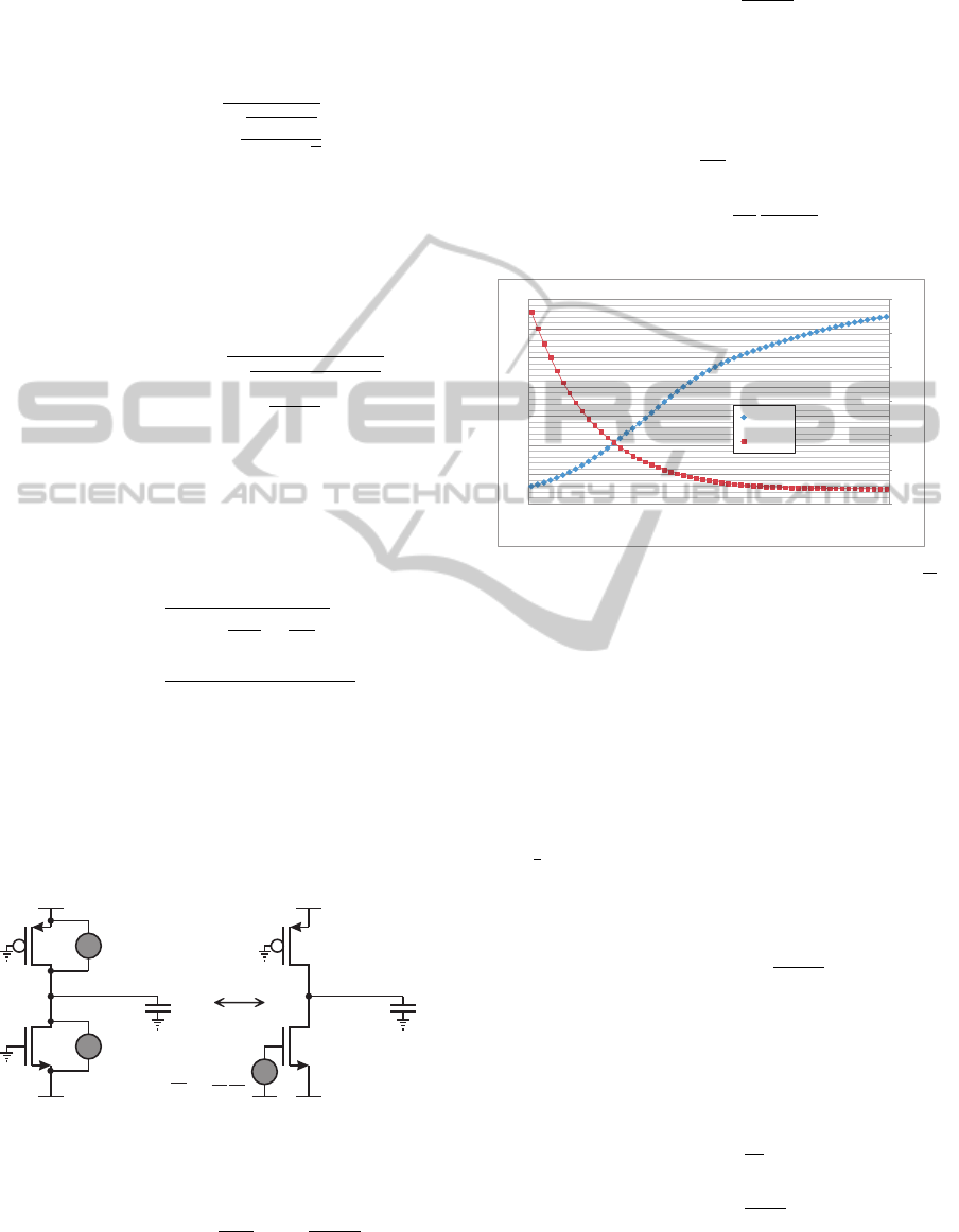
The γ factor for this 130 nm CMOS technology has
been determined by performing Spectre small signal
noise analysis simulations (Figure 4). The simulation
results show that the γ factor has a strong correlation
to the MOSFET’s transconductance efficiency η
gm
=
gm
I
d
.
10
20
25
30
35
20μ
0.25
0.3
0.35
0.4
0.45
0.5
0.55
0.6
0.65
0.7
0.75
ChannelLength L
Transcondu
ctance Efficiency
γ -gammafactor
0.3
0.35
0.4
0.45
0.5
0.55
0.6
0.65
0.7
15
200n
2μ
Figure 4: Plot of the γ noise factor against the channel
length and transconductance efficiency. The data was col-
lected by performing SPICE small signal noise simulations
on a 130 nm CMOS technology NMOS device.
From (7), nf is the noise factor which scales
the OTA’s input MOSFET device’s input referred
noise up to the total output noise voltage of the
OTA (Sec. 4.1). The OTA’s thermal output noise is
bandwidth limited by the noise equivalent bandwidth
(NEB) (9) (Baker, 2011).
NEB = GBW
π
2
GBW =
gm
2π(2 C
eq
)
(8)
NEB =
gm
4(2C
eq
)
(9)
The parameter C
eq
is the differential load capaci-
tance across the outputs of the OTA during switching
phase S0. At the nominal pressure where C
s
= 0, C
eq
can be derived as (10).
C
eq
a
= 2C
0
+C
par1
+C
f
C
eq
b
= 2C
0
+C
par2
+C
f
C
eq
=
C
eq
a
C
eq
b
C
eq
a
+C
eq
b
(10)
The OTA input referred thermal noise, (7), multi-
plied by the NEB (9) which is bandwidth-limited by
C
eq
(10) results in a noise voltage across V
x
ab
of (11)
BIODEVICES2013-InternationalConferenceonBiomedicalElectronicsandDevices
138

V
2
x
ab
S0
noise
=
kT
C
eq
γ
in
nf (11)
After the SC amplifier has switched to phase S1,
the noise charge gets transferred to the output nodes
as a function of the feedback factor F (12).
V
out
=
V
x
ab
F
(12)
2Co
C
par2
S1
2Co
C
par1
Cf
S1
S1
V
xb
Vxa
S1
Cf
V
xb
Cf
2Co
Cf
2Co
C
par1
V
xa
Cpar2
_
+
Vout
_
+
Vout
Figure 5: Equivalent schematic for determining the feed-
back factor (13).
From Figure 5, F is the transfer function from the
OTA’s output to its input (13).
F =
V
x
ab
V
out
=
C
f
2
C
f
2
+
(2C
0
+C
par1
)(2C
0
+C
par2
)
(2C
0
+C
par1
)+(2C
0
+C
par2
)
(13)
The final output noise contribution from phase S0
is found by combining (11), (12), and (13) into (14).
V
2
out
noise
S0
=
kT
C
eq
γ
in
nf
F
2
(14)
3.2 SC Noise Analysis for Phase S1
The switches in the feedback and output path of
the circuit can be ignored if their resistance R
sw
≪
1
gm F
(Murmann, 2012). The two remaining S1 noise
sources are the input switch resistive noise and the
OTA input referred noise voltage (Figure 6).
2Co
C
par2
S1
2Co
C
par1
Cf
S1
Cl
Vx
b
Vxa
S1
Cf
2*4kT /gmγ
4kTR
S1
S1
S1
S1
*nf
4kTRS1
Figure 6: Schematic of the SC amplifier during phase S1.
First, considering the switch input noise, the S1
switch noise generators produce a differential noise
voltage V
2
noise
input
= 2 ∗4kTR
S1
. This noise voltage is
amplified by the closed loop gain of the amplifier, A
cl
,
and it is energy limited by the NEB resulting in a total
input switch noise contribution of (15).
V
2
out
noise
R
S1
= (2∗4kTR
S1
) A
2
cl
NEB
V
2
out
noise
R
S1
=
kT
C
leff
A
2
cl
R
S1
gm F (15)
The other noise contributor for phase S1 is the
OTA’s thermal noise. As it was for switching phase
S0, the input referred thermal noise of the OTA is (7),
and the output noise is the input noise divided by F
and bounded by the NEB (16).
V
2
onoise
OTA
= 8kT
γ
in
nf
gm
1
F
2
gm F
8 C
leff
V
2
onoise
OTA
=
kT
C
leff
γ
in
nf
F
(16)
Vxb
Cf
2Co
Cf
2Co
Cpar1
Vx
a
Cpar2
Cl
Figure 7: The circuit used to determine the OTA effective
output capacitance C
leff
.
Figure 7 can be used to calculate C
leff
, and after a
bit of algebra, C
leff
can be expressed as (17).
C
leff
= C
l
+
C
f
2
(1−F) (17)
Summing the two noises (15) and (16) results
in (18), which is the total SC phase S1 noise contribu-
tion.
V
2
noise
S1
=
kT
C
leff
A
2
cl
R
S1
gm F +
γ
in
nf
F
(18)
From (18), if the following condition is fulfilled:
A
2
cl
R
S1
gm F ≪
γ
in
nf
F
then it is safe to consider only the OTA’s noise con-
tribution for the phase S1 noise. With this simplifi-
cation, (14) and (16) can be summed together to give
the total system noise (19).
V
2
noise
total
= kT
γ
in
nf
F
1
C
eq
F
+
1
C
leff
(19)
TheDesignofaFullyDifferentialCapacitivePressureSensorwithUnbalancedParasiticInputCapacitancesin130nm
CMOSTechnology
139
4 NOISE FACTOR AND Cl
For an ADC with an N bit resolution, the total allow-
able error is (20).
ε
2
total
=
V
2
signal
rms
10
6.02∗N+1.76
10
(20)
ε
total
pp
=
q
ε
2
total
2
√
2 (21)
Eq. (21) gives the peak-peak noise error budget
for the system. The required thermal noise SNR is
increased by a few dB, denoted by SNR
extra
in (22),
so that only a fraction of the total error will be given
to noise (23).
ε
2
noise
rms
=
V
2
signal
rms
10
6.02∗N+1.76+SNR
extra
10
(22)
noise fraction = 10
−
SNR
extra
10
(23)
Choosing a value for C
gs
based upon its expected
length and width, then C
eq
and F can be solved.
(19) and (22) can be combined to form (24) and (25),
from which the nf or theC
leff
can be determined based
on the circuit noise requirements.
nf =
ε
2
noise
F
kTγ
in
1
C
eq
F
+
1
C
leff
(24)
C
leff
=
kTγ
in
nf C
eq
F
ε
2
noise
F
2
C
eq
−kTγ
in
nf
(25)
4.1 Noise Factor Determination
The total OTA noise is a summation of the 4kTγ gm
noise currents to the output (26), and the OTA noise
factor, nf, input refers the total output noise to the in-
put device gm by dividing by gm
2
1
(27).
M2
M1
M2
M1
Cl Cl
²
V
ninput=4kT
γ1
gm1
1+
gm2
gm1
γ2
γ1
)(
InM1=4kT gmγ1 1
²
I
nM2=4kT gmγ2 2
²
I =gm V
noise n1 input
²² ²
I =I +Inoise n nM1 M2
²
²²
Figure 8: Input referred system noise current.
I
2
noise
out
= 4kT (γ
1
gm
1
+ γ
2
gm
2
) (26)
V
2
noise
input
= 4kT
γ
1
gm
1
1+
γ
2
gm
2
γ
1
gm
1
(27)
nf =
1+
γ
2
gm
2
γ
1
gm
1
(28)
The nf design parameter can be expressed in terms
of transconductance efficiency values (29), normal-
ized to the input device drain current (30).
η
gm
=
gm
I
d
(29)
nf = 1+
I
d
2
I
d
1
γ
2
η
gm
2
γ
1
η
gm
1
(30)
0
100
200
300
400
500
600
0
5
10
15
20
25
30
35
0.02
0.02
0.03
0.04
0.06
0.09
0.13
0.18
0.25
0.35
0.50
0.71
1.00
1.41
2.00
2.83
4.00
5.66
8.00
11.31
16.00
22.63
32.00
45.26
64.00
90.51
128.00
181.02
256.00
MOSFET SaturationVoltageVdsatmV
gmoverIdTransconductnceEfficiency
W/L ratio forId=1µA
NType
gmoverid
Vdsat
Figure 9: Spectre simulation results sweeping channel
W
L
ratio with fixed I
d
= 1µA of a 130nm N-type MOSFET.
Using the data from Figures 4 and 9, γ and η
gm
values can be chosen which allows the amplifier to
meet the nf and output swing requirements.
4.2 Gain, Settling and gm
The remaining error available for the settling is (31),
and the gain and bandwidth of the amplifier must be
great enough to settle the output to within ε
settle
in
only
1
2
period of the SC amplifier clock. The settling
error is comprised of the static error, ε
static
(33), and
the dynamic error, ε
dynamic
(34).
ε
settling
= ε
total
pp
1−10
−
SNR
extra
10
(31)
The amplifier’s loop transfer function T
0
(32) de-
termines the static error (33) of the analog conversion,
where A
0
is the open loop gain of the amplifier.
T
0
= A
0
F (32)
ε
static
=
1
T
0
ε
static
=
1
A
0
F
(33)
The dynamic error of the amplifier is determined
using the amount of time available to settle, t
s
, and the
BIODEVICES2013-InternationalConferenceonBiomedicalElectronicsandDevices
140

τ = R
OTA
C
load
time constant of the OTA (34). At low
SC clock speeds, t
s
is
1
2
the SC system clock period,
R
OTA
is the effective resistance.
1
gm F
, of the amplifier,
and C
load
= 2 C
leff
is the effective output capacitance
of the OTA output node.
ε
dynamic
= e
−
t
s
τ
ε
dynamic
= e
−
gm F
4 f
sc
C
leff
(34)
Equations (33) and (34) can be combined to
form (35).
ε
settle
= ε
static
+ ε
dynamic
gm = −
4C
leff
f
sc
F
ln
ε
settling
−ε
static
(35)
For gm to be real and finite (36) must be true.
A
0
>
1
ε
settling
F
(36)
Solving (35) for minimum open loop gain results in
infinite gm, and solving for minimum gm requires in-
finite A
0
(Fig. 11). Increasing A
0
by a few dB quickly
results in near minimum gm requirements. With gm
from (35), and the input transistor η
gm
ratio for the
required nf, then the drain current through each input
device is (37).
I
d
=
gm
η
gm
(37)
With I
d
and η
gm
, Figure 9 can be used size the
W
L
ratio
for each transistor.
5 SC AMPLIFIER DESIGN
EXAMPLES
The system has been designed to measure absolute
pressure with the Protron-Mikrotechnik capacitive
absolute pressure sensor using a 1.2 VDC stimulation
voltage at the human body temperature of 38
◦
C. Ta-
ble 1 lists the design parameters which are to be used
in the SC amplifier design.
Three different designs have been created with the
Cadence Design Framework using the UMC 130nm
technology, and the design variables are listed in Ta-
ble 2. The amplifier architecture which is used for
each design is the gain boosted folded cascode am-
plifier from Figure 10 (Bradford et al., 2013) which
is able to provide 102 dB of gain over the required
±850 mV of output swing. Eq. (38) is used to select
the γ and η
g
m values for the amplifier.
nf = 1+
I
d
2
I
d
1
γ
2
η
gm
2
γ
1
η
gm
1
+
I
d
5
I
d
1
γ
5
η
gm
5
γ
1
η
gm
1
(38)
Plotting (35) for f
sc
= 4kHz, Figure 11, allows a
system gm to be selected based on an open loop gain
of A
0
= 102 dB.
Table 1: Pressure sensor system design constants.
Temperature 38
◦
C
2 C
0
12.0 pF
C
swing
pp
1.6 pF
V
ab
max
pp
(1) 160 mV
V
out
pp
2.4 V
A
cl
(2) 15
V
V
C
f
(3) 800 fF
C
bondpad
5.5 pF
C
l
4.6 pF
V
stim
1.2 VDC
ε
total
(20) 1.172 mV
Table 2: CDS system design values.
f
sc
4ksps 40ksps 400ksps
C
gs
100fF 500fF 1.5pF
C
eq
(10) 7.58pF 7.79pF 8.3pF
F (13) 0.053
V
V
0.051
V
V
0.048
V
V
C
leff
(17) 4.98pF 4.98pF 4.99pF
SNR
extra
(22) 2.2 dB 2.1dB 2.1dB
ε
noise
rms
(22) 522 µV 529µV 529 µV
ε
settling
(31) 452 µV 436µV 420u µV
nf
max
(24) 3.62 3.60 2.69
gm
min
(35) 11.6 µS 120 µS 1.282 mS
A
0
min
(36) 92.4dB 93.0dB 98.9dB
η
gm
in
Fig. 9 28 28 25
γ
in
Fig. 4 0.35 0.35 0.45
η
gm
load
Fig. 9 14 14 14
γ
load
Fig. 4 0.6 0.6 0.6
nf (38) 3.57 3.57 2.6
A
0
Fig. 11 102dB 102dB 102dB
gm Fig. 11 12.3µS 126 µS 1.364mS
I
d
(37) 440 nA 4.29 µA 54.6 µA
OUT+ OUT-
GB_P
M4A
M5BM5A
IN+
IN-
M1BM1A
M4B
GB_N
Vcmfb
Vb1
Vb4
Vocm=Vb3
Vocm=Vb4
Vb6
M3CM3B
M2C
M2A M2B
M3A
Figure 10: The gain boosted folded cascode amplifier.
5.1 Amplifier Design Verification
DC simulations are used to fine tune the transistor
dimensions until they have the desired η
gm
values.
TheDesignofaFullyDifferentialCapacitivePressureSensorwithUnbalancedParasiticInputCapacitancesin130nm
CMOSTechnology
141

90 100 110 120 130 140
12
13
14
15
16
17
18
19
20
OpenLoopGaindB
Transconductance Sμ
A mino
gmmin
Figure 11: Plot of gm versus A
0
from (35) for f
sc
= 4kHz
showing asymptotic behavior at minimum gm and mini-
mum A
0
.
Then, two different analyses, ac and pss/pnoise, are
performed on each of the three amplifiers. The ac
analysis is used to find the amplifier’s GBW, and the
pss/noise is used to verify the V
2
noise
rms
of the circuit.
The three amplifiers are simulated using the exact de-
vice η
gm
and I
d
values listed in Table 2 without any
further optimizations, and the pss/noise simulation is
performed as per the guidelines documented in (Mur-
mann, 2012).
Table 3: Spectre noise analysis simulation results.
f
sc
4 kHz 40 kHz 400 kHz
GBW (8) 196 kHz 2.013MHz 21.79 MHz
GBW
simulation
206.5 kHz 2.086 MHz 22.32 MHz
ε
noise
rms
(22) 522 µV
rms
529 µV
rms
529 µV
rms
V
2
noise
rms
simulation
487 µV
rms
507 µV
rms
547 µV
rms
6 CONCLUSIONS
This paper has presented a method for measuring
a commercially available micro-machined capacitive
pressure sensor with a switched capacitor amplifier
using correlated double sampling. The SC ampli-
fier, with its unbalanced input load capacitances, is
analyzed for noise and bandwidth requirements. A
method for designing the amplifier to meet the noise
requirements as a function of the OTA noise factor
nf and transconductance efficiency values, η
gm
, has
been presented. In addition to the noise requirements,
a method for achieving the settling requirements as
a function of the SC frequency and the system open
loop gain has been presented. This method for am-
plifier design was implemented using the Cadence
Design Framework II, and verified using various Ca-
dence Virtuoso Spectre simulations over an operating
frequency range spanning three decades from 4 kHz
to 400 kHz.
REFERENCES
Baker, R. (2011). CMOS: Circuit Design, Layout, and Sim-
ulation. IEEE Press Series on Microelectronic Sys-
tems. Wiley.
Bradford, B., Krautschneider, W., and Schroeder, D. (2012).
Wireless power transmission for powering medical
implants situated in an abdominal aortic aneurysm.
In 46th annual conference of the German Society for
Biomedical Engineering (BMT 2012), pages 941–944,
Jena, Germany.
Bradford, B., Krautschneider, W., and Schroeder, D. (2013).
A gain boosted folded cascode using telescopic boost-
ing amplifiers with switched capacitor input level
shifters. The IASTED International Conference,
Biomedical Engineering.
Buhk, J., Bradford, B., Koops, A., Schroeder, D.,
Krautschneider, W., and Adam, G. (2010). An in-
tegrated stent-graft for non-invasive 4-dimensional
aneurysm sac pressure monitoring after endovascular
aortic aneurysm repair. In RSNA 2010, pages LL–
VIS–WE4A, Chicago, Il, USA.
Enz, C. C. and Temes, G. C. (1996). Circuit techniques for
reducing the effects of op-amp imperfections: autoze-
roing, correlated double sampling, and chopper stabi-
lization. Proceedings of the IEEE, 84(11):1584–1614.
Murmann, B. (2012). Thermal noise in track-and-hold cir-
cuits: Analysis and simulation techniques. Solid-State
Circuits Magazine, IEEE, 4(2):46 –54.
BIODEVICES2013-InternationalConferenceonBiomedicalElectronicsandDevices
142
