
Analysis of Fault Injection in Implantable Capacitive Blood-pressure
Sensors
J. A. Miguel, Y. Lechuga and M. Martinez
Technology Electronics, Automatic and System Engineering Department, University of Cantabria,
Avda de los Castros s/n, Santander, Spain
Keywords: MEMS Testing, Fault Injection, Fault Modelling, Finite-element Analysis, Capacitive Pressure Sensor.
Abstract: This work explores the fault injection problem in the particular case of an implantable capacitive micro-
electromechanical pressure sensor for blood-flow measurement applied to the detection of in-stent
restenosis. In order to develop a MEMS testing method for this sensor and its related electronic circuitry, an
accurate and realistic fault model is essential. A behavioural description of the equivalent capacitance in the
fault-free case can be obtained from the analytical and numerical solutions of the deflection of a circular
diaphragm under a uniformly distributed pressure. However, the deflection problem for faulty conditions
due to, for example, contamination-based defects or partially released structures must be solved and
modelled using finite-element analysis.
1 INTRODUCTION
Vascular diseases are the leading mortality cause in
the European Union, being responsible of the 40%
of all deaths in the year 2008 (OECD, 2010). The
use of angioplasties and vascular stents has become
the most frequently used method for the treatment of
the most common vascular illness, such as blood
vessels stenosis, aortic aneurysms, arteriosclerosis
and renovascular hypertension.
However, in-stent restenosis (ISR), due to
neointimal tissue growth inside an implanted stent,
keeps on being the major drawback in stent
implantation, seriously compromising its long-term
results. The recent appearance of the so called
intelligent stents involves a potential economical
solution to this problem. An intelligent stent (e-
stent) incorporates a sensor capable of monitoring
and transmitting real-time measurements of
biological parameters related to blood-flow quality.
There are three typical approaches for designing the
aforementioned intelligent stents, regarding the
nature of the biological parameters and the way they
are measured: capacitive pressure measurements,
electromagnetic blood flow measurements and
ultrasonic blood flow measurements.
It is important to point out that an implantable
sensor for any of these techniques must match
certain characteristics, including reduced size, output
stability, low power consumption, low cost and
above all, reliability over extended time period. This
fact makes testing and thus, realistic fault injection
and fault modeling, a critical issue.
The objective of this work focuses on fault
model generation for an implantable capacitive
MEMS pressure sensor utilized to measure blood-
flow velocity. This model will allow the future
development of a comprehensive MEMS testing
methodology.
Continued success for MEMS will require cost-
effective methods of manufacturing. Advances in
this area must include a testing methodology that
allows products to be economically tested while
ensuring high quality and reliability. This is
especially important in applications where MEMS
are integral parts of safety-critical systems such as
implantable biomedical devices.
Traditionally, manufacturers focus on partially
checking the functionality of MEMS by performing
certain electrical, optical, mechanical or
environmental measurements (Wang et al., 2008).
However, there is a need to obtain correlations
between failure modes and the underlying physical
causes. These relationships will allow accurate
modeling of complex effects that can be used in fault
model generation, fault diagnosis and in the
development of efficient testing techniques.
153
Miguel J., Lechuga Y. and Martinez M..
Analysis of Fault Injection in Implantable Capacitive Blood-pressure Sensors.
DOI: 10.5220/0004241701530158
In Proceedings of the International Conference on Biomedical Electronics and Devices (BIODEVICES-2013), pages 153-158
ISBN: 978-989-8565-34-1
Copyright
c
2013 SCITEPRESS (Science and Technology Publications, Lda.)

Thus, success of any MEMS testing
methodology is highly dependent on the fault
models employed. Fault models that do not include
real defective behavior can reduce defect coverage,
degrade test quality and, therefore, the reliability of
the implantable sensor.
MEMS fault models must explicitly consider the
impact of defects on the micromechanical structures.
Our approach centers on the inductive generation of
the possible faulty behaviors from realistic finite-
element simulations. Particularly for those faults
whose behavior cannot be easily described by an
analytical model, as in the fault-free case.
Section 2 introduces the most common failure
mechanisms that can affect MEMS devices. In
Section 3 the capacitive pressure sensor chosen as
system under test is presented. Section 4 describes
the need of finite-element (FE) analysis for
modeling faults such as incomplete release of
suspended elements and contamination, in the case
of diaphragm or membrane-based MEMS pressure
sensors. Finally, in Section 5 conclusions are
presented.
2 FAILURE MECHANISMS AND
FAULT CLASSES
Among the failure mechanisms or defects which can
appear during fabrication, defects occurring during
the CMOS process can be distinguished from defects
occurring during micromachining (Castillejo et al.,
1998); (Mir et al., 2000); (Huang et al., 2012).
Microelectronic and micromechanical
components are created on the wafer during the
CMOS process by means of a set of semiconductor,
conductor and dielectric layers. These layers are
obtained through technological operations such us:
oxidation, deposition, photolithography, etching, ion
implantation or annealing. Each one of them is a
potential source of defects. Therefore, as a result of a
technological step, contaminants or residuals may
remain in the environment and be harmful in a
succeeding step.
For example, one of the most common problems
encountered for the fabrication of CMOS-
compatible MEMS is the presence of oxide residuals
in areas of naked silicon exposed for
micromachining. These oxide residuals can be
formed from thermal silica and from different layers
of oxides which have not been properly cleaned, and
can prevent the formation of an adequate cavity
during micromachining of the exposed silicon.
During micromachining, anisotropic etching
outside the foundry is used to suspend the structures.
For surface micromachining, a sacrificial layer of a
material such as silicon oxide, polysilicon, porous
silicon or aluminium is deposited. The
postprocessing operation removes this sacrificial
layer to suspend the microstructure. However, a
suspended microstructure may not be fully released,
or the cavity produced may be inadequate, due to
several mechanisms that include, not only the
presence of unwanted oxide residuals, but also
insufficient etching time, slow etching rate because
of an inadequate solution, re-depositions after
etching, or the formation of complex substances
from etching chemical reactions. These substances
may affect the quality of the solution, reducing
etching rate or appear stuck on the microstructure at
the end of the process.
Failure mechanisms can be classified according
to the physical properties or parameters of the
MEMS which are affected. In summary, each group
of faults (affecting the gauge that provides the actual
electrical interface or the microstructure that
suspends the gauge) is in turn classified in two
classes: catastrophic faults, which prevent any
system utilization, and parametric faults, for which
changes on geometrical or material parameters alter
microsystem performance.
Stiction to the bulk or the inadequate release due
to incomplete etching of a suspended structure can
mostly occur for both surface and bulk
micromachining. With such faults, a seismic mass
may remain stuck, for example, in the case of an
accelerometer, or the geometry and clamping
conditions of the membrane of a capacitive pressure
sensor may be significantly affected. Besides that,
particle contamination may also give rise to
catastrophic or parametric faults, depending on their
position, geometry, and size.
For example, highly anisotropic wet etching of
single crystal silicon is widely used to create
membranes. Impurities or small crystal lattice
defects in the bulk material encountered during this
process have been reported to cause pyramids on top
of the membrane that change its characteristics
(Landsberger et al., 1996). The maximum size of the
pyramids is dependent on the depth of the etch into
the bulk and at which depth the defect occurs. The
angles between the main crystal planes of single
crystal silicon determine the sidewall slope of a
pyramid. FE-based fault characterization is
particularly important for these defects whose real
effect over MEMS performance cannot be easily
derived from analytical expressions.
BIODEVICES2013-InternationalConferenceonBiomedicalElectronicsandDevices
154

3 CAPACITIVE PRESSURE
SENSOR
Blood flow measurement represents one of the most
common procedures performed in hospitals for the
monitorization of cardiovascular diseases. In this
sense, an intelligent stent that incorporates a sensor
capable of monitoring and transmitting real-time
measurements of biological related parameters for
its clinical consultation can help to detect in-stent
restenosis (ISR).
Among the three typical flow measurement
approaches compatible with intelligent stent design
(electromagnetic, ultrasonic and pressure-based) we
focus on the pressure-based measurement since it
provides not only a measurement of the blood-flow
velocity into an obstructed vessel, but also a
measurement of the absolute pressure in the vessel,
providing additional information to carry out ISR
monitorization.
The simplest implantable version of the pressure
sensor is made of a capacitive MEMS to measure
blood pressure, and an inductance to form the LC
tank that transmits the information by proximity
coupling (Takahata et al., 2006). This capacitive
MEMS approach allows the integration of the sensor
and the electronic circuits in the same silicon
substrate, decreasing the overall cost of the system.
The low energy requirements of its components help
to reduce the system size since it can be powered by
a wireless link.
The principle of operation of this kind of sensors
is based on the simple concept of a two parallel plate
capacitor, where the equivalent capacitance is
inversely proportional to the distance between the
plates. Actually, these sensors usually consist of a
fully clamped diaphragm membrane suspended over
a sealed cavity and a fixed backplate. Once some
pressure is applied to the flexible membrane, it
suffers a deformation that reduces the chamber size,
increasing the equivalent capacitance between the
two-plate structure.
Figure 1: Simplified cross-section of the capacitive sensor.
Fig. 1 shows a simplified cross-section of a
MEMS capacitive pressure sensor, based on a
deflecting diaphragm and a fixed backplate; where P
is the uniformly distributed pressure applied to the
diaphragm, w
0
is the deflection of the diaphragm
center, t
g
is the initial undeflected gap between the
plates and t
m
is the thickness of the diaphragm.
Once known the analytical expression of
deflection (in radial or geometric coordinates) of a
fully clamped circular or rectangular diaphragm, the
capacitance of the sensor can be analytically
calculated by:
g
0
A
g
0
0S
t
A
ε
y)w(x,-t
dxdyε
CC∆C
(1)
Where C
0
is the capacitance of the undeformed
sensor, ε
0
is the dielectric permittivity of free space
and A is the area of the plates.
In this work we are going to focus on the case of
a circular diaphragm model in order to evaluate the
necessity of a finite-element analysis for accurate
fault injection and simulation.
3.1 Circular Diaphragm
The deflection of a circular diaphragm with fully
clamped edges can be analytically expressed as a
function of the radial distance from the center of the
plate (Timoshenko, 1940). To validate the analytical
model, the following assumptions must be
considered (Chang et al., 2002): (a) the material of
the diaphragm must have isotropic mechanical
properties; (b) the thickness of the metallic electrode
on the plate has to be smaller than the plate’s
thickness in order to be neglected; (c) the gap
between the flexible plate and the backplate needs to
be small compared with the lateral extents of the
plates, so that the electric field fringing effects can
be neglected; (d) the residual stresses in the flexible
plate are not taken into consideration. Once the
previous requirements have been fulfilled, the
relationship between the circular diaphragm’s
deflection and the radial distance can be stated as:
2
2
0
a
r
1ww(r)
(2)
Where r is the distance from the center of the
diaphragm, a is the radius of the diaphragm and w
0
is the maximum center deflection.
The value of the maximum center deflection
presents different analytical approximations,
regarding the relationship between the deflection
AnalysisofFaultInjectioninImplantableCapacitiveBlood-pressureSensors
155

and the thickness of the diaphragm. Under small
deflection conditions (w
0
< 30% t
m
), the maximum
deflection of a circular thin plate with fully clamped
edges can be noted as:
3
m
24
0
16Et
ν13Pa
w
(3)
Where a is the radius of the diaphragm, P is the
applied pressure, and υ and E are the Poisson ratio
and the elasticity modulus of the diaphragm’s
material respectively.
Under large deflection conditions (w
0
> 30% t
m
),
the relationship between the maximum center
deflection of the plate and the uniformly applied
pressure can be denoted as a cubic equation:
2
m
2
0
3
m
24
0
t
0.488w
1
1
16Et
ν13Pa
w
(4)
It can be seen how equation (4) can be approximated
to (3) when w
0
<< t
m
. For this reason, equation (4)
can be used to simulate the behaviour of the sensor
in both small and large deflection circumstances.
4 FE FAULT INJECTION
Finite element analysis (FEA) techniques are
essential for the design of micromechanical
structures. FEA tools work at a low level, are
processor intensive and incompatible with electronic
circuit simulators. This means that the designer lacks
the modelling tools to design without extensive
experimentation. In this sense, other approaches are
required to enable closed-loop simulation of the
complete microsystem containing sensors or
actuators together with electronic feedback,
processing and biasing circuits. For this reason,
designers and test engineers are increasingly
concerned about the introduction of behavioural
languages developed for circuit modelling and
compatible with electric simulators.
The use of through and across variables enables
the simulation of forces and displacements (or other
physical quantities) in a similar way to currents and
voltages. Closed-loop, network type, simulations of
transducers and electrical circuitry within the same
simulation environment is therefore possible
(Teegarden et al., 1998); (Mukherjee et al., 1999).
For accurate fault simulation results, it is
essential for the faults model to be correct. We
propose the use of a finite-element CAD tool to
analyze the effect of defects that can occur during
the manufacturing process, or even during the useful
lifetime of a capacitive MEMS pressure sensor, to
establish which ones will give rise to a faulty
behaviour, and to accurately describe them, and the
whole system, by a electrical-compatible
behavioural model where future test methods can be
evaluated.
To enable fault simulation with a realistic
estimation of the fault coverage of a test method, a
complete library of fault models, based on actual
defects/failure mechanisms, has to be developed.
Because of its relatively small thickness and high
deflection, the diaphragm or membrane of the
capacitive pressure sensor is expected to be the most
vulnerable component regarding the appearance of
defects. It has therefore been chosen as the critical
element of the capacitive sensor. The sensor
simulated consists of a polysilicon diaphragm
(Young Modulus: E = 169 GPa; Poisson Coefficient:
υ= 0.22) with a thickness of 4µm, a radius of 350µm
and a sealed cavity of 2µm height.
A uniformly distributed pressure of 60 mmHg is
applied to the top of the membrane. This pulmonary
artery pressure value is related to a medical
condition of moderate stenosis.
Figure 2: Behavioural model vs finite element model.
A behavioural model for the membrane
deformation in the fault-free case has been
developed using the equations (2) and (4) under a
Matlab simulation environment. Fig. 2 shows the
deflection results regarding the distance from the
center of the membrane obtained with this
behavioural model compared to the ones from a FE
simulation. When building a FE model of the
membrane, we must consider it as a circular-shaped
thin plate, which is clamped on all edges in such a
way that no movement or rotation is allowed in all
directions (restricted in all degrees of freedom).
Fig. 2 shows that the error caused when using the
analytical approximation instead of the finite-
0 50 100 150 200 250 300 350
0
0.2
0.4
0.6
0.8
1
1.2
1.4
1.6
1.8
2
Distance (um)
Deflection (um)
Deflection vs. Distance (@P=8kPa)
Matlab
Ansys
BIODEVICES2013-InternationalConferenceonBiomedicalElectronicsandDevices
156
element model becomes slightly higher as far as we
come closer to the center of the membrane. The
maximum deflection calculated through the Matlab
model has a value of 1.802 μm, whereas this result
reaches 1.785 μm for the FE model. However, the
accuracy of this approximation can be enhanced, if
needed, without mayor changes in its mathematical
formulation. Therefore, an analytical-based model
can be considered valid for modelling the fault-free
behaviour of the membrane.
Finite element simulation is also carried out on a
representation of the membrane with a defect
inserted. For different sizes and locations of defects
this is repeated and the deflection produced is
measured. Because of the symmetry of the
membrane, fault injection is only necessary all along
one radius of the membrane, simplifying fault
injection and reducing simulation time.
As said in Section 2 impurities or small crystal
lattice defects cause pyramids on top of the
membrane. The angles between the main crystal
planes of single crystal silicon determine the
sidewall slope of a pyramid (54.7º, the angle
between a {100} and a {111} plane in case of
anisotropic etching of a {100} oriented wafer). This
is therefore a fixed parameter. Altering the base
length of the pyramid, the size is also changed, since
the height of the pyramid is calculated from the
fixed sidewall slope (Landsberger et al., 1996);
(Rosing et al., 2002).
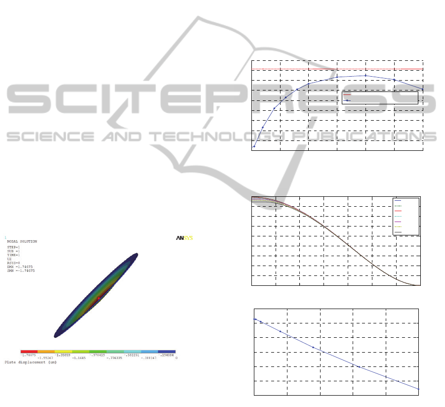
Figure 3: Screenshot of membrane with pyramid.
Pyramids on the membrane have been modelled
to have: a) the same size but locations all along a
radius of the membrane; and b) different sizes on the
same position in the centre of the membrane. An
example of a membrane with a pyramid, deflected
under the applied pressure, is given in Fig. 3. The
different colours are different regions of deflection
of the membrane.
Fig 4 shows the simulations of the displacement
of the center point of the membrane (maximum
deflection) in relation to different locations of a
pyramid (base side: 30 μm) over the radius line of
the membrane. We can highlight the significant drop
in displacement when the pyramid is located close to
the center of the membrane. Therefore the strongest
impact of a pyramid is produced at that location. If a
pyramid is located closer to the edge of the
membrane, the influence on the deflection gets
smaller. However second order effects related to the
proximity to the clamped edge and variations in the
effective geometry of the membrane (areas of
maximum stress) make the maximum deflection to
decrease, contrary to what could be expected, for
pyramids approaching the edge of the membrane.
Figure 4: Center deflection vs pyramid location.
Figure 5: Deflection for pyramids located at the center.
The next step is to place the pyramid in the
center of the membrane while only its size is varied.
The base length of the pyramids has been varied in
the range from 5 to 50 μm. The simulation results
are shown in Fig. 5. As can be seen in the lower
graph, the displacement of the centre point of the
0 50 100 150 200 250 300
1.745
1.75
1.755
1.76
1.765
1.77
1.775
1.78
1.785
1.79
Center Distance (um)
Max. Displacement (um)
Center Displacement vs. Pyramid Distance to the Center of the Plate (@P=8kPa)
DEFLECTION W/O. PYR
DEFLECTION W/. PYR (30x30)um
2
0 50 100 150 200 250 300 350
0
0.2
0.4
0.6
0.8
1
1.2
1.4
1.6
1.8
Distance
(
um
)
Deflection (um)
Membrane Deflection vs. Pyramid Base Area (@P=8kPa)
PYR0U
PYR5U
PYR10U
PYR20U
PYR30U
PYR40U
PYR50U
0 500 1000 1500 2000 2500
1.68
1.7
1.72
1.74
1.76
1.78
1.8
Center Displacement vs. Pyramid Base Area (@P=8kPa)
Base Area (um
2
)
Max. Displacement (um)
AnalysisofFaultInjectioninImplantableCapacitiveBlood-pressureSensors
157

membrane approximates a linear function, as it
steadily decreases with increasing pyramid size. The
upper graph in Fig. 5 shows the membrane
deflection for different pyramid sizes. One important
aspect to point out is the constant maximum
deflection value for the membrane, not at a single
point, but under the complete pyramid base area.
This last effect cannot be modelled by using the
mathematical formulation presented in Section 3,
even if we modify it to increase its accuracy in order
to get closer to the results obtained by FE analysis.
Fig. 4 and Fig. 5 also show that the presence of a
pyramid on top of the membrane of our capacitive
MEMs pressure sensor produces a smaller deflection
than expected in the fault-free case. Thus, this faulty
condition implies a sensitivity loss of the sensor that
can compromise its reliability, which is a critical
issue for implantable devices.
Therefore, it is important to count on an accurate
behavioural model for its main component, the
membrane, valid for both fault-free and faulty
conditions. As said before, its deflection can have an
acceptable analytical solution in the fault-free case.
However, in this work we have proven that this
mathematical formulation is no longer valid for
modelling the membrane with certain kinds of faults
as, for example, the formation of pyramids on top of
the membrane. Therefore it is necessary to create
additional mathematical models that accurately
describe the behaviour of the membrane under faulty
conditions, considering the deflection results
obtained through FE simulations. Especially for
those faulty cases which significantly affect the
geometry and/or material properties of the
membrane.
5 CONCLUSIONS
In this work test-related problems for implantable
capacitive MEMS pressure sensors for the early
detection of in-stent restenosis have been presented.
The typical failure mechanisms and defects that can
give raise to the faulty behaviour of a
microelectromechanical system have also been
explained.
The deflection problem of circular membranes
has been proven to be analytically or numerically
solvable for a fault-free case, in order to build a
behavioural model of the sensor. Nevertheless, this
mathematical model is not valid to describe certain
faulty conditions where the geometry or the material
properties of the membrane are seriously affected.
So as to obtain a realistic fault model in these cases a
finite-element analysis must be performed.
REFERENCES
Castillejo A., Veychard D., Mir S., Karam J., Courtois B.,
Failure Mechanisms and Fault Classes for CMOS-
Compatible Microelectromechanical Systems, IEEE
International Test Conference, pp. 541–550, 1998.
Chang S.-P., Lee J.-B., Allen M.G., Robust capacitive
pressure sensor array, Sensors and Actuators A:
Physical, vol. 101, pp. 231–238, September 2002.
Huang Y., Vasan A. S. S., Doraiswami R., Osterman M.,
Pecht M., MEMS Reliability Review, IEEE
Transactions on Device and Materials Reliability, vol.
12, no. 2, pp. 482-493, June 2012.
Landsberger L. M., Nashed S., Kahrizi M., Paranjape M.,
On Hillocks Generated During Anisotropic Etching of
Si in TMAH, Journal of Microelectromechanical
Systems, vol. 5, no. 2, pp. 106-116, 1996.
Mir S., Charlot B., Courtois B., Extending Fault-Based
Testing to Microelectromechanical Systems, Journal
of Electronic Testing: Theory and Applications, vol.
16, pp. 279–288, 2000.
Mukherjee T., Fedder G. K., Blanton R. D., Hierarchical
design and test of integrated microsystems, IEEE
Design and Test of Computers, vol. 16 (4), pp.18–27,
1999.
OECD (2010), Health at a Glance: Europe 2010, OECD
Publishing. http://dx.doi.org/10.1787/health_glance-
2010-en
Rosing R., Reichenbach R., Richardson A., Generation of
component level fault models for MEMS,
Microelectronics Journal, vol. 33, pp. 861–868, 2002.
Takahata K., Gianchandani Y. B., Wise K. D.,
Micromachined antenna stents and cuffs for
monitoring intraluminal pressure and flow, Journal of
Microelectromechanical Systems, vol 15(5), pp. 1289–
1298, October 2006.
Teegarden D., Lorenz G., Neul R., How to model and
simulate microgyroscope systems, IEEE Spectrum 35
(7), pp. 66–75, 1998.
Timoshenko S., Theory of Plates and Shells, McGraw-
Hill, New York, 1940.
Wang L-T., Stroud C. E, Touba N. A., System-on Chip
Test Arquitectures. Nanometer Design for Testability,
1st. ed., Elsevier: Morgan Kaufmann Series, 2008.
BIODEVICES2013-InternationalConferenceonBiomedicalElectronicsandDevices
158
