
Hardware-software Scalable Architectures for Gaussian Elimination
over GF(2) and Higher Galois Fields
Prateek Saxena, Vinay B. Y. Kumar, Dilawar Singh, H. Narayanan and Sachin B. Patkar
Department of Electrical Engineering, Indian Institute of Technology Bombay, Mumbai, India
Keywords:
Galois Field Matrix Computations and Linear Equation Solvers, GF(2), Block Gaussian Elimination with
Pivoting over GF(2), Hardware/Software Co-design, Custom Processor Extensions.
Abstract:
Solving a System of Linear Equations over Finite Fields finds one of the most important practical applica-
tions, for instance, in problems arising in cryptanalysis and network coding among others. However, other
than software-only approaches to acceleration, the amount of focus particularly towards hardware or hard-
ware/software based solutions is small, in comparison to that towards general linear equation solvers. We
present scalable architectures for Gaussian elimination with pivoting over GF(2) and higher fields, both as
custom extensions to commodity processors or as dedicated hardware for larger problems. In particular, we
present: 1) Designs of components—Matrix Multiplication and ‘Basis search and Inversion’—for Gaussian
elimination over GF(2), prototyped as custom instruction extensions to Nios-II on DE2-70 (DE2, 2008), which
even with a 50MHz clock perform at ≈30 GOPS (billion GF(2) operations); and also report results for GF(2
8
)
or higher order matrix multiplication with about 20 GOPS performance at 200MBps. 2) A scalable extension
of a previous design (Bogdanov et. al, 2006) for multiple FPGAs and with ≈2.5 TrillionOPS performance at
5GBps bandwidth on a Virtex-5 FPGA.
1 INTRODUCTION
Several algorithms have been proposed and imple-
mented to solve a system of linear equations (SLE’s)
over Galois fields (GF) in polynomial time(Rupp
et al., 2011; Bogdanov and Mertens, 2006; Wang and
Lin, 1993; Parkinson and Wunderlich, 1984; Koc¸ and
Arachchige, 1991). The most commonly used algo-
rithm is Gaussian elimination which has O(n
3
) com-
plexity where n is number of variables in the linear
system.
Solution of SLE over GF(2) have a special rele-
vance since they are so often encountered in cryp-
tography among others (e.g. (Ditter et al., 2012)).
As cited in(Bogdanov and Mertens, 2006) many ci-
phers can be represented as finite state machines over
binary fields, where every output bit can be written
as non/linear functions of input and key bits, and
the system can be solved using SLE solvers, post-
linearization, if necessary. One of the more direct
applications is in factorization using the general num-
ber field sieve (GNFS) algorithm, where, for instance,
factoring a 120 digit number deals with an SLE of
size 10
6
× 10
6
, further emphasizing the relevance of
this effort. The other motivation for the presented
hardware/software (HW-SW) approach is the partic-
ular inefficiency of mainstream computing infrastruc-
ture (general purpose processors, GPUs) for finite-
field computations as the mainstream requirement is
for floating point operations.
1.1 Organization
In section 2, we present architectures suitable for HW-
SW co-design or as custom processor extensions. In
particular, the subsections describe architectures for
“Basis search and Inversion”, and a “32 × 32bit ma-
trix multiplier”, both to be used as components facil-
itating Gaussian elimination over GF(2) (in 32 × 32
blocks). An approach for matrix multiplication over
higher galois fields, based on adapting existing float-
ing point architectures, is also reported.
Section 3 describes, a scalable extension of Bog-
danov et. al’s design, presented as a dedicated hard-
ware design for larger problems.
2 CUSTOM PROCESSOR
EXTENSIONS FOR CO-DESIGN
This section describes fast and efficient architectures
195
Saxena P., B. Y. Kumar V., Singh D., Narayanan H. and B. Patkar S..
Hardware-software Scalable Architectures for Gaussian Elimination over GF(2) and Higher Galois Fields.
DOI: 10.5220/0004313201950201
In Proceedings of the 3rd International Conference on Pervasive Embedded Computing and Communication Systems (PECCS-2013), pages 195-201
ISBN: 978-989-8565-43-3
Copyright
c
2013 SCITEPRESS (Science and Technology Publications, Lda.)
for operations over GF(2) that are good candidates as
light weight extensions to commodity embedded pro-
cessors, e.g. NIOS-II. One apt use could be with spe-
cial purpose custom processors to facilitate fast so-
lutions of boolean equations. These extensions are
‘light weight’ in the sense that they do not require any
modifications to the standard memory access datap-
ath (typically, 32-bit wide); also, the resource usage
of these components, say, in particular, the 32 × 32
bit matrix multiplier block, is comparable to that of a
pipelined floating point unit.
Algorithm 1 describes block gaussian elimination.
Considering 32 × 32 bit sized blocks for the GF(2)
case, we present hardware architectures for matrix
transpose and multiplication over GF(2) and a mod-
ule for basis search and inversion for pivoting.
Algorithm 1: Block Gaussian Elimination over
GF(2).
Data: Matrix A ∈ {0, 1}
n×n
for i=0 to B-1 do
A
−1
[i, i] ←−
BuildBasisPermuteInvert(A[i:B-1,i])
for k = i+1 to B-1 do
A
i,k
←− A
−1
i,i
A
i,k
end
for j=i+1 to B-1 do
for k=i+1 to B-1 do
A
j,k
←− A
j,k
⊕A
j,i
A
i,k
end
end
for j = i+1 to B-1 do
MakeZero(A
j,i
)
end
end
As evident from Algorithm. 1, whereas the GF(2)
32 × 32 bit matrix (uint32 t A[32]) additions are
cheap on any general purpose processor, the bulk of
the time, however, is spent around matrix multipli-
cation, and once per diagonal block, in basis-search
and inversion. Based on this observation, the more
natural manifestation of this idea would be a cus-
tom hybrid HW-SW system with simple and mini-
mal processors together with these custom extensions,
with the cheaper ‘add’ operations and ‘flow-control’
running on the processors. Further, with access to
open-source high-level synthesis tools—in particular,
LegUp(Canis et al., 2011), specializing in proces-
sor/accelerator platform generation—conceiving and
realizing such hybrid HW-SW based FPGA designs
is now possible, albeit with some more work.
However, as a proof of concept the three com-
ponents have been prototyped on DE2-70 board as
Figure 1: 32 × 32 GF(2) Transpose.
32
32
32
T
A[i][1]
32
3232
A[i][30]
T
32
32
T
A[i][31]
32
32
32
32
32
A[i][0]
T
32
ZERO
32
32
XOR
B[i]
B[i]
B[i]
B[i]
LoadSide
LoadSide
LoadSide
LoadSide
Result
LoadTop
LoadDown
SEL
AND
AND
AND
AND
Figure 2: Outerproduct accumulation.
custom instruction extensions to NIOS-II, where,
although the 50MHz clock is a limiting factor, as the
results suggest, it still makes a compelling case. The
interface to the custom instruction used is:
module X Custom Instruction (clk, reset,
clk en, dataa, n, result, start, done);
where dataa, n, and result ports are 32, 8 and 32
bit wide respectively.
2.1 Matrix Multiplication over GF(2)
The product(AB) of matrices A, B:
A = [c
0
c
1
. . . c
n
] and B = [r
0
;r
1
;. . . r
n
]
where c
i
’s and r
i
’s denote the columns and rows re-
spectively, can be thought of as
AB =
n−1
∑
i=0
c
i
r
i
where the outerproducts c
i
r
i
are accumulated to form
the result. Figure 2 illustrate a fast 32 × 32 bit matrix
PECCS2013-InternationalConferenceonPervasiveandEmbeddedComputingandCommunicationSystems
196

multiplication (uint32 A[32], B[32]) architecture,
composed of a 32 bit Matrix Transpose unit and an
Outerproduct accumulator unit. The design com-
pactly uses O(n
2
) resources—registers: 2n
2
; XOR,
AND: n
2
—so that one outerproduct computation and
accumulation happens each clock.
32 words (each 32 bit wide) of A are sent first, fol-
lowed by, 32 words of B, at the end of which the result
is completely available. The Transpose unit (Figure
1) circularly rotates the columns of its input matrix
making it suitable/reusable for cases where a series
of matrix multiplications needs to be done with the
same matrix, e.g., when scaling rows during the elim-
ination.
The design uses 2096 slices on a 5vlx50tff1136-2
(or 7% of the device), 98% of which are completely
utilized, and runs at 551MHz. It is also scalable, as
expected, from the regular arrangement of resources
and routing for the architecture.
On the 50 MHz DE2-70 FPGA platform, the
speed-up due to the custom instruction compared to
a equivalent soft 32 ×32 GF(2) matrix multiplier run-
ning on NIOS-II is about 30×.
2.2 Basis Search and Inversion
For the following discussion we inductively assume
that the row elimination process has completed to
some intermediate stage, where i − 1 tiles along the
diagonal starting from the tile A
1,1
have been inverted
(after row permutations as necessary). This leaves
us with the submatrix with A
i,i
as the first diagonal
tile. We do a partial pivoting (permuting rows) such
that after appropriate row permutations, the tile A
i,i
becomes invertible. Note that each tile is a 32 × 32
matrix with elements from GF(2), and we are seek-
ing to find 32 linearly independent rows (each GF(2)
elements) from among the 32 × (B − i) rows in the
lower portion of the i
th
column of tiles—the diagonal
tile and downwards. So, searching within the rows
of A
i,i
, A
i+1,i
, . . . A
B−1,i
, we find a set that forms a ba-
sis (for that i
th
column matrix), while also permut-
ing the rows so as to form an invertible A
i,i
. This has
been efficiently implemented in hardware, the archi-
tecture for which is described next, where, both the
basis search and inversion of the diagonal tile are ef-
ficiently done in lock-step.
We maintain an array PB of 32 registers of 32 bits
each (reg [31:0] PB[0:31]), for storing and building a
partial basis (PB, pbasis) of the rows of A[i : B − 1, i]
(denoting the column-i tiles of the current submatrix
under process). The algorithm needs to process all
32× (B −i) rows in the worst case for testing whether
a given candidate row (CR) can be augmented to the
PB[0]
LNZ
/
32
isZero
1
0
/
32
/
32
/
32
/
32
0
/
32
/
32
PB[k]
LNZ
/
32
isZero
1
0
/
32
/
32
/
32
/
32
0
/
32
/
32
PB[31]
LNZ
/
32
isZero
1
0
/
32
/
32
/
32
/
32
0
/
32
/
32
.
.
.
.
.
.
XOR tree
REDUCED CR
1
0
0
/
32
/
32
isZero
+
/
32
PB[k]
/
32
/
32
LNZ
/
32
/
32
+
CR
REDUCED CR
1
0
isZero
PB[count]
0
/
32
/
32
/
32
/
32
/
32
/
32
/
32
/
32
Figure 3: Datapath for Basis Search and Inverse (not
shown).
partial basis built so far, a count of which is kept by
register ‘count’(reg [4:0] count). The 32 bit wide state
registers PB[0], PB[1], . . . PB[count] contain the row-
reduced versions of the set of rows included in the
partial basis (at t=count cycles), and the rest of the
PB[count + 1]. . . PB[31] stay in their zero initialized
state. The array of wires [31:0] PB LNZ [0:31] are
used to characterize the ‘Leading Non Zero’ of each
of the PB, which carry a ‘1’ in the place of the LNZ.
The LNZ module, combinational block, is essentially
a priority encoder. This has been recursively defined
in terms of 4x4 priority encoders to balance the worst
case delay.
Inductively the following structure of reduced
rows is maintained inside the partial basis array PB.
Any column that contains a leading nonzero of one of
the rows of pbasis contains ‘0’ in all other locations,
and when we finish finding our 32 rows forming the
basis, the PB array holds a row permuted identity ma-
trix while the inverse PB Inv is also ready in another
set of registers. The following pseudo-verilog de-
scription captures the essential details, together with
Figure 3.
//COMBINATIONAL (next state logic)
#pragma parallel
for(i=0; i<32; i=i+1)
if(PB_LNZ[i] & CR) {
PB_tobe_XORed[i] = PB[i];
PB_Inv_tobe_XORed[i] = PB_Inv[i];
}else{
PB_tobe_XORed[i] = 0;
PB_Inv_tobe_XORed[i] = 0;
}
reduced_CR = XOR_Tree(CR,
PB_tobe_XORed<0,1,..31>);
if(reduced_CR != 0) {
PB_next[count] = reduced_CR;
Hardware-softwareScalableArchitecturesforGaussianEliminationoverGF(2)andHigherGaloisFields
197

PB_Inv_next[count] =
XOR_Tree(PB_Inv[count],
PB_Inv_tobe_XORed<0,..31>);
#pragma parallel
for(i=0; i<count; i=i+1) {
if(reduced_CR_LNZ & PB[i]) {
PB_next[i] =
PB[i] ˆ reduced_CR;
PB_Inv_next[i] =
PB_Inv[i] ˆ PB_Inv_next[count];
}
}
}
//SEQUENTIAL (state update)
#on posedge clock
PB[i] <= PB_next[i]
PB_Inv[i] <= PB_Inv_next[i]
Note that the permuted identity matrix in PB (en-
coded to (reg [4:0]) 0→31) together with PB Inv can
be easily used to recover A
−1
i,i
.
2.3 Matrix Multiplication over GF(2
q
)
For large matrix multiplication problems over higher
Galois fields (GF(2
q
)), the approaches discussed so
far, tailored for GF(2), would not be appropriate. One
approach we propose here is to adapt existing litera-
ture on handcrafted designs for general matrix mul-
tiplication to GF matrix multiplication. The archi-
tecture in (Kumar et al., 2010) describes an efficient
and scalable design for double precision matrix mul-
tiplication under the constraints of limited bandwidth.
We adapt the design to do GF(2
8
) matrix multiplica-
tion which was implemented and validated on Nallat-
ech BenOne board(ben, 2008), a HW-SW co-design
platform. The adaptation was essentially in terms
of reusing the same datapath but with GF(2
8
) mul-
tiplier/accumulators replacing the double precision
units. The prototype design (unoptimized), clocking
at 200MHz, gives a performance of ≈20 GOPS (20
billion GF(2
8
) operations per second), at a low band-
width requirement of around 200MBps. This was us-
ing just one of the four available PCIe channels to the
board.
Using the same 64-bit wide datapath as in the orig-
inal design (for double precision floating point), and
the additional unused bandwidth available over the
PCIe, the performance would easily scale to 80GOPS,
with 4 GF(2
8
) operations in place of 1, which also
amounts to using the architecture’s FPGA specific re-
sources/datapath more efficiently.
3 DEDICATED HARDWARE
ARCHITECTURE FOR SLE
OVER GF(2)
This sections describes a natural extension of an SLE
architecture over GF(2) as proposed in (Bogdanov
and Mertens, 2006), for multiple FPGAs.
3.1 Bogdanov’s Approach
The algorithm proposed in (Bogdanov and Mertens,
2006), which we briefly summarize here as a precur-
sor to the next section, is a variation of the LU factor-
ization method. After doing the elementary row and
column operations, the resultant matrix is the identity
matrix instead of Upper triangular. The underlying
principle of their approach is data movement in two
atomic operations, which the authors call—1. Shiftup
and 2. Elimination.
The shiftup operation cyclically shifts the unused
rows up by one if the element of the top most row
and that of the column under consideration is found
equal to zero. The used rows are not touched. The
eliminate operation performs elementary row opera-
tion when the pivot is non-zero. Once the required
operations are done, the entire matrix is shifted up
and left, so as to ensure that the next pivot element
is in place. In essence, the eliminate operation does
two things: Row elimination and row shifting.
The new algorithm can now be represented in
terms of these two basic operations as Algorithm 2.
Algorithm 2: Modified Gaussian Elimination over
GF(2).
begin
Data: Matrix A ∈ {0, 1}
n×n
appended with
vector b
Result: Matrix {x|I}
for each column k=0 to n-1 do
while a
1,1
= 0 do
A = Shift-up(n-k+1, A);
end
A = Eliminate(A);
end
end
The architecture for the algorithm uses a mesh
structure (Figure 5) consisting of an interconnection
of four cell types of cells—1. Pivot, 2. First Row, 3.
First Column, and 4. Common.
Each cell corresponds to an entry of the matrix
{A|b} (over GF(2)). The entries of the matrix are
moved as per the Shiftup and Eliminate operations
and thus the individual ‘cells’ contain the state of the
PECCS2013-InternationalConferenceonPervasiveandEmbeddedComputingandCommunicationSystems
198

matrix at any given time. Each cell uses some mul-
tiplexing logic and a 1-bit register for state. The first
column cell uses an extra one bit register for the ‘flag’
status for that particular row. Each cell in the mesh is
connected to the cells vertically and diagonally above
and below it via local signals, and also to the leftmost
cell, the topmost cell and the first cell of the matrix via
global signals. The leftmost cell is defined as the cell
which contains the entry of the column under consid-
eration. The topmost cell is defined as the cell which
contains the corresponding entry of the row which is
supposed to do the Shiftup or the Eliminate operation.
The first cell of the matrix is defined as the one which
contains the topmost entry of the column under con-
sideration i.e., the pivot cell.
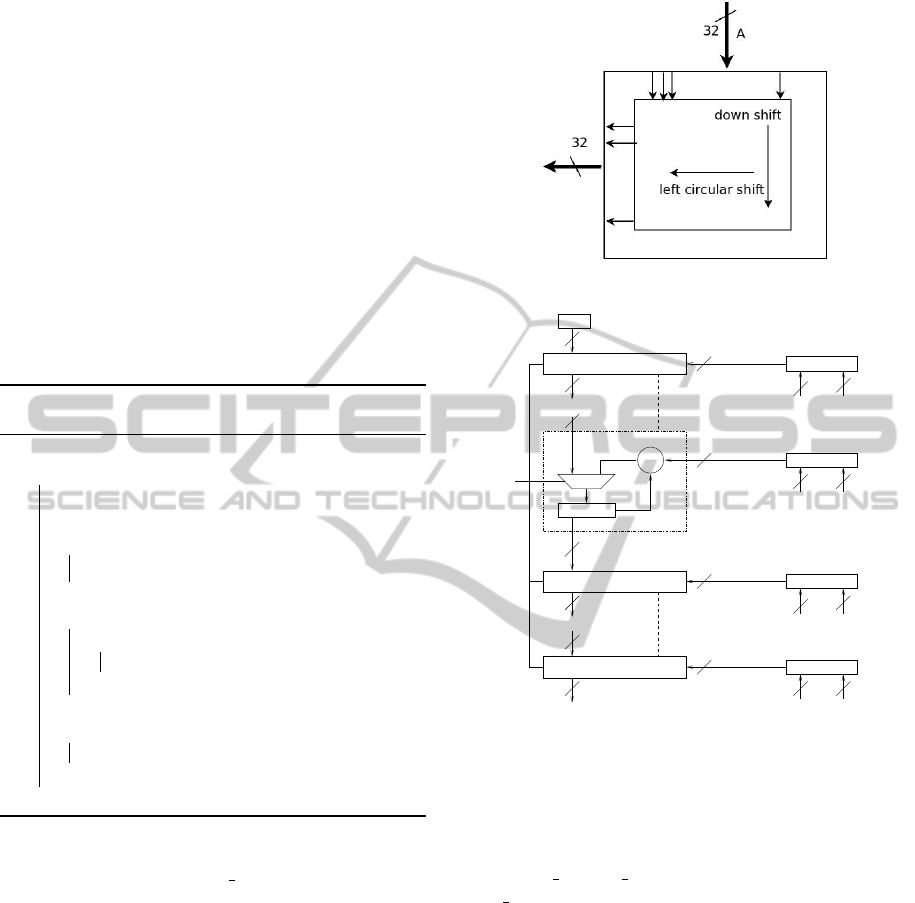
The direction of data transfer during the Shiftup
operation is shown in Figure 4. The unconnected
blocks at the bottom refer to the locked rows which
do not participate in the Shiftup operation. The mesh
structure is in effect transformed into a toroidal mesh
structure due to the cyclic nature of the operations
involved. The direction of data transfer during the
Eliminate operation is shown in Figure 5.
FCC
FCC
FCC
FRC FRC FRC
CC
CC CC
CC CC
CC
CC CC CC
PIVOT
USED
ROW
Figure 4: Shiftup.
FCC
FCC
FCC
PIVOT
FRC FRC FRC
CC CC CC
CC
CCCC
CC
CC CC
LAST
TO
FIRSTFROM
Figure 5: Eliminate.
3.2 Extension of Bogdanov’s Approach
The maximum size of a SLE (over GF(2)) that can
be solved on a Virtex 5 FPGA using Bogdanov’s ap-
proach is around 90 × 90, essentially limited by the
number of slices on the device. One method to ex-
tend the size of SLE that can be handled is by parti-
tioning the matrix and by simultaneous execution on
a multi-FPGA system. The modularity inherent in the
algorithm allows us to easily extend the idea to matri-
ces of larger sizes. The entire matrix is partitioned
into tiles. Each core now holds one tile. In order
to make the same algorithm work on a multi-FPGA
system certain data has to be communicated across
the tiles. As a natural extension to the architecture
proposed by Bogdonov et. al., a simple partitioning
scheme is proposed and the idea is validated on a sin-
gle Virtex-5 FPGA board.
The equation matrix A ∈ {0,1}
N×N
appended with
column vector b ∈ {0,1}
N×1
is partitioned into
N
B−1
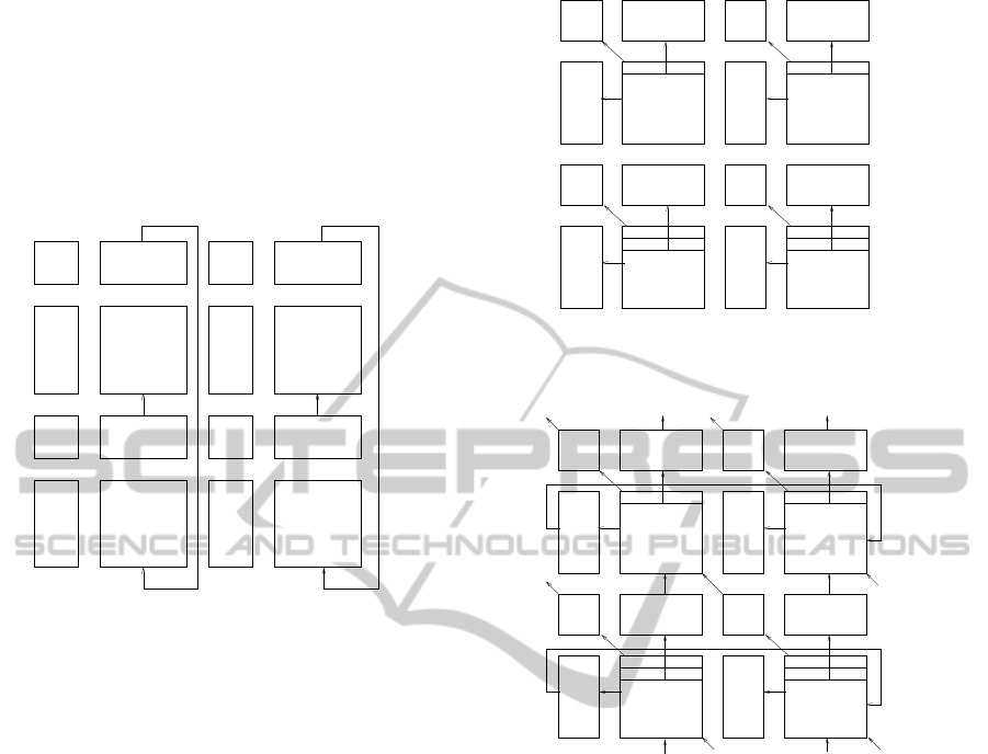
2
TRT TRT TRT
CT
CT CT
CT
CT
CT
TRT : TOP ROW TILE
CT : COMMON TILE
Figure 6: Tile Arrangement.
tiles of size B × B. The composition of each tile is
same as that of Figure 4. Each FPGA on a multiple
FPGA setup can hold one such tile. The tile arrange-
ment is shown in Figure 6.
The tiles are of two types–1. Top Row Tile, 2.
Common Tile. The top row tiles are different from the
other tiles since the top row is being used for Shiftup
and Eliminate operations. Intermediate buffers are
required for communicating this information across
tiles. During the Eliminate operation when the di-
agonal up shifting is happening, then data has to
be moved across tiles. To facilitate this movement,
buffers are used. These buffers are used to indicate
the data that has to be transferred, i.e., they indicate
the data movement. This data movement can be han-
dled as desired depending upon the platform used.
Currently, since this design is being tested on a sin-
gle FPGA, buffers are used. The arrangement of the
buffers and the tiles is shown in Figures 7, 8.
Corresponding to each tile there is a Horizontal
Buffer, a Vertical Buffer and a Diagonal Buffer. The
Horizontal buffer has width equal to the number of
columns in the Tile. The length of the vertical buffer
is equal to the number of rows in each tile. The diag-
onal Buffer is a one bit register to store the diagonal
value.
Each tile performs the Eliminate and Shiftup oper-
ation independently. The topmost horizontal buffers
are connected to the all the tiles in the same column.
The topmost row of every tile is copied from its top-
most horizontal buffer after every Eliminate or Shiftup
operation. This ensures that each tile uses the same
row for elimination. The topmost horizontal buffer is
fed by the top most row of the Top Row Tile. Other
horizontal buffers are fed from the second row of the
Common tile.
Similarly each tile is connected to the leftmost
vertical buffer. The leftmost vertical buffer is differ-
ent from other buffers since it stores two values—the
value of the leftmost column of the leftmost tile and
also the value of ‘used’ flag for that entire row dis-
tributed among the various tiles. The connection of
each tile to the leftmost vertical buffer is to ensure
Hardware-softwareScalableArchitecturesforGaussianEliminationoverGF(2)andHigherGaloisFields
199
that the correct xor is being done and to obtain the
value of the lock.
A simplified version consisting of four tiles is
shown to explain the data movement. The data move-
ment during the Shiftup operation is shown in Figure
7. After the data has been shifted vertically up, the
buffers have to be reloaded to indicate the new val-
ues. This is done after every Shiftup.
HB : HORIZONTAL BUFFER
VB : VERTICAL BUFFER
DE : DIAGONAL ENTRY
TRT : TOP ROW TILE
CT : COMMON TILE
VB 1
DE 3
VB 3
HB 1DE 1
TRT A
DE 2
HB 2
TRT B
HB 4
CT B
DE 4
VB 4
CT A
HB 3
VB 2
Figure 7: During Shiftup.
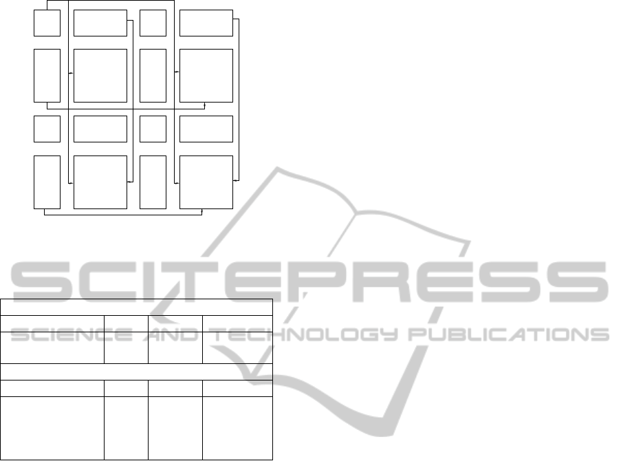
Once the data is moved vertically, the buffers are
updated. This is shown in Figure 8.
The data movement during the Eliminate oper-
ation is shown in Figure 9. Here the buffers are
reloaded simultaneously, hence there is no need of a
separate buffer loading stage.
In addition to the above mentioned buffers, there
are the signals (Figure 9) GlobalAdd, LeftColumnVal,
TopRowVal and RowLockVal.
GlobalAdd is the output of the top most diagonal
buffer. In the above example, the output of the DE1
is the GlobalAdd. This is needed by each tile to de-
termine whether to perform the Shiftup or the Elimi-
nate operation. LeftColumnVal consists of the outputs
from the leftmost vertical buffers. The left most verti-
cal buffers as stated hold the values of the first column
of the leftmost tile. This is needed to figure out if the
elementary row operation needs to be done on a par-
ticular row or not. TopRowVal consists of the outputs
of the topmost Horizontal Buffer. The topmost hor-
izontal buffer holds the value of the row performing
the elementary row operation. Hence this row is fed to
each of the tile which then performs the necessary op-
eration. The RowLockVal is generated from the used
flag of present in the first column of the first column
of tiles. They help us to keep track of which rows have
been used and which are unused (for elementary row
HB : HORIZONTAL BUFFER
VB : VERTICAL BUFFER
TRT : TOP ROW TILE
CT : COMMON TILE
DE : DIAGONAL ENTRY
VB 1
DE 3
VB 3
HB 1DE 1
TRT A
DE 2
HB 2
TRT B
HB 4
CT B
DE 4
VB 4
CT A
HB 3
VB 2
Figure 8: Reloading Buffers After Shiftup.
HB : HORIZONTAL BUFFER
VB : VERTICAL BUFFER
DE : DIAGONAL ENTRY
TRT : TOP ROW TILE
CT : COMMON TILE
VB 1
DE 3
VB 3
HB 1DE 1
TRT A
DE 2
HB 2
TRT B
HB 4
CT B
DE 4
VB 4
CT A
HB 3
VB 2
TO CT B TO CT A TO CT A TO CT B
FROM DE 3
TO TRT B
FROM DE 2
FROM HB 1
FROM DE 1
FROM HB 2
Figure 9: During Eliminate.
operations). These connections are shown in Figure
10.
This interconnection architecture was tested on
the Xilinx Virtex 5 FPGA. Different matrix sizes with
different block tile ratio were tested. The results ob-
tained were verified to be correct. The worst case time
taken in this case also comes out to be quadratic.
3.3 Preliminary Results
The following is an evaluation of the above architec-
tures (both, a port of the original, and the proposed
extension) on Xilinx Virtex 5 FPGA. In Table 1 ‘5 × 5
of 10 × 10’ represents a 5 × 5 arrangement of tiles
of dimension 10 × 10. The table indicates that the
slices/cell ratio does not increase much over various
interconnection schemes. The design clock frequency
(here 595MHz) is comparable to the original design,
however, it will naturally be limited by the chip-to-
chip interconnection on an actual multifpga setup.
PECCS2013-InternationalConferenceonPervasiveandEmbeddedComputingandCommunicationSystems
200
HB : HORIZONTAL BUFFER
VB : VERTICAL BUFFER
DE : DIAGONAL ENTRY
TRT : TOP ROW TILE
CT : COMMON TILE
VB 1
DE 3
VB 3
HB 1DE 1
TRT A
DE 2
HB 2
TRT B
HB 4
CT B
DE 4
VB 4
CT A
HB 3
VB 2
GLOBAL_ADD
LEFT_ROW_VAL, ROW_LOCK_VAL
LEFT_ROW_VAL, ROW_LOCK_VAL
TOP_ROW_VAL
TOP_ROW_VAL
Figure 10: Global Connections.
Table 1: Comparison validating the scalability.
Bogdanov’s architecture
size cells slices slices/cell
50×50 2500 5337 2.13
70×70 4900 10,684 2.18
Proposed Extended architecture
size cells slices slices/cell
5×5 of 10×10 2500 5184 2.07
7×7 of 10×10 4900 12,593 2.57
10×10 of 5×5 2500 5,507 2.21
10×10 of 7×7 4900 13,137 2.68
4 CONCLUSIONS
We present hardware building blocks, in a hard-
ware/software codesign solution, for solving large
system of linear equations (SLE) over Galois fields.
For SLEs over GF(2), an important special case, we
present efficient architectures for—a. basis search and
inversion (for tile-based Gaussian elimination), and b.
32 × 32 bit matrix multiplication. Prototyping these
as custom instruction extensions to NIOS-II, we ar-
gue the case for the use of the designs as light weight
extensions to custom or commodity processors for
relevant applications. We see that even when lim-
ited by the 50MHz clock on DE2-70 FPGA board,
the co-design solution can perform at ≈30GOPS. For
large matrix multiplication over GF(2
8
), we present
an adaptation from an earlier reported architecture for
64-bit floating point matrix multiplication. For large
SLE over GF(2), we also present an extension of Bog-
danov’s design, scalable over multiple FPGAs, along
with validating preliminary results indicating over 2.5
Trillion GF(2) operations on a Virtex-5 device.
ACKNOWLEDGEMENTS
The authors sincerely acknowledge Naval Research
Board (NRB), India (Project No. NRB-202/SC/10-
11) and Intel India Research Council for the financial
support covering this work.
REFERENCES
(2008). Altera DE2-70 - Development and Education
Board. Terasic.
(2008). Nallatech BenOne Board. Nallatech.
Bogdanov, A. and Mertens, M. C. (2006). A Parallel Hard-
ware Architecture for fast Gaussian Elimination over
GF(2). In Proceedings of the 14th Annual IEEE Sym-
posium on Field-Programmable Custom Computing
Machines, FCCM ’06, pages 237–248, Washington,
DC, USA. IEEE Computer Society.
Canis, A., Choi, J., Aldham, M., Zhang, V., Kammoona,
A., Anderson, J. H., Brown, S., and Czajkowski, T.
(2011). Legup: High-level synthesis for fpga-based
processor/accelerator systems. In Proceedings of the
19th ACM/SIGDA international symposium on Field
programmable gate arrays, FPGA ’11, pages 33–36.
ACM.
Ditter, A., Ceska, M., and Luttgen, G. (2012). On Parallel
Software Verification Using Boolean Equation Sys-
tems. In SPIN, pages 80–97.
Koc¸, c. K. and Arachchige, S. N. (1991). A fast algorithm
for Gaussian elimination over GF(2) and its imple-
mentation on the GAPP. J. Parallel Distrib. Comput.,
13(1):118–122.
Kumar, V. B. Y., Joshi, S., Patkar, S. B., and Narayanan,
H. (2010). FPGA Based High Performance Double-
Precision Matrix Multiplication. International Jour-
nal of Parallel Programming, 38(3-4):322–338.
Parkinson, D. and Wunderlich, M. (1984). A compact al-
gorithm for gaussian elimination over GF(2) imple-
mented on highly parallel computers. Parallel Com-
put., 1(1):65–73.
Rupp, A., Eisenbarth, T., Bogdanov, A., and Grieb, O.
(2011). Hardware SLE solvers: Efficient build-
ing blocks for cryptographic and cryptanalyticappli-
cations. Integration, 44(4):290–304.
Wang, C.-L. and Lin, J.-L. (1993). A Systolic Architecture
for Computing Inverses and Divisions in Finite Fields
GF(2
m
). IEEE Trans. Comput., 42(9):1141–1146.
Hardware-softwareScalableArchitecturesforGaussianEliminationoverGF(2)andHigherGaloisFields
201
