
Far-field Scatter Measurements of Planar Optical Waveguides using
a Variable Launch System
Robert Ferguson, Irshaad Fatadin, Subrena Harris and James Allerton
National Physical Laboratory, Teddington, Middlesex, TW11 0LW, U.K.
Keywords:
OPCB, Waveguides, Far-field.
Abstract:
Polymer planar optical waveguides fabricated onto electrical printed circuit boards are an emerging technology
to provide high-speed communications on computer backplanes. Along with the key parameters of attenuation
and isolation, the variable launch system developed at NPL can now be used to measure the transmitted scatter
profile of optical printed circuit boards (OPCBs) in order to explore the relationship between launch condition,
waveguide and end-face quality. In this paper we describe the modifications to the existing NPL system and
measurements of the far-field intensity profiles of a group of reference waveguides using a variety of spot sizes
and numerical apertures.
1 INTRODUCTION
Polymer planar optical waveguides fabricated onto
electrical printed circuit boards and incorporated onto
computer backplanes are an emerging cost effective
technology to facilitate high-speed data transfer in
modern high speed computing and data storage sys-
tems. The integrated manufacture of these OPCBs has
been investigated (Selviah, 2008, Bamiedakis, 2012)
and is being further refined with demonstrators cur-
rently operating >10 Gb/s. Their bandwidth capac-
ity, size and lower energy demands ensure continuing
interest among the leading international communica-
tions companies. Along with the technical demands
of fabricating the boards or backplanes, a need to
characterise the actual guides themselves is also es-
sential. The optical performance of the waveguides
is an important aspect to refining the manufacturing
process (Kai Su, 2005). Currently these waveguides
are multimoded, operating at 850 nm and intended for
very high data rates. In addition to the fundamen-
tal parameters of attenuation and isolation, there is
a need to understand the losses associated with the
end-face surfaces and waveguide quality. An estab-
lished system at NPL already measures the attenua-
tion and isolation from the transmitted power and has
the ability to vary the launch spot size and numerical
aperture to fully explore the capability of these multi-
mode waveguides (Ferguson, 2012). This system has
now been modified to enable measurement scans of
far-field intensity profiles across a range of different
launch conditions.
2 THE MODIFIED
MEASUREMENT SYSTEM
The modified variable launch system is shown in Fig-
ure 1 and builds on previous work carried out at NPL
(Ives, 2011, Ferguson, 2007). Light from an 850 nm
VCSEL laser is launched into a step-index fibre with
a 365 µm core and a numerical aperture (NA) of 0.22.
The fibre is shaken at a few Hertz with an amplitude
of a few millimetres to slowly scramble the speckle.
The fibre provides the input illumination to the vari-
able launch board. This allows the variation of the
launch spot size, which is defined by a range of in-
terchangeable pin-holes ranging from 5 to 100 µm
and the NA which is controlled by a variable aper-
ture giving numerical apertures in the range 0.02 to
0.28. The launch board also includes a reference de-
tector to monitor the launch power and a CCD with
imaging optics to allow the alignment of the launch
spot with the waveguide under test. The OPCB under
test and the receive optics were mounted on movable
stages. For attenuation measurements the output from
the waveguide under test is imaged onto a CCD array
to measure the total transmitted power. However, in
order to measure the far-field intensity of the trans-
mitted power P(θ) a detector is scanned around an arc
centred on the end of the waveguide under test. The
96
Ferguson R., Fatadin I., Harris S. and Allerton J..
Far-field Scatter Measurements of Planar Optical Waveguides using a Variable Launch System.
DOI: 10.5220/0004334200960100
In Proceedings of the International Conference on Photonics, Optics and Laser Technology (PHOTOPTICS-2013), pages 96-100
ISBN: 978-989-8565-44-0
Copyright
c
2013 SCITEPRESS (Science and Technology Publications, Lda.)

Figure 1: Measurement system optical layout. F = 365 µm 0.22 NA step index fibre; L1 = 50 mm focal length lens; L2, L3
and L4 = 16 mm focal length 0.4 NA objective; L5 = 150 mm focal length lens; L6 = 30 mm focal length lens; L7 = 60 mm
focal length lens; N1 = neutral density filter; A1 = interchangeable pin-hole to set the launch spot size, A2 = variable aperture
to control the launch spot NA. The CCD arrays image the near field surface of the waveguide, and with the addition of L7 can
image the far field distribution.
detector comprises of a 100 µm core diameter cleaved
fibre pigtail mounted at the centre of a frustrum cone
which is mounted on a rotation stage and scanned in
angular steps of 1
o
. The fibre is connected to a sili-
con detector, pre-amplifier and voltmeter to measure
the far-field intensity profiles. To ensure that the de-
tector is in the far-field, the separation between the
waveguide and the detector only needs to be greater
than a few mm. However, to ensure good angular res-
olution the detector was located at 10 mm from the
end of the waveguide. The size of the detector is an-
other factor which determines the angular resolution,
the fibre pigtail of a photodiode can provide a small
area detector allowing the fibre-detector distance to
be reduced without degrading the angular resolution.
Reference measurements were made on the modified
system using a characterised multimode fibre with an
established value of 0.195 ± 0.005 NA. The measured
values ranged from 0.191 to 0.208 ±0.01 NA. The
worst case Type A standard uncertainty (at ∼ ±35
o
)
is ±1.0 dB. The uncertainties include the contribu-
tions associated with launch condition, the waveguide
condition, the power measurements and the measure-
ment repeatability and reproducibility. The uncertain-
ties associated with the power measurement include
the linearity of the reference detector. Uncertainties
associated with the waveguide condition include the
quality of the end faces and the alignment of the end
face. All of these sources of uncertainty require fur-
ther study.
3 END FACE QUALITY
To study the impact of surface roughness associated
with the waveguides for the far-field measurements, a
technique was developed to polish the end faces based
on traditional optical glassworking methods. Surfaces
were measured using a Taylor Hobson Form Taly-
surf PGI 1000. The mean values as well as a typ-
ical surface scan are summarised below for the sur-
face roughness measurements where Rv is the largest
profile valley depth within the sampling length and
Ra is the arithmetic mean of the absolute ordinate
values within the sampling length (Leach, 2001). It
can be seen that the polishing process significantly re-
duces the surface damage and produces surface quali-
ties comparable to optically polished commercial op-
tics. The resolution of the measuring instrument was
∼12 nm in the z-axis.
Wafer Sawn:
End A:
Rv = 3.55 µm +/- 0.30 µm
Ra = 0.50 µm +/- 0.07 µm
End B:
Rv = 2.83 µm +/- 0.46 µm
Ra = 0.33 µm +/- 0.10 µm
Optically Polished:
End A:
Rv = 0.20 µm +/- 0.05 µm
Ra = 0.06 µm +/- 0.03 µm
End B:
Rv = 0.32 µm +/- 0.03 µm
Ra = 0.13 µm +/- 0.03 µm
Figure 2: Scan length was ∼3 mm with 5 parallel runs car-
ried out on each end of the board. Note that standard uncer-
tainties are quoted.
Far-fieldScatterMeasurementsofPlanarOpticalWaveguidesusingaVariableLaunchSystem
97
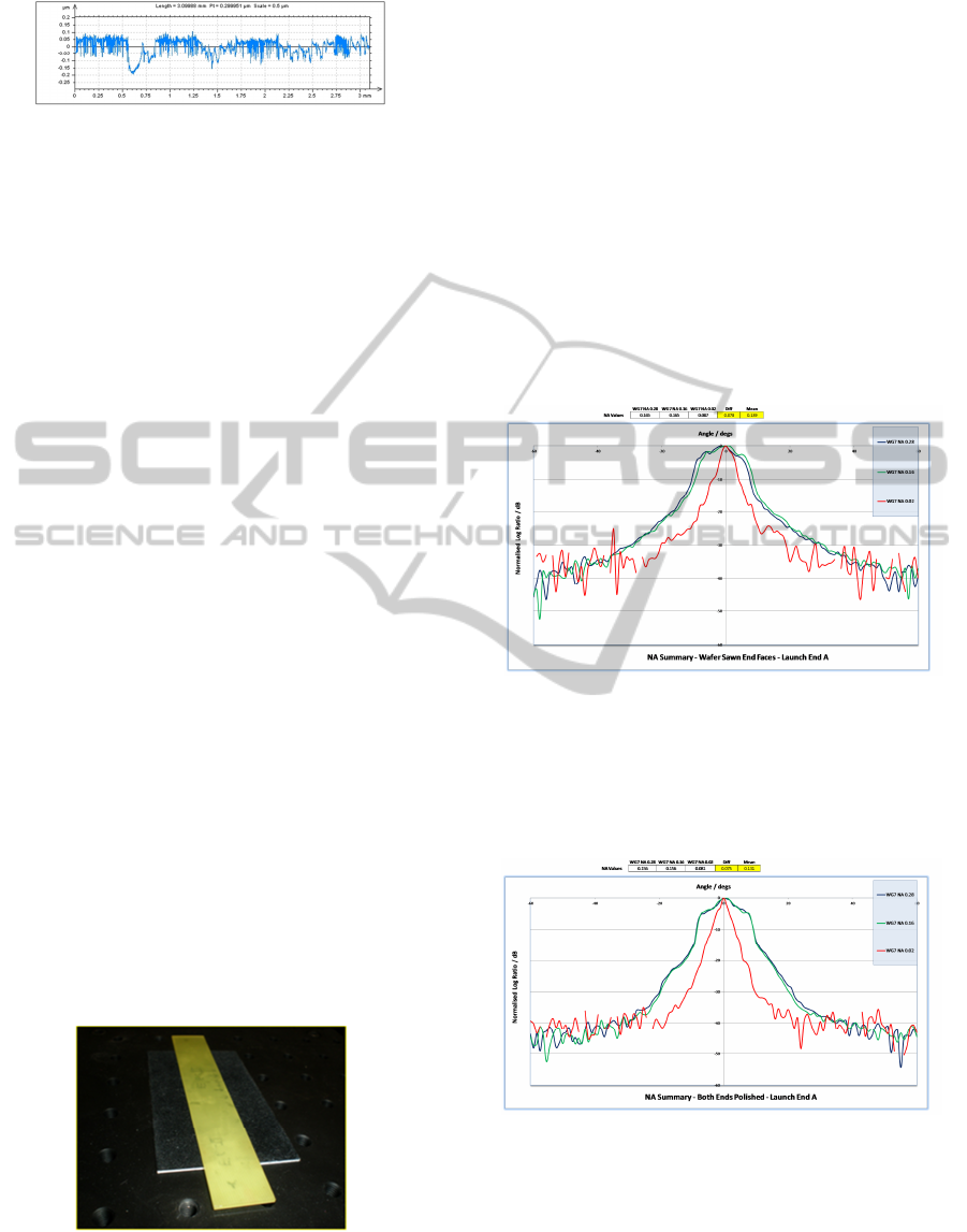
Figure 3: Typical surface roughness scan using the Talysurf
PGI 1000 made on one of the polished ends of the sample.
4 FAR-FIELD MEASUREMENTS
OF TRANSMITTED POWER
Measurements were made on a sample group of 30
x 30 µm siloxane (Kai Su, 2005) waveguides, ∼ 125
mm in length on an FR4 board produced using pho-
tolithography. The group was measured with both
wafer sawn and polished end faces. Using the system
described in Section 2, the transmitted power P(θ)
was measured over an angular scan range of ±60
o
in
1
o
steps. At each angular measurement an average of
100 frames was taken to improve the signal-to-noise
ratio and average the speckle. The entire measure-
ment scan was repeated three times to monitor the
stability of the launch. The measured power was nor-
malised to the reference power and measured using
the pick-off detector on the launch board, DET1. The
camera CCD1 is only used to allow alignment and fo-
cussing of the launch spot onto the input surface of
the waveguide under test. The launch NA was ini-
tially varied to investigate the subsequent changes in
the scatter profile for the different surfaces using a
spot size of 20 µm. More comprehensive measure-
ments were then carried out on the sample waveguide
group with the launch condition set to 0.16 NA and
an under-filled spot of 20 µm in order to emulate typ-
ical integrated VCSEL sources. The NA was calcu-
lated using the sine of the half angle at which the far
field intensity dropped to 5% of the peak value (IEC
60793-1-43 Ed. 1.0, 2001-07).
Figure 4: Sample OPCB containing groups of planar silox-
ane waveguides.
5 LAUNCH NUMERICAL
APERTURE COMPARISON
Changes were made to the launch condition by in-
creasing the numerical aperture from between 0.02,
0.16 and 0.28 NA. Far-field scans were carried out
with the end surfaces wafer sawn and with the ends
optically polished. As expected, the profiles reveal a
change in the exit NA with respect to the set launch
condition NA as more modes are excited within the
waveguide. However, the increase in the exit NA is
minimal once the launch NA increases beyond 0.16 to
0.28. The greater scatter associated with wafer sawn
surfaces shows a slight increase for each of the calcu-
lated NAs.
Figure 5: Far-field intensity scans of selected waveguides.
The graph shows normalised signal against angle on sam-
ple with wafer sawn end faces with a launch at End A.
Also shown are the calculated numerical apertures of each
waveguide.
Figure 6: Far-field intensity scans of selected waveguides.
The graph shows normalised signal against angle on sample
with optically polished end faces with a launch at End A.
Also shown are the calculated numerical apertures of each
waveguide.
PHOTOPTICS2013-InternationalConferenceonPhotonics,OpticsandLaserTechnology
98

6 RESULTS
AND UNCERTAINTIES
Figures 7 and 8 show the far-field scans for the se-
lected group of waveguides with two different end-
face surface treatments (with launches at ends des-
ignated A and B). For comparison measurements
launched into end A are shown first. The greater scat-
ter associated with the rougher surface of the wafer
sawn end faces tends to obscure the asymmetry as-
sociated with the waveguides and their performance.
The asymmetry of the scans is likely to be due to
corresponding material asymmetries in the waveg-
uide cross-section ie: a non-uniform refractive index
profile across the waveguides and along their length.
When looking at the waveguide group as launched
from end B the plots compare well between the two
different surface conditions. They also compare with
the scan profiles when launched at end A, especially
with the polished end faces. However, there is a clear
difference for the waveguides number 5 and 6 where
the scans exhibit a profile suggesting the presence of
cladding modes. As the scan has not been mathemat-
ically corrected for any electrical field inversion they
must be due to the presence of irregularities or defects
affecting these particular waveguides.
Figure 7: Far-field intensity scans of waveguide group con-
taining 7 individual waveguides. Graph shows normalised
signal against angle on sample with wafer sawn and pol-
ished end faces with a launch at End A. Also shown are the
calculated numerical apertures of each waveguide.
7 FAR-FIELD DISCONTINUITIES
Further investigation of waveguides 5 and 6 showed
how the far-field intensity profile can also be bene-
ficial in revealing any manufacturing defects in the
Figure 8: Far-field intensity scans of waveguide group con-
taining 7 individual waveguides. Graph shows normalised
signal against angle on sample with wafer sawn and pol-
ished end faces with a launch at End B. Also shown are the
calculated numerical apertures of each waveguide.
waveguides. A defect was observed that lay between
the two waveguide tracks, caused during the pho-
tolithographic manufacturing process. This produced
subsequent discontinuities in the associated far-field
scans (See Fig. 9)
Far-Field
Discontinuity
Figure 9: Far-field intensity scans of selected waveguides
5 and 6 affected by identifiable defect along waveguide
length.
8 CONCLUSIONS
We have modified an existing system to investigate
the far-field scatter of planar optical waveguides with
respect to launch condition and end face quality. The
scans have revealed that the dynamic range increases
with polished faces (up to ∼4 dB), which is consis-
tent with the improvement in the total attenuation ob-
tained through polishing the end faces. For each scan
the exit numerical aperture of the waveguides with re-
spect to the launch condition has been calculated from
the far-field scan. Polishing has been shown to give
Far-fieldScatterMeasurementsofPlanarOpticalWaveguidesusingaVariableLaunchSystem
99

no advantage in terms of NA which only increases
slightly when the board ends are polished from ∼0.03
to ∼0.09 NA. An important feature of the work has
been the ability to make use of the scanning process
to detect board defects that can affect the performance
of the waveguides. Discontinuities in the far-field pro-
file relate to identifiable board defects or inclusions
and the method has the potential to provide a rigorous
technique to assess the quality of waveguide manu-
facture. Polishing appears to accentuate any waveg-
uide inhomogeneity with the increased scatter due to
the rougher wafer sawn surfaces masking any waveg-
uide irregularities. There is evidence in the scans that
suggests the waveguide performance is not always bi-
directional. It is intended to use this set up to do
a more systematic study of the transmission quality
of waveguides produced using different methods and
the relationship between launch conditions and the re-
ceive detectors deployed in working boards operating
within data storage systems under a range of environ-
mental conditions.
ACKNOWLEDGEMENTS
We would like to thank Dr. Nikos Bamiedakis, Dr.
Terry Clapp and Professor Richard Penty of Cen-
tre of Advanced Photonics and Electronics, Cam-
bridge, for providing the sample waveguides and Neil
Lockmuller of the Engineering Measurement Ser-
vices Group at NPL for providing surface metrology
support.
This work was supported by the Department for
Business Innovation and Skills at NPL.
REFERENCES
D. R. Selviah, F. A. Fernndez, I. Papakonstantinou, K.
Wang, H. Bagshiahi, A. C. Walker, A. McCarthy, H.
Suyal, D. A. Hutt, P. P. Conway, J. Chappell, S. S. Za-
kariyah and D. Milward ”Integrated optical and elec-
tronic interconnect printed circuit board manufactur-
ing”, Circuit World, vol. 34, pp. 21-26, 2008.
Bamiedakis, N. Hashim, A., Penty, R. V., White, I. H., ’Re-
generative polymeric bus architecture for board-level
optical interconnects’, Optics Express 11625, Vol 20,
No. 11, 21 May 2012.
Kai Su, Jon V. DeGroot, Jr., Ann W. Norris and Peter
Y. Lo., ’Siloxane Materials for Optical Applica-
tions’, Advanced Technologies and Venture Business,
Dow Corning Corporation, 2200 W. Salzburg Road,
Midland, MI, USA 48686. Proc. Of SPIE Vol. 6029
60291C-7, (2005).
Ferguson, R., ’Waveguides Need Characterization, Too’,
Photonics Spectra, February 2012, pp.58-60.
Ives, D., Ferguson, R. A., Harris, S., ’Development of a
variable launch attenuation and isolation measurement
system for optical waveguides’, Applied Optics, Vol.
50, No. 22, 1 August 2011, pp. 4268 - 4275.
R. A. Ferguson and S. Harris, ”Development of an opti-
cal system with controlled launch conditions for the
characterisation of polymer optical fibre (POF)”, Op-
tical Fibre Measurement Conference Digest, 15 Octo-
ber 2007.
Leach, R. Measurement Good Practice Guide Number
37 - The Measurement ofSurface Texture using Sty-
lus Instruments, National Physical Laboratory, Crown
Copyright 2001, ISSN 1368-6550, July 2001.
IEC 60793-1-43 Optical fibres - Part 1-43: Measurement
methods and test procedures - Numerical aperture,
Publication date 26-07-2001.
PHOTOPTICS2013-InternationalConferenceonPhotonics,OpticsandLaserTechnology
100
