
A Buffer Cache Scheme Considering Both DRAM/PRAM Hybrid
Main Memory and Flash Memory Storages
Soohyun Yang and Yeonseung Ryu
Department of Computer Engineering, Myongji University, Yongin, Korea
Keywords: Hybrid Main Memory, PRAM, Flash Memory, Buffer Cache, Page Replacement.
Abstract: As the power dissipation has become one of the critical design challenges in a mobile environment, non-
volatile memories such as PRAM and flash memory will be widely used in the next generation mobile
computers. In this paper, we proposed an efficient buffer cache scheme considering the write limitation of
PRAM for hybrid main memory as well as the erase-before-write limitation of flash memory for storage
device. The goal of proposed scheme is to minimize the number of write operations on PRAM as well as the
number of erase operations on flash memory. We showed through trace-driven simulation that proposed
scheme outperforms legacy buffer cache schemes.
1 INTRODUCTION
Most modern operating systems (OS) usually
employ a buffer cache mechanism to enhance the
I/O performance that is limited by slow secondary
storage. When OS receives a read/write request from
an application, file system in OS copies the data
from storage to the buffer cache in the main memory
and serves the next operations from the faster main
memory. For the past decades, buffer cache schemes
have been implemented for DRAM-based main
memory and hard disk based secondary storage.
However, some recent studies have shown that
DRAM-based main memory spends a significant
portion of the total system power (Barroso and
Holzle, 2007). This is a serious problem with
battery-powered mobile computers such as smart
phones and tablet PCs. Fortunately, low-power non-
volatile memories such as PRAM (Phase change
RAM) and MRAM (Magnetic RAM) have been
developed. Among these non-volatile memories,
PRAM is rapidly becoming promising candidates for
large scale main memory because of their high
density and low power consumption. In order to
tackle the energy dissipation in DRAM-based main
memory, some recent studies introduced PRAM-
based main memory organization (Qureshi et al.,
2009) and DRAM/PRAM hybrid main memory
organization (Park et al., 2011). Though PRAM has
attractive features, the write access latency of
PRAM is not comparable to that of DRAM. Also,
PRAM has a worn-out problem caused by limited
write endurance. Since the write operations on
PRAM significantly affect the performance of
system, it should be carefully handled.
In most mobile computers, NAND flash memory
based storages have been commonly adopted
because flash memory is faster and consumes less
power than hard disks. However, flash memory
cannot be written over existing data unless erased in
advance and erase operation is much slower than
write operation. Further, the number of times an
erasure unit can be erased is limited. In order to
solve such problems, OS usually employs a software
layer called flash translation layer (FTL). An FTL
receives read and write requests from the file system
and maps a logical address to a physical address in
the NAND flash (Ryu, 2010).
In this paper, we study a buffer cache scheme for
future mobile computers which support
DRAM/PRAM hybrid main memory and flash
memory storages. Figure 1 illustrates the system
configuration considered in this paper. The goal of
proposed buffer cache scheme is to reduce both the
number of write operations on PRAM and the
number of erase operations on flash memory. We
show that the proposed scheme outperforms other
legacy schemes.
The rest of this paper is organized as follows. In
Section 2, we describe the characteristics of flash
memory and PRAM, and also describe the software
76
Yang S. and Ryu Y..
A Buffer Cache Scheme Considering Both DRAM/PRAM Hybrid Main Memory and Flash Memory Storages.
DOI: 10.5220/0004337200760079
In Proceedings of the 3rd International Conference on Pervasive Embedded Computing and Communication Systems (PECCS-2013), pages 76-79
ISBN: 978-989-8565-43-3
Copyright
c
2013 SCITEPRESS (Science and Technology Publications, Lda.)
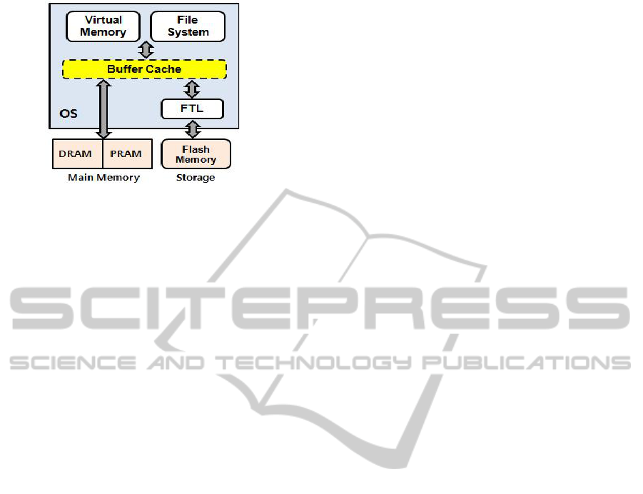
Figure 1: System configuration.
technologies, particularly FTL and buffer cache, for
these non-volatile memories. In Section 3, we
present a novel buffer cache scheme called HAC.
Section 4 presents the experimental results. Finally,
Section 5 concludes the paper.
2 BACKGROUND
2.1 Software for NAND Flash Memory
A NAND flash memory is organized in terms of
blocks, where each block is of a fixed number of
pages. A block is the smallest unit of erase
operation, while reads and writes are handled by
pages. Flash memory cannot be written over existing
data unless erased in advance. The number of times
an erasure unit can be erased is limited. The erase
operation can only be performed on a full block and
is slow that usually decreases system performance.
In order to solve erase-before-write problem, a kind
of device driver called FTL is usually implemented
in OS. The FTL performs the physical-to-logical
address translation to reduce the number of erase
operations. Most address translation schemes use a
log block mechanism for storing updates.
A log block scheme, called block associative
sector translation (BAST), was proposed by (Kim et
al., 2002). In the BAST scheme, flash memory
blocks are divided into data blocks and log blocks.
Data blocks represent the ordinary storage space and
log blocks are used for storing updates. When an
update request arrives, the FTL writes the new data
temporarily in the log block, thereby invalidating the
corresponding data in the data block. In BAST,
whenever the free log blocks are exhausted, in order
to reclaim the log block and the corresponding data
block, the valid data from the log block and the
corresponding data block should be copied into an
empty data block. This is called a merge operation.
After the merge operation, two erase operations need
to be performed in order to empty the log block and
the old data block. When the data block is updated
sequentially starting from the first page to the last
page, the FTL can apply a simple switch merge,
which requires only one erase operation and no copy
operations.
Further, there have been studies on buffer caches
schemes considering flash memory storages. A
page-level scheme called clean first least recently
used (CFLRU) was proposed by (Park et al., 2006).
CFLRU maintains a page list by LRU order and
divides the page list into two regions, namely the
working region and clean-first region. In order to
reduce the write cost, CFLRU first evicts clean
pages in the clean-first region by the LRU order, and
if there are no clean pages in the clean-first region, it
evicts dirty pages by their LRU order. CFLRU can
reduce the number of write and erase operations by
delaying the flush of dirty pages in the page cache.
Also, a block-level buffer cache scheme called
block padding LRU (BPLRU) was proposed, which
considers the block merge cost in the log block FTL
schemes (Kim and Ahn, 2008). BPLRU maintains a
LRU list based on the flash memory block.
Whenever a page in the buffer cache is referenced,
all pages in the same block are moved to the MRU
position. When buffer cache is full, BPLRU scheme
evicts all the pages of a victim block but it simply
selects the victim block at the LRU position. In
addition, it writes a whole block into a log block by
the in-place scheme using the page padding
technique. In page padding procedure, BPLRU reads
some pages that are not in the victim block, and
writes all pages in the block sequentially. The page
padding may perform unnecessary reads and writes,
but it is effective because it can change an expensive
full merge to an efficient switch merge. In BPLRU,
all log blocks can be merged by the switch merge,
which results in decreasing the number erase
operations.
2.2 Software for PRAM
A PRAM cell uses a special material, called phase
change material, to represent a bit. PRAM density is
expected to be much greater than that of DRAM
(about four times). Further, PRAM has negligible
leakage energy regardless of the size of the memory.
Though PRAM has attractive features, the write
access latency of PRAM is not comparable to that of
DRAM. Also, PRAM has a worn-out problem
caused by limited write endurance. Since the write
operations on PRAM significantly affect the
ABufferCacheSchemeConsideringBothDRAM/PRAMHybridMainMemoryandFlashMemoryStorages
77

performance of system, it should be carefully
handled.
For the DRAM/PRAM hybrid main memory, a
migration-based buffer cache scheme (we call it
MIG scheme) was proposed (Seok et al., 2012).
MIG maintains a page list by LRU order and evicts a
page from LRU position. In order to reduce the
writes on PRAM, MIG predicts the page access
pattern and migrates pages to DRAM or PRAM
according to the access pattern. MIG dynamically
moves the write-bound pages from PRAM to
DRAM, and moves the read-bound pages from
DRAM to PRAM. For prediction of the access
pattern, MIG calculates the weighting values of each
page at every request and maintains 4 types of
monitoring queues. MIG shows good performance
when the access pattern is highly skewed like
financial workload. Though MIG reduces the
number of write operations on PRAM, it does not
consider flash memory storages.
3 HYBRID MEMORY AWARE
CACHING
We propose a novel buffer cache scheme called
HAC (Hybrid memory Aware Caching). The
proposed HAC maintains a LRU list based on the
block of flash memory like Figure 2. The LRU list is
composed of block headers, each of which manages
its own pages loaded from flash memory.
When a page p of block b in the flash memory is
first referenced, the HAC allocates a new buffer and
stores page p in the allocated buffer. If the block
header for block b does not exist, the HAC allocates
a new block header and places it at the MRU
position of the LRU list. Then, the HAC attaches the
buffer of page p to the header of block b. Whenever
a page in the buffer cache is referenced, all pages in
the same block are moved to the MRU position.
We assume that the main memory is divided into
DRAM and PRAM by a memory address (Seok et
al., 2012). The memory which has the low memory
address is DRAM and the high section is allocated to
PRAM. When HAC allocates a new buffer, it tries to
allocate it from the low section. Further, the HAC
maintains the memory type (i.e., DRAM or PRAM)
of each block and tries to allocate buffers of the
same memory type to the block. When allocating a
DRAM buffer but there is no free DRAM buffer, the
HAC finds a clean (i.e., not modified) DRAM buffer
from the search region of the LRU list and makes it
free.
Figure 2: LRU list in HAC.
The HAC proposes an early deallocation technique
which frees clean DRAM buffers early even though
free buffers are still available in the system. Because
there could be a lot of used buffers that will not be
accessed soon in large-scale main memory, we can
free them early with little impact on the cache
performance. The HAC searches clean blocks which
use only DRAM buffers from the search region
periodically or whenever the number of free DRAM
buffers falls down below a threshold. Then, it frees
them. This technique can decrease the number of
writes on PRAM because the HAC can secure free
DRAM buffers for new allocations.
In order to further reduce the number of write
operations on PRAM, when a clean page in the
PRAM is referenced by a write operation, the HAC
allocates a DRAM buffer and writes requested data
to the DRAM buffer. Then it deallocates the PRAM
buffer. If there is no free DRAM buffer, the HAC
frees a clean DRAM buffer from the search region
and uses it for storing the requested write data.
If all buffers are used up, the HAC selects a
victim block from the search region. In order to
reduce the number of erase operations on flash
memory, the HAC tries to find a clean block and
simply frees all pages in it. If there is no clean block
in the search region, the HAC selects a victim block
at the LRU position of the block list, performs the
page padding technique, and flushes all pages of the
victim block.
4 EXPERIMENT
In order to evaluate the proposed scheme, we have
developed a trace-driven simulator. For the
workload for mobile computers, we extracted disk
I/O traces from notebook PC running several
applications for a week. The total I/O count is
706,833 and read/write ratio is about 55:45.
As shown in Figure 3 (a), the cache hit ratio is
very similar for all schemes. Figure 3 (b) shows that
the HAC outperforms other schemes in terms of the
PECCS2013-InternationalConferenceonPervasiveandEmbeddedComputingandCommunicationSystems
78

write counts on PRAM. The HAC reduces write
counts by roughly 13% on average and up to 26%.
In Figure 3 (c), the HAC can dramatically reduce the
erase counts on flash memory as BPLRU does.
Further, the HAC outperforms BPLRU because it
considers clean blocks to avoid erase operation
during replacement procedure.
(a) Cache hit ratio.
(b) Write counts on PRAM.
(c) Erase counts on Flash.
Figure 3: Performance evaluation result.
5 CONCLUSIONS
It is highly expected that low-power non-volatile
memories such as PRAM and flash memory will
become popular in mobile computers. The proposed
buffer cache scheme supports DRAM/PRAM hybrid
main memory and flash memory storages. We
showed through trace-driven simulation that
proposed scheme outperforms legacy buffer cache
schemes.
ACKNOWLEDGEMENTS
This research was supported by Basic Science
Research Program through the National Research
Foundation of Korea (NRF) funded by the Ministry
of Education, Science and Technology(2010-
0021897).
REFERENCES
Barroso, L., Holzle, U., 2007. The Case for Energy-
proportional Computing. Computer, Vol.40, No.12.
Qureshi, M., Srinivasan, V., Rivers, J., 2009. Scalable
High Performance Main Memory System Using
Phase-Change Memory Technology. In Proceedings
of International Symposium on Computer
Architecture.
Park, H., Yoo, S., Lee, S., 2011. Power Management of
Hybrid DRAM/PRAM-based Main Memory. In
Proceedings of Design Automation Conference.
Kim, J., Noh, S., Min, S., Cho, Y., 2002. A Space-
Efficient Flash Translation Layer for Compactflash
Systems. IEEE Transactions on Consumer Electronics,
Vol. 48, No. 2, pp. 366-375.
Ryu, Y., 2010. SAT: Switchable Address Translation for
Flash Memory Storages. In Proceedings of IEEE
Computer Software and Applications Conference.
Park, S., Jung, D., Kang, J., Kim, J., Lee. J., 2006. CFLRU:
A Replacement Algorithm for Flash Memory. In
Proceedings of International Conference on
Compilers, Architecture and Synthesis for Embedded
Systems.
Kim, H., Ahn, S., 2008. BPLRU: A Buffer Management
Scheme for Improving Random Writes in Flash
Storage. In Proceedings of the 6th USENIX
Conference on File and Storage Technologies.
Seok, H., Park, Y., Park, K., Park, K., 2012. Efficient Page
Caching Algorithm with Prediction and Migration for
a Hybrid Main Memory. Applied Computing Review,
Vol. 11, No. 4.
ABufferCacheSchemeConsideringBothDRAM/PRAMHybridMainMemoryandFlashMemoryStorages
79
