
Simulation of Self Organized Electron Beams
in Vacuum Microdiodes
Marjan Ilkov
1
, Andreas Pedersen
2
, Andrei Manolescu
1
and Ágúst Valfells
1
1
School of Science and Engineering, Reykjavík University, Menntavegi 1, Reykjavík, Iceland
2
Science Institute, University of Iceland, Dunhaga 3, Reykjavík, Iceland
Keywords: Vacuum Microelectronics, Molecular Dynamics, Electron Beam, Space-charge Limited Flow, Terahertz.
Abstract: Simulation of vacuum micro-diodes can be done quite effectively using molecular dynamics methods. This
results in much higher fidelity simulations than can be obtained using the particle-in-cell method (PIC),
which is most common for plasma and particle beam simulations. In particular, this method is superior to
the PIC method when treating systems where collisional effects are important. In this paper we present some
results concerning electron beam structure in a vacuum micro-diode obtained using a molecular dynamics
code developed at Reykjavík University.
1 INTRODUCTION
Vacuum electronics devices have been in continuous
use for over a hundred years although their
applications have varied (Barker et al, 2002);
(Eichmeier and Thumm, 2008). As the name implies
they are based on transporting electrons, or other
charged particles, through a vacuum, often guided
by electric and magnetic fields. Prior to the advent
of the solid state transistor vacuum tubes were
ubiquitous in electronics, but since then their use has
become more specialized. In particular, vacuum
electronic devices have been used for high power
and high frequency applications where their superior
performance characteristics have seen them keep the
solid-state devices at bay.
The main drawback of vacuum electronic
devices has been the complexity of their
construction and the need to maintain a good
vacuum for them to function properly. However,
power efficiency and robustness are examples of
their advantages. With the advent of modern
fabrication techniques it is now possible to
manufacture three dimensional microstructures in an
inexpensive and reliable manner. An advantage of
operating vacuum devices at the micro-scale is that
the mean free path of electrons is of the same order
as the characteristic dimension of the device itself
even at atmospheric pressure. Thus the “vacuum”
characteristics of the device are due to the small size
rather than the low pressure. As a result of these
developments the possibility arises for vacuum
electronics devices to become an attractive option in
many applications where they had been too costly
before.
When modelling vacuum devices at this small
scale it is important to take into account several
physical effects that can, to a large degree be
ignored in macro-scale devices, e.g. scattering and
surface inhomogeneity. An important advantage is
that the number of free electrons in such small
systems is typically on the order of 10
2
to 10
4
and as
a result it is practical to use a molecular dynamics
method where the repulsive Coulomb interaction
between every single free electron is taken into
account. This means that discrete effects can be
modelled with high fidelity –something that is not
possible to the same extent with the particle-in-cell
(PIC) methods that prevail in the plasma physics and
vacuum electronics community.
Our previous work on a single emitter has shown
that in the case of photoemission, when many
electrons are released at the same time from a
nanometric cathode, one may expect an oscillatory
current through the device (Pedersen, 2010). Similar
results have been obtained (de Lara et al., 2006), but
with emitters larger than few millimeters. These
oscillations are a result of the repulsive Coulomb
forces between the electrons in the micro diode. A
bunch of electrons just released from the cathode
will be accelerated by the electric field across the
224
Ilkov M., Pedersen A., Manolescu A. and Valfells Á..
Simulation of Self Organized Electron Beams in Vacuum Microdiodes.
DOI: 10.5220/0004595502240228
In Proceedings of the 3rd International Conference on Simulation and Modeling Methodologies, Technologies and Applications (SIMULTECH-2013),
pages 224-228
ISBN: 978-989-8565-69-3
Copyright
c
2013 SCITEPRESS (Science and Technology Publications, Lda.)

diode, but will also create an opposite electric field
that may block the release of further electrons from
the cathode temporarily. This novel beam bunching
mechanism may be useful as a tunable oscillator
operating in the THz domain. The frequency of the
current at the anode is determined by the vacuum
field and by the size of the emitter (Jonsson, 2013).
These unexpected results have motivated us to
expand the study to investigate the effects of having
an emitter area which is non-continuous, e.g. two
circular emitters separated by a given distance or an
arrangement of square emitters on the cathode. This
is a preliminary step in studying several diodes
working in parallel, which is required to increase the
output power of a corresponding device. In this
paper a brief outline on how the molecular dynamics
approach has been used to model vacuum micro-
diodes will be given, as well as preliminary results
regarding beam structure that emerges in the diode
due to nonlinear Coulomb interaction between the
particles in the electron beam released by two
cathode areas. We will discuss both longitudinal (or
temporal) and transverse structure in the beam due
to these types of arrangements.
2 SIMULATION APPROACH
The system under consideration consists of a parallel
plate vacuum diode. The cathode is grounded, and
the anode is at a potential, . The spacing between
the anode and cathode is D. In the absence of any
electrons in the gap between the cathode and anode
the electric field is uniform and perpendicular to the
electrodes and given by E
0
= /D. This is referred to
as the vacuum field. Electrons originate at the
cathode and are accelerated in the gap by the electric
field. Once electrons are present in the gap they
bring a new component of the electric field into
existence due to their own charge (the space-
charge). In the event that the number of electrons in
the gap becomes large enough the space-charge field
can become a dominant factor in the beam
dynamics, even to such an extent that it will inhibit
further electrons from being emitted. This is known
as the space-charge limited regime, and when
operated under this condition the beam dynamics is
highly nonlinear. In our model we assume that
electrons are emitted from a cold cathode via
photoemission, with negligible initial velocity.
In the simulation each time step is broken down
into three sub-steps: Particle emission, particle
advancement and absorption. A brief description
will be given here, but a more complete description
may be found in (Jonsson 2013).
2.1 Particle Emission
At the beginning of each time step a random point
on the emitter area is selected. If the electric field at
that point is favourable in terms of pushing an
electron into the diode gap an electron will be placed
slightly above that point. If the field is unfavourable
a failure of placement will be registered. While
keeping time constant, this process is repeated,
taking into account the electric field stemming from
those electrons that have been placed in the system
already. The iteration of this process is continued
until 100 consecutive placement failures have been
registered, at which time it is deemed that space-
charge limited emission has been reached.
The emission can also be source limited, in
which case the number of electrons per time step is
limited to a predefined number, but that regime will
not be discussed further in this paper.
2.2 Particle Advancement
Once the space-charge limit has been reached, the
force acting on each individual free electron in the
system is calculated, taking into account both the
external electric field and the Coulomb force from
every single other free electron in the diode gap.
Subsequently a velocity-Verlet method is used to
calculate each electrons position at the end of the
time step.
2.3 Particle Absorption
After calculating the final position of all the free
electrons at the end of the time step, we determine
which electrons have passed beyond the boundary of
the diode and will be absorbed. The number of
electrons absorbed at the anode per time step is used
as a basis for calculating the time dependent current
in the diode, which is obtained using a smoothed
average of the absorption rate. Additionally the point
of absorption is also registered.
3 RESULTS
In our simulations we consider circular (disk) or
square emitters on the cathode. The spacing between
the cathode and anode is 500nm, and the electric
potential is 2V. The time step used in the simulation
is 0.25fs.
SimulationofSelfOrganizedElectronBeamsinVacuumMicrodiodes
225
3.1 Temporal Structure
We consider two circular emitters of radius 150 nm.
We want to observe whether and how the Coulomb
oscillations of the current are established in a device
with two emitters working in parallel. We assume
that in a realistic setup the two emitters may not be
synchronized. Therefore we consider in the
simulations a certain relative time delay, and the
current begins to be drawn from one emitter before
the other one. We set the time delay to one fourth of
the period of the space charge induced oscillation,
i.e. the current from the two circular emitters is
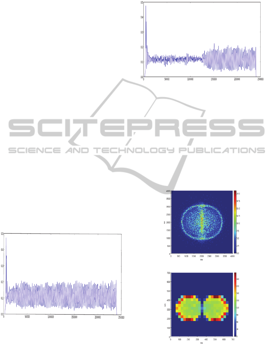
initially 90° out of phase. Figures 1 and 2 show the
temporal profile of the current at the anode for two
different values of the spacing between the emitting
disks. In Fig. 1 the distance between the centers of
the disks is 305 nm, i.e. the disks are almost
touching. In this case the onset of regular current
oscillations starts after about 10 000 time steps.
After this time the emission from the two disks on
the cathode becomes synchronized and the current is
qualitatively similar to that corresponding to a single
disk. In Fig. 2 the distance between the centers of
the disks is increased to 340 nm. In this case we see
a much longer transient phase of fairly weak and
chaotic oscillations. But, as time goes by the current
from the two disks becomes synchronized and the
amplitude of the oscillation grows to the same level
as in Fig. 1. We have observed that the
synchronization occurs even for larger spacing
between the emitters, but only after a longer
transient time.
Figure 1: Current at the absorber vs. time steps for two
identical circular emitters, each one with radius of 150nm
The distance between the centers of the disks is 305 nm,
i.e. the disks are almost touching. . The current is given
arbitrary units and one time step is 2.510
-16
s.
Figure 2: Current at the absorber vs. time steps for two
identical circles (disks) with radius of 150 nm. The
distance between the centers of the disks is 305 nm, i.e.
the disks are almost touching. The current is given
arbitrary units and one time step is 2.510
-16
s.
3.2 Transverse Structure
We are interested in time-integrated charge
absorption at the anode and its distribution
perpendicular to the axis of beam propagation. This
is the equivalent of what would be measured using
the well-known experimental method of inserting a
fluorescent screen into the path of an electron beam.
Thus it is a useful method of comparison.
Figure 3: Two identical circles with radius of150nm with
centers separated by 305nm. Here the delay of 90
o
was
introduced in the emission start between the two circular
emitters.
SIMULTECH2013-3rdInternationalConferenceonSimulationandModelingMethodologies,Technologiesand
Applications
226
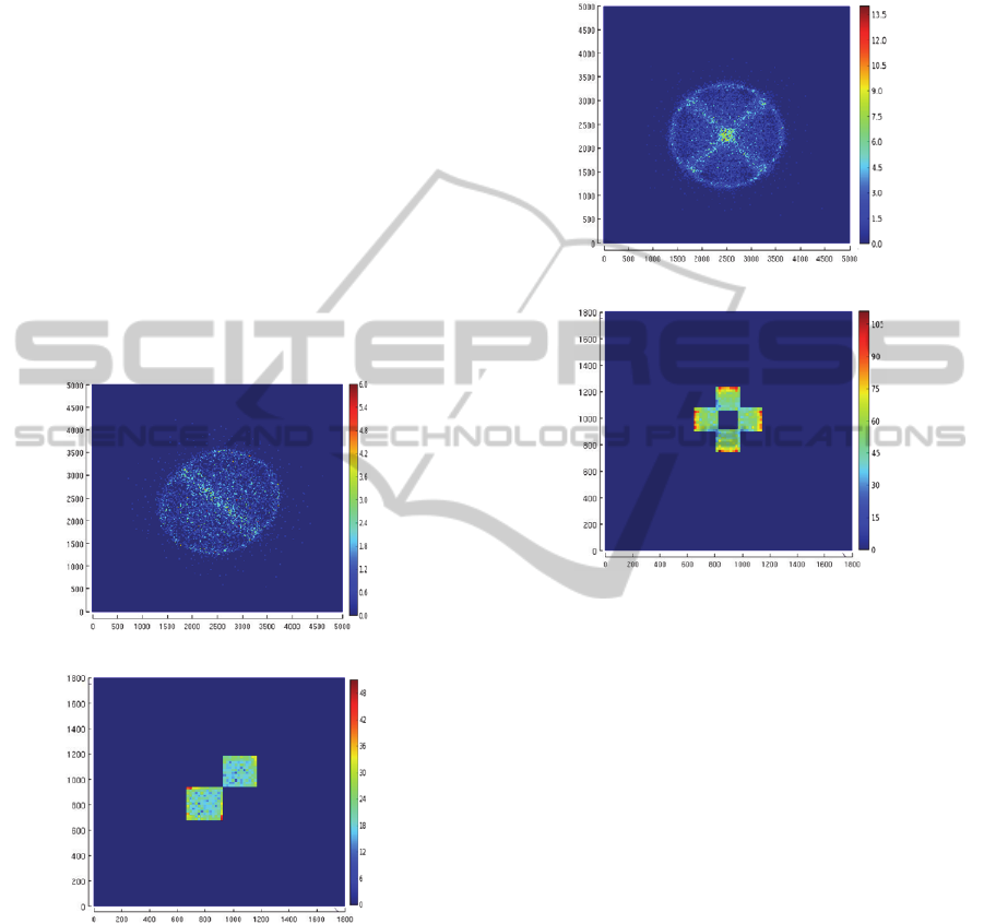
We begin by looking at the same configuration
as was used for investigation of the temporal
structure, namely two emitting disks of radius
150nm with their centers separated by 340nm.
Figure 3 shows the resulting pattern for absorption at
the anode as well as that for emission at the cathode.
We note that on the cathode, the current density is
highest along the outer edges. This is in agreement
with previous studies for two-dimensional space
charge limited emission (Ragan-Kelley, 2009). We
also note that at the anode, the beam takes on a
circular cross section with a prominent halo. This is
in agreement with the general characteristics of
space charge dominated electron beams (Reiser,
2008). An interesting aspect is the bright line that
dissects the circle on the upper part of Figure 3
(corresponding to the anode). This is along the line
of the system and is due to interference of the
current from the two emitters.
Figure 4: Two identical squares with side of 250nm each
touching at the corners.
Next we conduct a similar investigation with
slightly different configurations. First, we have two
square emitters of side length 250nm touching at the
corners, as depicted in Figure 4. Second a matrix of
four identical squares with a side length of 250nm,
touching at the corners as depicted in Figure 5. Once
again we see that the beam pattern evolves into a
circular form with a prominent halo. At the cathode
the current is most intense at the outer edges of the
emitter area. As before, we see that this is in
character with expected beam behaviour. Similarly
we also find that the charge density is greater along
the lines of symmetry in the system.
Figure 5: Four identical squares with side of 250nm each
touching at the corners.
4 CONCLUSIONS
We have developed a code for conducting high
fidelity molecular dynamics simulations of vacuum
microsystems with full representation of Coulomb
forces. With this code we have been able to observe
emergence of both temporal and spatial structure in
the beam due to space charge forces. This holds
some promise for the development of tuneable THz
radiators and for the design of electron beamlets
with a specified microstructure.
ACKNOWLEDGEMENTS
This research has been funded by the Icelandic
Research Fund (Rannis), project grant number
120009021.
SimulationofSelfOrganizedElectronBeamsinVacuumMicrodiodes
227

REFERENCES
Barker, R. J, Booske, J. H, Luhmann, N. C. Nusinovich,
G. S., 2002.Modern microwave and millimeter-wave
power electronics,IEEE Press.
De Lara, J., Pérez, F., Alfonseca, M., Galán, L., Montero,
I., Román, E., Raboso Garcia-baquero, D., 2006,
Multipactor Prediction for On-Board Spacecraft RF
Equipment with the MEST Software, IEEE
Transactions on Plasma Science
Eichmeier, J. A., Thumm, M., 2008, Vacuum electronics,
components and devices, Springer.
Jonsson, P., Ilkov, M., Manolescu, A., Pedersen, A., and
Valfells, A., 2013., Physics of Plasmas 20, 023107.
Pedersen, A., Manolescu, A., Valfells, A.,2010. Phys. Rev.
Lett. 104, 175002.
Ragan-Kelley, B, Verboncoeur, J, Feng, Y., 2009.Physics
of Plasmas 16, 103102.
Reiser, M, 2008. Theory and design of charged particle
beams, Wiley, 2
nd
edition.
SIMULTECH2013-3rdInternationalConferenceonSimulationandModelingMethodologies,Technologiesand
Applications
228
