
An Automatic Vision System using Optical Scanning Mechanism
with Near-infrared Optics for Solar Cell Wafer
Gyung-bum Kim
Dept. of Aeronatical & Mechanical Eng, Korea National University of Transportaion, Chungju, South Korea
Keywords: Optical Scanning Mechanism, Solar Cell Wafer, Surface Inspection System, Near-infrared Optics.
Abstract: In this paper, an automatic vision system based on optical scanning mechanism is developed for solar cell
wafer. It consists of optical scanning mechanism with near-infrared(NIR) camera optics, machinery and
control system, algorithm of defect detection and software. Optical scanning mechanism is composed of
geometrical camera optics and structured hybrid illumination system(SHIS). It is used to inspection of
surface defects. Also, NIR camera optics is used for inspection of defects inside solar cell wafer. It is shown
that the automatic inspection system give satisfactory performance for micro defects in solar cell wafer.
1 INTRODUCTION
Solar energy using solar cell wafer is considered as
renewable green energy. The silicon wafer is an
inevitable part in solar cell. Its thickness has been
slim so far due to competition of cost. It is because
the cost of silicon wafer manufacturing is involved
more than 60% in solar cell manufacturing. A lot of
defects such as topology defects, surface defects and
internal micro defects, are generated in silicon wafer
manufacturing. They highly result from slimmer
thickness of silicon wafer. They result in high
manufacturing cost and lack of efficiency. Therefore,
the automatic inspection of defects in solar cell
wafer is urgently required.(Li, 2011)
In this paper, an automatic inspection system is
developed for solar cell wafer. It is composed of
optical scanning mechanism, NIR camera optics,
machinery and control system, defect detection
algorithm and software.
2 OPTICAL SCANNING
MECHANISM
2.1 Geometric Camera Optics
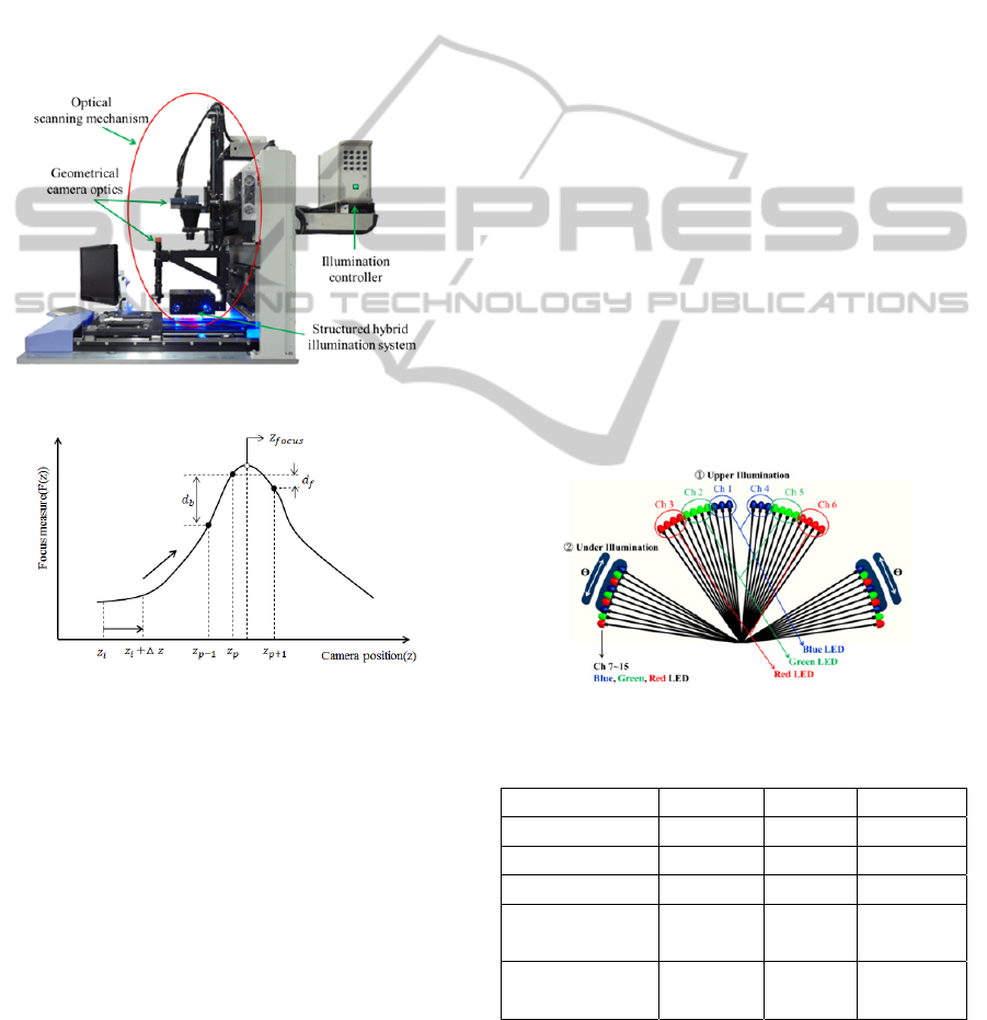
The optical scanning mechanism in Figure 1 is
designed for solar cell wafer. It is composed of
geometric camera optics, structured hybrid
illumination system(SHIS). High-speed machine
vision must be applied to manufacturing process of
solar cell wafer due to fast production line.(Golnabi,
2007) To implement the fast inspection, TDI(time
delay & integration) line scan camera is used. It has
high sensitivity and is used as inspection camera in
geometric camera optics. Also, an area camera with
high resolution is used as monitoring. The detail
specifications of optical scanning mechanism is in
Table 1.
Table 1: Specification of geometrical camera optics.
Lists Specification
Line scan
camera
Resolution: 8192×32TDI
Pixel size: 7×7 ㎛
Line rate: up to 34kHz
Area camera
Image sensor: SONY CCD
Resolution: 1280×1024
Frame rate: 15fp
Lens
Macro-
symmar
5.6/102
Focal length: 120mm
Mag.: 0.38 ~ 0.63x
Max aperture: F5.9
Zoom
70XL
Zoom range: 7:1
Mag.: 0.75 ~5.25x
Work distance: 89mm
Frame grabber
SOL 2M EV CLF
Data acquisition: Camera link
Image library MIL 9.0
The best focused position of camera can be found
27
Kim G..
An Automatic Vision System using Optical Scanning Mechanism with Near-infrared Optics for Solar Cell Wafer.
DOI: 10.5220/0004679200270030
In Proceedings of the 4th International Conference on Pervasive and Embedded Computing and Communication Systems (PECCS-2014), pages 27-30
ISBN: 978-989-758-000-0
Copyright
c
2014 SCITEPRESS (Science and Technology Publications, Lda.)
automatically. To solve this problem, the hill
climbing algorithm(Cho, 2006) is used as auto
focusing method. It determines the direction of the
lens and camera movement in order to search for the
maximum value of the focus measure in Figure 2.
Also, lens magnification can be automatically
adjusted. the length between solar cell wafer and
lens is 'a' and length between lens and camera sensor
is 'b', the lens formula is formed by Gaussian lens
principle. Here, focal length of lens is f. Once f, a
and b are changed, magnification M is varied. The
optical scanning mechanism can change lens
magnification through controlling the interval of 'b'.,
Figure 1: Optical scanning mechanism.
Figure 2: Distribution of focus measure for autofocusing.
2.2 Structured Hybrid Illumination
System
An illumination system is used to keep uniformly
good contrast between object and background in
machine vision. Illumination conditions for high-
quality and reliable images are very important,
because suitable illumination conditions result in the
extraction of useful features.(Sunil, 2006) There are
a lot of illumination methods exclusive of
illumination sources such as bright field, dark field,
dome light, oblique front light, directional front
light, diffusion front light, back light, co-axial light
and structured light etc..
In this paper, SHIS(Kim, 2012) are designed to
optionally use bright field, dark field, oblique front
light, directional front light and diffusion front light,
in accordance with inspection environment. SHIS
consists of upper illumination in Fig. 3 ① and under
illumination in Fig 3 ②. SHIS is symmetry structure
against optical axis. The upper illumination is
mainly the bright field method and can use
directional front light because illumination channels
are separately controlled. The channel 1 and 4 are
Blue LED, channel 2 and 5 are Green LED and
channel 3 and 6 are Red LED. The under
illumination is usually used for dark field method
and oblique front light. The channel 7~15 consist of
Blue-Green-Red LED in order. Each channel row is
separately controlled but it is symmetrically
controlled in the same time. Also, angle of under
illumination can be adjusted in a certain range θ.
Illumination source is LED. The advantages of LED
are high efficiency, uniformity of luminance, no
flicker, long lifetime and requirement of low current.
All illumination channels are directed to one point.
The used LED specifications are in Table 2.
Diffusion filter is utilized in order to uniform and get
a smooth image. SHIS makes an efficient
combination of upper and under illumination. When
all upper and under illumination are used, SHIS can
be used as diffusion front light.
Figure 3: Structured hybrid illumination system.
Table 2: Specification of LED.
List Blue Green Red
Forward Current 35mA 35mA 30mA
Forward voltage 3.2V 3.2V 2.1V
Wavelength 471nm 525nm 628nm
Operation
temperature
-30 ~ 85 -30 ~ 85 -30 ~ 85
Luminous
intensity
8200mcd 9600mcd 12000mcd
2.3 NIR Camera Optics
Infrared ray is used as heat source. Solar cell wafer
PECCS2014-InternationalConferenceonPervasiveandEmbeddedComputingandCommunicationSystems
28
can be damaged by its longtime incidence.
Accordingly, The infrared spectrum band that has a
little transmittance as well as weak heat source
needs to be selected for solar cell wafer. It is
regarded as the spectrum of near-infrared ray. In
case NIR is incident to solar cell wafer, full
reflectance ray is represented from surface. Also,
while the phenomenon of transmittance and
reflectance is represented in repetition by optical
scattering inside wafer, the ray of absorption, body
reflectance and transmittance resulting in solar cell
wafer is dispersed in all direction.(Choi, 2006)
Inspection of internal micro defect uses
transmission characteristic of NIR because it is not
inspected in general illumination like LED and
halogen. NIR camera optics is known as temperature
detection of object because it is mainly affected by
heat source. But, NIR camera optics is not detection
of heat source. NIR camera optics acquires
wavelength that is not transmitted by visible ray.
Solar cell wafer has a relatively high transmission
characteristics about wavelength of 1 micron level.
Using this principle, images of internal defects can
be acquired in NIR camera when NIR light is
incident to solar cell wafer by back light method.
NIR camera optics in Fig. 4 is designed for internal
micro defect inspection of solar cell wafer. Its detail
specifications are in Table 3.
Figure 4: NIR camera optics.
3 AUTOMATIC INSPECTION
SYSTEM
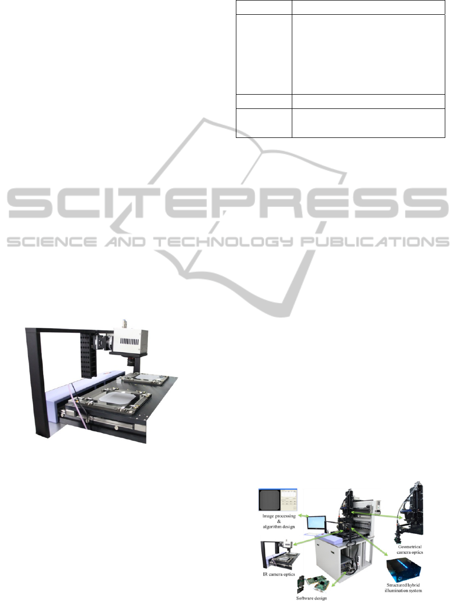
The automatic inspection system for solar cell wafer
is described in Figure 5. It consists of optical
scanning mechanism with NIR camera optics,
machinery and control system, algorithm of defect
detection and software.
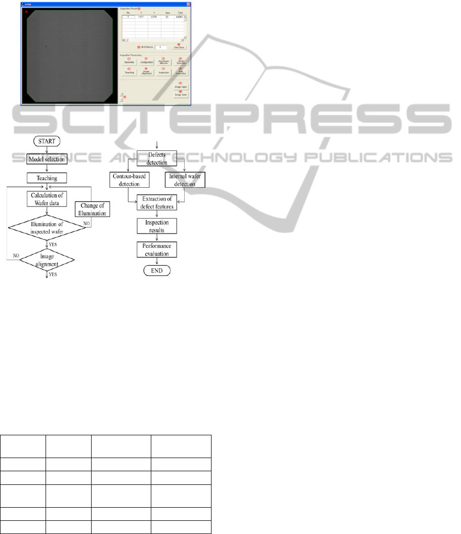
The inspection software is described in Figure 6,
and includes 15 software modules. They are as
follows; (1) Geometry: Translation and rotation of
Table 3: Specification of NIR camera optics.
Lists Specifications
NIR
camera
Array type: InGaAs
Spectral band: 900~1700nm
Pixels: 320×256 ㎛
Pixel operability: >99%
Frame rate: 100Hz, 12bit
Camera control: USB 2.0
Lens Compact VIS-NIR lens
Illumination
Infrared halogen light source: 1127nm
IR back light source: 850~940nm
inspected image (2) Configuration: confirmation and
modification and of inspected image information
from teaching reference image (3) Anisotropic
diffusion: Image filtering option (4) Model selection:
information save in specified region of reference
image (5) Teaching: Save of wafer information (6)
Image alignment: alignment of inspected image
based on reference image (7) Inspection: defect
detection of inspected wafer based on reference
image (8) Auto inspection: automatic execution of
detection and inspection process using Figure 7 (9)
Image open (10) Image save (11) Zoom in/out (12)
Inspection result: information of detection defect (13)
Number of defects.
Its inspection performance has been evaluated
for various defects such as pinhole, scratch, edge
defect, stain and sawmark, in terms of accuracy,
repeatability and undetected error rate. Inspected
wafers with no defect, pinhole, scratch, edge defect,
stain and sawmark, are prepared for the simulation
of real inspection. Their number is 50 sheets,
respectively. So, the total wafer number is 300. The
inspection results is shown in Table 4. The
developed algorithm results in 100% accuracy for
defects such as pinhole, stain and sawmark. It gives
excellent results. Also, its accuracy is 96% for edge
defect and 92% for edge defect. Its undetected error
rate is 4% and 8% for scratc and edge defect,
Figure 5: Automatic inspection system.
AnAutomaticVisionSystemusingOpticalScanningMechanismwithNear-infraredOpticsforSolarCellWafer
29
respectively. The developed algorithm gives 100%
detection repeatability. In case the inspected image,
relative to the reference image, two defects such as
edge defect and scratch can not be detected. This
result from non-uniformity of wafer edge and
internal wafer. As a result, the useful performance of
our algorithm is verified through detection
experiments using 5 types of defects.
Figure 6: The inspection software.
Figure 7: Flow chart of defect detection algorithm.
4 CONCLUSIONS
In this paper, an automatic vision inspection system
based on optical scanning mechanism with NIR
optics is developed for solar cell wafer. It consists of
optical scanning mechanism with NIR camera
optics, machinery and control system, algorithm of
Table 4: Results of performance evaluation.
Lists Accuracy Repeatability
Undetected
error rate
Pinhole 100% 100% -
Scratch 96% 100% 4%
Edge
defect
92% 100% 8%
Stain 100% 100% -
Sawmark 100% 100% -
defect detection and software. It is shown that the
developed inspection system gives useful and
excellent results in performance evaluation and is
applied to measurement and inspection processes
related with surface quality control as well as solar
cell manufacturing.
ACKNOWLEDGEMENTS
This research was supported by Basic Science
Research Program through the National Research
Foundation of Korea(NRF) funded by the Ministry
of Education, Science and Technology(2012001630)
REFERENCES
Li, W. C. and Tsai, D. M., 2011. Automatic Saw-mark
Detection in Multi-crystalline Solar Wafer Images,
Solar Energy Materials & Solar cells, DOI:
10.1016/j.solmat.2011.03.025.1.
Sunil, K. K., 2006. Lighting Design for Machine Vision
Application, Image & Vision Computing, Vol. 24, pp.
720-726.
Golnabi, H., Asadpour, A., 2007. Design and application
of industrial machine vision systems, Robotics and
Computer-Integrated Manufacturing, Vol. 23, pp. 630-
637.
Choi, M. Y., et al, 2006. Measurement of Defects and
Stress by Infrared Thermography, Journal of Korean
Society of Precision Engineers, Vol. 23, No. 10, pp.
30~35.
An, B. I. and Kim, G. B., 2012. Development of structured
hybrid illumination system and optimum illumination
condition selection for detection of surface defects on
silicon wafer in solar cell, Journal of the Korean
Society of Mechanical Engineers(A), Vol. 36, No. 5,
pp. 336~337.
Cho, H. S., 2006. Optomechatronics, Taylor & Francis.
Kim, G. B., 2010. A structured mechanism development
and experimental parameter selection of laser
scattering for the surface inspection of flat-panel
glasses, International Journal of Production Research,
Vol. 13, No.49, pp. 3911~3923.
Kim, G. B., Yeon, J. S., 2011. Development of laser
scattering system and inspection of micro defects in
crystalline silicon wafer of solar cell, Proceedings of
the 11th EUSPEN International Conference, pp.39-42.
PECCS2014-InternationalConferenceonPervasiveandEmbeddedComputingandCommunicationSystems
30
