
Directionality Control of Light-emitting Devices through Sub-micron
Dielectric Structures
Yoshikuni Hirano, Katsu Tanaka, Yasushi Motoyama, Nobuo Saito
and Hiroshi Kikuchiand Naoki Shimidzu
Science & Technology Research Laboratories, NHK (Japan Broadcasting Corporation),
1-10-11 Kinuta, Setagaya-ku, Tokyo, Japan
Keywords: Light-emitting Diodes, Directionality Control, Direct-view-Type Display.
Abstract: We have been investigating directional light control methods of light-emitting diodes (LEDs). We propose a
method that makes it possible to control a principal axis in field intensity through fine-structures on the
LEDs. We also describe the concept of this method and essential points for obtaining a sharply defined
principal axis. The effectiveness of the method was verified through differences in angular distributions by
using the finite-different time-domain method.
1 INTRODUCTION
Light emitting diodes (LEDs) are expected to be a
next generation light source and have been applied
to many lighting applications, such as general
lighting (Krames, 2007), visible-light
communication (McKendry, 2012), and displays
(Day, 2011) due to advances in high-brightness
technology. Because of the Lambertian pattern in the
spatial intensity distribution of an LED, the direct-
view-type display, which consists of as many fine
LED chips as the number of pixels, has wider
viewing angles (Sony corp., 2012).
The Lambertian pattern is not suitable for certain
applications, and the directionality control of LEDs
has been studied for mainly narrowing the angular
distribution. In an automotive lighting area, for
example, the sharper angular distribution will enable
the lighting of a restricted region and reduce
blinding glare from oncoming vehicles (Krames,
2007). In projection display systems, light use
efficiency is improved by increasing the incident
light flux from a light source to projection optics
(Fournier, 2008). In addition to the modifying
angular distribution of LEDs, new applications will
be possible if off-axis directionality control becomes
possible.
Projection optics for modifying the far-field
pattern of an LED is also important to downsize
projection display systems (Tu, 2009). Recently,
several directional light control methods have been
proposed for LEDs with photonic crystals
(McGroddy, 2008). For instance, the angular
distribution of the directional light at half intensity
near 66º from a 5-m aperture was demonstrated in
an experiment with a prototype of GaN-based LEDs
with photonic crystals (Lai, 2012). This result
indicates that increasing light emission in useful
directions eliminates the need for some optical
elements to concentrate the emission light from an
LED into projection optics. The directional light
control method enables a projector to be small, light
weight, and exhibit high definition. In addition, the
off-axis directionality control reduces the projection
optics and allows more compact projection systems.
However, more complex designed crystal lattice and
excessive lattice points are necessary to achieve
sharply defined off-axis directional light beam.
Off-axis directionality control allows high
picture quality technology for auto-stereoscopic
three-dimensional (3D) multi-view displays (Son,
2010). Several types of 3D displays produce 3D
images by using many directional lights using a
multi-projector, parallax barrier, and lens array. The
ideal 3D display requires a number of directional
lights across the entire viewing space. Therefore, a
high-density array of an off-axis directionality-
controlled light emitting device is useful for such 3D
displays. More recently, multi-directional backlight
technology has been proposed to provide high-
163
Hirano Y., Tanaka K., Motoyama Y., Saito N., Kikuchi H. and Shimidzu N..
Directionality Control of Light-emitting Devices through Sub-micron Dielectric Structures.
DOI: 10.5220/0004698701630169
In Proceedings of 2nd International Conference on Photonics, Optics and Laser Technology (PHOTOPTICS-2014), pages 163-169
ISBN: 978-989-758-008-6
Copyright
c
2014 SCITEPRESS (Science and Technology Publications, Lda.)
resolution, full-parallax 3D images by using an
optical grating (Fattal, 2013). Fattal et al. introduced
the directional control method for an LED using a
number of 10-m optical gratings having various
directions. They then fabricated a 64-view backlight
and produced 3D images with a spatial resolution of
88 pixels per inch and full-motion parallax.
However, because of the reduction of undesirable
lights, the device size is un-diminishable and this
method is not suitable for high-density array
devices.
In this study, we propose a method for
controlling the off-axis directionality control of
LEDs, which is suitable for high-density array
devices. In the method, a control unit, which consists
of several sub-micron dielectric structures, is placed
on the light emitting surface and the tops of these
structures function as apertures. The control unit
provides a directional light, called a principal axis,
by the diffraction of light from the apertures. The
principal axis direction depends on the phase
difference at the apertures and is controlled by the
difference in the height of the sub-micron dielectric
structures h.
We also describe the design rules of the sub-
micron dielectric structures’ dimensions and
arrangements for controlling directional light. We
also describe the essential points for obtaining a
sharply defined principal axis. The effects of the
proposed method were verified through
directionality control characteristics in one control
unit by using the finite-different time-domain
(FDTD) method.
2 BASIC STRUCTURE
2.1 Directionality Control Method
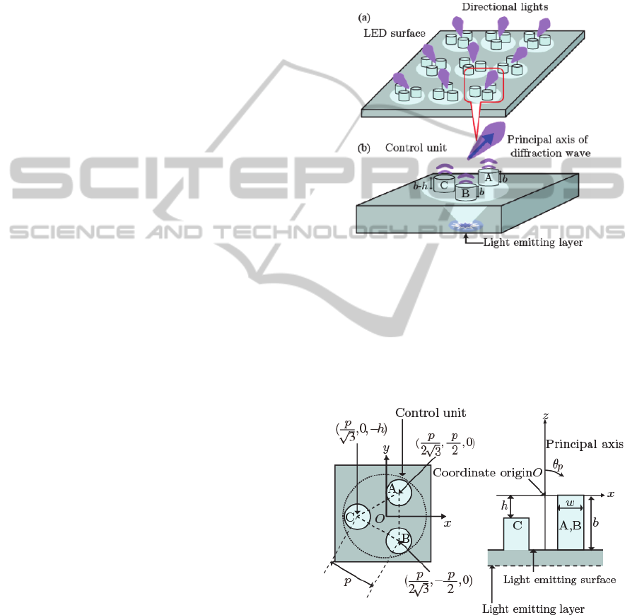
Multiple control units on an LED surface are shown
in Figure 1(a). A control unit manipulates a principal
axis toward a different direction. A single control
unit (Figure 1(b)) consists of cylinders of w in
diameter, where w is the length divided by the center
wavelength
of the LED. In this section, we
describe the dimensions in units of
, unless
otherwise stated. The cylindrical structures A, B,
and C on an LED surface and the LED are of the
same material of a refractive index n (n > 1). Heights
of structures A and B are denoted as b and that of
structure C is b - h in height. The structures are
placed on a vertex of a regular triangle p on a side,
which means their gaps are p - w. We use a system
of coordinates with their origin at the center of the
control units on the plane containing the tops of
structures A and B. The z-axis is perpendicular to
the LED surface, then the principal axis contains the
z-axis when h = 0. The x-axis is parallel to the line
from the origin to the midpoint of the center points
of structures A and B. In addition,
and
are the
horizontal and zenithal angle, as shown in Figure 2.
Figure 1: Schematics of (a) device with proposed method
and (b) directionality control unit in device array. Control
unit consists of three cylindrical structures A, B and C.
Lights from light emitting layer enter from bottom of each
structure and exits from their tops. Optical path lengths via
each structure depend on height of structures. Principal
axis, defined as direction of optical path differences via all
structures equal to zero, is controlled by difference in
height of structures h.
Figure 2: Top view and cross-sectional diagram on vertical
plane including x-axis of control unit. Cartesian coordinate
system is used with their origin at center of tops of
structures at h = 0. Z-axis is perpendicular to light emitting
surface and x-axis is parallel to line from origin to
midpoint of center points of structures A and B.
Multiple lights, which are emitted from the tops
of the structures in phase, form a diffraction pattern,
PHOTOPTICS2014-InternationalConferenceonPhotonics,OpticsandLaserTechnology
164
like hexagonally arranged spots in an image plane.
For simplicity, we assume that incident light is in
phase at the bottoms of the structures. The center
spot in the diffraction pattern corresponds to a
principal axis, whose direction is determined as that
where all of the optical path lengths from the
bottoms of the structures to the image plane are
equal.
If h is not equal to 0, the optical path length from
the bottom to the top of structure C is nh shorter than
those of structures A and B. The distance from the
top of structure C to the image plane is longer than
those from the tops of structures A and B. Because
the structures’ arrangements are in symmetry with
the xz-plane, the principal axis direction is denoted
as
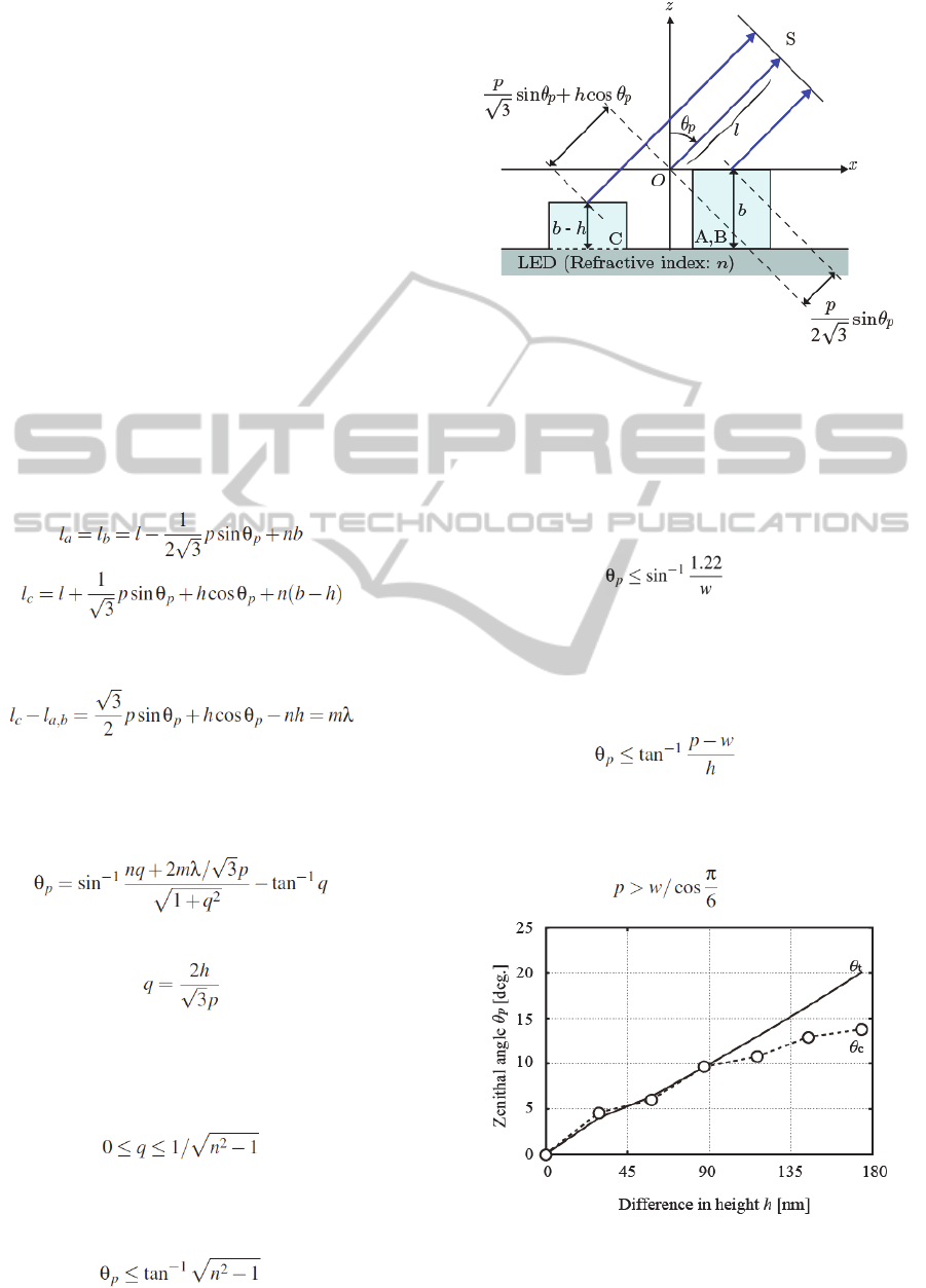
p
. We define a plane S, which is perpendicular to
the xz-plane and at a distance of l from the original
point, as the image plane, as shown in Figure 3.
Optical paths l
a
, l
b
, and l
c
from the bottoms of
structures A, B, and C to S by way of the tops of the
structures are expressed as
(1)
(2)
Then the difference in optical path lengths between
l
a
, l
b
, and l
c
are expressed as
(3)
Here, m is the optical path difference between the
lengths of l
a
, l
b
, and l
c
. The
p
of an m-th order
diffraction wave on the vertical plane including the
x-axis can be obtained by solving Equation (3).
(4)
Here,
(5)
When we assume that the principal axis direction is
given by Equation (1) at m = 0,
p
depends on
parameter q, and monotonically increases within the
following range.
(6)
However, the maximum angle of the principal axis
p
is given by Equation (7), which depends only on
the index.
(7)
Figure 3: Principal axis direction on vertical plane
including x-axis. Image plane S is l in shortest distance
from origin point and
p
in angle formed by l and z-axis.
Therefore the maximum value of
p
is constrained
by the structures’ dimensions. A principal axis
should be made within the airly patterns of the
structures. The
p
is restricted to the following range.
(8)
Too small of structure gaps p - w confine the
working range of
p
. The gap and h should satisfy
the following equation to prevent an obstruction in
the line of sight along the x-axis from the top of
structure C by another structure.
(9)
Regarding the y-direction, we use the following
condition to prevent light scattering by another
structure.
(10)
Figure 4: Principal axis angles as function h. Suffixes t
and c correspond to analytically and numerically
calculated results.
DirectionalityControlofLight-emittingDevicesthroughSub-micronDielectricStructures
165
Equation (10) suggests that the orthogonally
projected profile of a structure on the xz-plane
prevents the overlap with other structures that have
different x-coordinate values of the central axis.
These are additional conditions of structure
dimensions.
2.2 Simulation Results
In this section, we describe the basic characteristics
for the proposed method by using numerical
analysis. With the proposed method, the distance
between a light emitting surface to a light emitting
layer is several wavelengths. The wave-optics
should be used instead of the geometric optics for
analysis in the LED medium. We applied the 3D
FDTD method with a perfectly matched layer (PML)
boundary condition to verify the control function of
the proposed method.
We used InGaN-GaN LEDs as an example. The
center wave-length and full width at half maximum
(FWHM) of the spectrum were assumed to be 465
and 20 nm, and we ignored the absorption of emitted
light in the LEDs. The spectral envelop of emitted
light from the LEDs is a Gaussian shape. Therefore,
the multiple-dipole sources polarized in the xy-plane
is arranged in the light emitting layer and excited
with a Gaussian profile in time. For simplicity, the
light emitting layer is at 465 nm from the bottom of
the structures. The LED and the structures on the
light emitting surface were of the same material with
index of 2.47 (http://refractiveindex.info/).
The coordinate origin shown in Figure 2
corresponds to the position at the center of the
calculation space. The calculation space was 6 m
and accordingly discretized using 15-nm grids. The
light emitting layer was distributed inside a circle
930 nm in diameter. The dimensions of the structure
were w = 750 nm, p = 930 nm, and b = 750 nm.
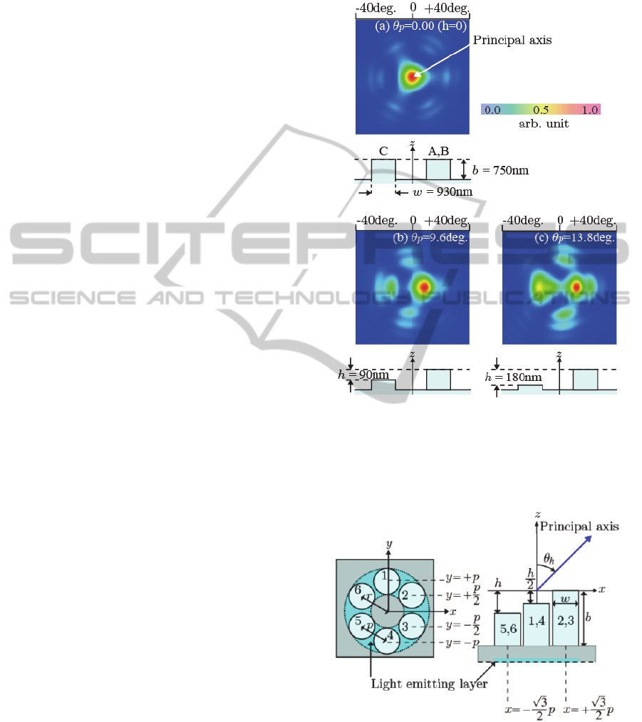
First, we discuss the calculated results of the
principal axis direction angle
p
depending on h.
Figure 4 shows the direction angles
p
. In Figure 4,
c
, indicated with a solid line, was calculated from
Equation (4);
t
, indicated with a dashed line, was
obtained from the simulation results. The calculated
direction angle
c
shows the same tendency as
t
.
Below 90nm in h, they are quantitatively the same;
above 90nm in h, the increasing tendency of
c
falls
into a sluggish pace compared with
t
. This is partly
because Equation (4) is derived without
consideration of aperture shapes. As viewed from
p
,
the shapes of the structure tops are ellipses in wcos
p
,
which is a minor axis parallel to the x-axis, and the
apparent position of structure C moves hsin
p
to the
coordinate origin. In this result, a spot of the
principal axis is expanded toward -
, and it limits
p
.
Figure 5: Field intensity distribution corresponding to h =
(a) 0, (b) 90 and (c) 180 nm, and cross-section diagram of
control unit. Images (a), (b) and (c) were calculated by
temporal integration of Poynting vector at 3000 nm from
tops of structures. Red and blue regions represent high-
and low-intensity parts of field intensity distribution.
Figure 6: Top view and cross-sectional diagram on vertical
plane including x-axis of control unit at N=6.
Next, we discuss the clarity of the principal axis
for the proposed method. Figure 5 shows field
intensity distribution corresponding to
= 0, 90 and
PHOTOPTICS2014-InternationalConferenceonPhotonics,OpticsandLaserTechnology
166
180 nm. Each image is constructed by temporal
integration of a Poynting vector at 3000 nm from the
top of the structures. In Figure 5, the high- and low-
intensity parts are represented by red and blue
regions, respectively. We also show the cross-
sectional diagram in a vertical plane. The principal
axis direction increases in step with h in Figure 5.
The principal axis becomes less clear as h increases.
This is because diffraction wave without some kind
of stray light affects the field intensity distribution.
This is an undesirable characteristic in beaming
devices. We discuss a method for obtaining a
sharply defined principal axis.
3 IMPROVED STRUCTURE
3.1 Design Rules
In this section, we describe the design rules to
improve the clarity of the principal axis based on
light use efficiency.
The principal axis consists of lights from the
light emitting layer to S via the top of the structures.
Other lights, which directly come from the light
emitting surface to S, are not involved in forming
the principal axis. Thus, a ring-shaped distribution is
acceptable as a light emitting layer distribution
profile. The inside and outside diameters of the light
emitting layer distribution should be equal to those
of the inscribed and circumscribed circles of the
structures on the light emitting surface.
The light use efficiency of the proposed method
is also affected by the number of structures. We
estimate the ratio
of light intensity via the tops of
N structures to the total amount of light intensity
from the light emitting surface. Here, N structures
are w in diameter and equally spaced on a circle
with a radius r and pitch p. This ratio is expressed as
(11)
To calculate
according to Equation (11), we
should modify Equation (10) as follows.
(12)
(13)
(14)
(15)
We then obtain
= 0.325 (N=3), 0.707 (N=4), 0.866
(N=6), and 0.541 (N=8). By comparing these values,
we obtain the maximum
at N=6. We can then
diminish excess light by using the ring-shaped
distribution profile of the light emitting layer and
use six structures.
We now describe a modification of Equation (4)
for six structures. In this case, r and p are equal. We
use p instead of r. Figure 6 shows a single control
unit of six structures. For simplicity, structures that
have the same x-coordinate value of the central axis
are the same height. Then the principal axis direction
is described as
h
. The height of structures 1, 2, 3, 4,
5 and 6 are shown in Figure 6. In this case, optical
paths l
k
(k = 1 – 6) from the bottoms of structures k
to S by way of the tops of the structure are expressed
by the following equations.
(16)
(17)
(18)
From Equations (16), (17), and (18), the differences
in optical path lengths are of three types. First, an
optical path length from a pair of structures that are
symmetric about the xz-plane is zero in the entire
area on the xz-plane. Next, if the x-coordinate value
of one of the structures is zero, the optical path
length is expressed by the following equation.
(19)
If the signs of the x-coordinate values of structures
are opposite, the optical path length is expressed by
the following equation
(20)
Equations (19) and (20) are equivalent at m=0. We
then obtain
h
by the following equation.
(21)
3.2 Simulation Results
We now explain the simulation results to diminish
excess light with the proposed method. To calculate
field intensity distribution, we used the 3D FDTD
method mentioned in Section 3. The differences
with that mentioned in Section 3 are the calculation
space size and device structure. The calculation
space was 9 m. The light emitting surface was
DirectionalityControlofLight-emittingDevicesthroughSub-micronDielectricStructures
167
covered with a metal mask to obscure light other
than from the control unit. The light emitting surface
had a hole and the control unit was arranged at the
bottom of the hole. Other calculation conditions are
listed in Table 1.
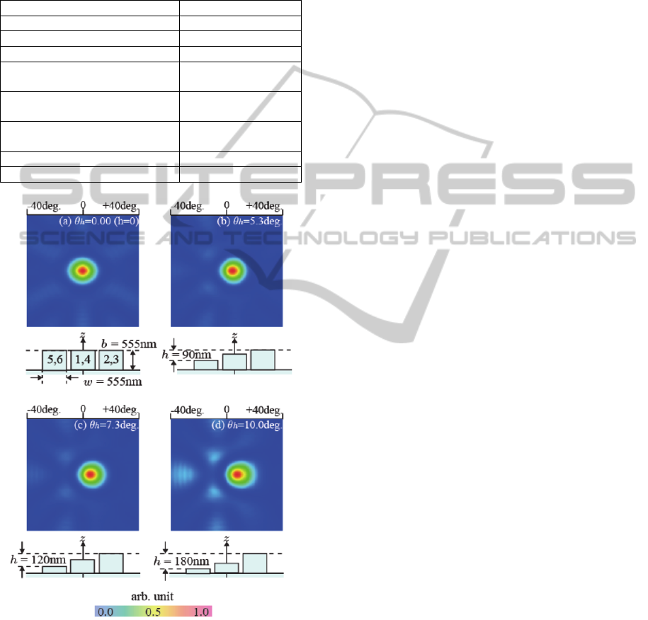
Table 1: Calculation conditions.
Diameter of structure (w) 555 nm
Pitch of structures (p) 630 nm
Height of structure (b) 555 nm
Difference in height (h) 0, 90, 180 nm
Outside diameter of
light emitting layer
1815 nm
Inside diameter of
light emitting layer
705 nm
Depth of light emitting layer
from bottoms of structures
465nm
Hole diameter 2325 nm
Metal mask thickness 135 nm
Figure 7: Field intensity distribution of control unit at N=6
corresponding to h = (a) 0, (b) 90, and (c) 180 nm. Images
(a), (b), and (c) were calculated by temporal integration of
Poynting vector at 5400 nm from tops of structures.
The field intensity distribution corresponded to h
= 0 90 and 180 nm. Each image was constructed in
the same manner as in Figure 5. However, these
images were constructed by the temporal integration
of a Poynting vector at 5400 nm from the tops of the
structures. Excess light was greatly reduced, as
shown in Figure 7. We then obtained a sharply
defined principal axis by using the improved
proposed method.
4 CONCLUSIONS
We proposed a method for controlling the principal
axis direction of LEDs and to obtain a sharply
defined principal axis through fine-structures on the
light emitting surface. We also verified the
effectiveness of the method by using the FDTD
method. In this result, a sharply defined principal
axis from a 2.3-m aperture is obtained by using the
proposed method.
The proposed method is suitable for high-density
array devices because it uses several sub-micron
dielectric structures as a means for directional
control. By applying the proposed method, high-
density beaming array devices are possible. The
method is also suitable for ray-based displays or
other applications.
We are planning to fabricate a new device with
the proposed structure by means of focused ion
beam (FIB) technique, which is promising for the
fabrication of fine structures with precise control of
height as well as in-plane dimension. For the FIB
fabrication, the structure and dimension will be
designed with FIB's characteristics taking into
account. Then, the directional control properties of
the new device will be evaluated to verify the
effectiveness of the proposed method.
REFERENCES
Krames, M. R., Shchekin, O. B. Mueller-Mach, R.,
Mueller, G. O., Zhou, L., Harbers, G., and Craford, M.,
G., 2007, “Status and Futre of High-Power Light-
Emitting Diodes for Solild-State Lighting”, IEEE
Journal of Display Technology, 3 (2), 160 - 175.
doi:10.1109/JDT.2007.895339.
McKendy, J. J. D., Massoubre, D., Zhang, S., Rae, B. R.,
Gree, R. P., Gu, E., Henderson, R. K., Kelly, A. E.,
and Dawson, M. D., 2012, “Visible-Light
Communications Using a CMOS-Controlled Micro-
Light-Emitting-Diode Array”, IEEE Journal of
Lightwave Technology, 30 (1), 61 - 67.
doi:10.1109/JLT.2011.2175090.
Sony Corp., 2012, Sony Develops Next-generation
Display, “Crystal LED Display”, Ideal for High
Picture Quality on Large screens. Full HD 55-inch
Prototype model Exhibited At 2012 International CES,
PHOTOPTICS2014-InternationalConferenceonPhotonics,OpticsandLaserTechnology
168

News releases of Jan. 10, 2012, Retrieved from:
http://www.sony.net/SonyInfo/News/Press/201201/12-
005E/
Fournier, F., Rolland, J., 2008, “Design Methodology for
High Brightness Projectors”, IEEE Journal of Display
Technology, 4 (1), 86 - 91.
doi:10.1109/JDT.2007.907110.
Tu, S. -H., Pan, J. -W., Wang, C. -M., Lee, Y. -C., and
Chang, J. -Y., 2009, “New Collection Systems for
Multi LED Light Engines”, Optical Review, 16 (3),
318 - 322.
McGroddy, K., David, A., Matioli, E., Iza, M., Nakamura,
S., DenBaars, S., Speck, J., S., Weisbuch, C., and Hu,
E., L., 2008, "Directional emission control and
increased light extraction in GaN photonic crystal light
emitting diodes", Appl. Phys. Lett., 93 (10), 103502.
Doi:10.1063/1.2978068.
Lai, C. -F., 2012, Emission aperture size limited the
guided mode extraction characteristics of GaN-based
ultrathin-film photonic crystal micro-light-emitting
diodes, Appl. Phys. Lett., 101, 023109. doi:
10.1063/1.4734509.
Son, J. -Y., Javidi, B., Yano, S., and Choi, K. -H., 2010,
“Recent Developments in 3-D Imaging Technologies”,
IEEE Journal of Display Technology, 6 (10), 394 -
403. doi:10.1109/JDT.2010.2045636.
Fattal, D., Pheng, Z., Tran, T., Vo, S., Fiorentino, M.,
Brug, J., Beausoleil, R. G., 2013, A multi-directional
backlight for a wide-angle, glasses-free three-
dimentional display, Nature, 495, 348-351.
Doi:10.1038/nature11972.
Handbook of Optics, 3rd edition, Vol. 4. McGraw-Hill
2009. Retrieved July 30, 2013, from
http://refractiveindex.info
DirectionalityControlofLight-emittingDevicesthroughSub-micronDielectricStructures
169
