
Multicasting Characteristics of All-optical Triode based on Negative
Feedback Semiconductor Optical Amplifiers
S. Aisyah Azizan, M. Syafiq Azmi and Yoshinobu Maeda
Graduate School of Science and Engineering, Kinki University, 3-4-1 Kowakae, Higashi Osaka, 577-8502, Japan
Keywords: Semiconductor Optical Amplifier, Multicasting, Wavelength Conversion, Optical Triode, Negative
Feedback Optical Amplifier, Cross Gain Modulation.
Abstract: We introduce an all-optical multicasting characteristics with wavelength conversion based on all-optical
triode using two negative feedback semiconductor optical amplifiers at a transfer speed of 10 Gbps to a non
return zero 2
31
-1 pseudorandom bit sequence system. This multi-wavelength converter device can
simultaneously provide two channels of output signal with the support of non-inverted and inverted
conversion. We reported an all-optical multicasting and wavelength conversion accomplishing cross gain
modulation is effective in a semiconductor optical amplifier in order to provide an inverted conversion thus
negative feedback. The relationship of received power of back to back signal and output signals with
wavelength 1530 nm, 1540 nm, 1545 nm, 1555 nm, and 1560 nm with bit error rate was investigated. It was
found that the output signal wavelengths were successfully converted and modulated with a power penalty
of less than 5 dB which the highest is 4.7 dB while the lowest is 2.2 dB. It was realized that all-optical
multicasting and wavelength conversion using an optical triode with a negative feedback by two channels at
the same time at a speed of 10 Gbps is possible.
1 INTRODUCTION
Demand for the wavelength division multiplexing
(WDM) in wider band has progressed especially in
the future technology of photonic networks. As the
cost and power consumption of WDM network
nodes are in a large amount, it is essential to discard
the conventional optical/electrical/optical (O/E/O) to
optical/optical (O/O) by using all-optical wavelength
converter device. Optical wavelength conversion is
anticipated to be an essential function for the
emerging bandwidth-intensive applications (video
conferencing, video-on-demand services etc.) of
high speed WDM optical networks by enabling rapid
resolution of output-port contention and wavelength
reuse (Y. Yuang et al., 2000).
In addition, all-optical wavelength converter
becomes a key functional element in WDM optical
network due to its capabilities of transparent
interoperability, contention resolution, wavelength
routing and, in general, better utilization of the fixed
set of wavelengths (J. M. H. Elmirghani and H. T.
Mouftah, March 2000).
Nowadays, multicasting is a potentially useful
networking function that involves the same data
stream from a single node to several destinations
nodes. This network is also called as photonic
network. Photonic network is commonly enforced
via IP digital routers in electrical domain. Photonic
network effectiveness will be encouraged when the
multicasting can be performed all-optically. The
optical routers will be able to multicast an input
signal to different wavelengths.
There is bulk of wavelength conversion and
multicasting techniques that have been proposed so
far. The techniques include a nonlinear
semiconductor optical amplifier (SOA) based
interferometer, an injection locking of a Fabry-Perot
laser (C. W. Chow et al., 2003), and SOA with cross
gain modulation (XGM) or SOA with cross phase
modulation (XPM) (M. Matsuura, N. Kishi, and T.
Miki, 2006). In this paper, we investigated the new
wavelength converter technology technique based on
the negative feedback optical amplification effect.
This will result an output signal whose gain,
waveform, and, baseline which stabilized
automatically. Wavelength conversion and switching
characteristics was investigated by introducing a
control light together with input signal light (Y.
Maeda and L. Occhi, 2003).
170
Azizan S., Azmi M. and Maeda Y..
Multicasting Characteristics of All-optical Triode based on Negative Feedback Semiconductor Optical Amplifiers.
DOI: 10.5220/0004708301700174
In Proceedings of 2nd International Conference on Photonics, Optics and Laser Technology (PHOTOPTICS-2014), pages 170-174
ISBN: 978-989-758-008-6
Copyright
c
2014 SCITEPRESS (Science and Technology Publications, Lda.)
The optical amplifier consists of an InGaAsP/InP
SOA and an optical add/drop filter. It is equipped
with a negative feedback function. In the negative
feedback SOA, the output modulation degree will be
substantially higher and the distortion of the
waveform was extremely small in wide input signal
(Y. Maeda, 2011). We demonstrated the conversion
wavelength by using two SOAs based on optical
triode, and measured the bit error rate (BER)
characteristics for each wavelength. As a result, this
device has been realized that all-optical multicasting
and wavelength conversion by using two channels at
the speed of 10 Gbps at the same time is possible.
1.1 Negative Feedback Optical
Amplification
As mentioned above, negative feedback optical
amplifier consists of a SOA and an optical add/drop
filter. The basic theory of negative feedback is
explained below.
SOA is structured based on the ridge waveguide
of InGaAsP/InP material. The composition of the
InGaAsP active layer is chosen to have gain peak
wavelength around 1550 nm. The maximum small
signal fiber to fiber gain is around 15 dB and the
output saturation power is approximately 2 mW
measured at 1550 nm with a bias current of 250 mA
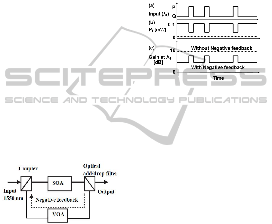
(Y. Maeda, 2011). Figure 1 shows the diagram of a
negative feedback SOA circuit.
Figure 1: Block diagram of a negative feedback SOA.
VOA: Variable optical attenuator.
As shown in Figure 1, a wavelength of 1550 nm
is set as an input signal by a tunable laser then is
modulated by the mean of electro-optic modulator.
The modulated input signal is fed into the SOA by
using a coupler. An optical add/drop filter is located
in order to extract an output signal light of the
wavelength 1550 nm. The XGM mechanism in SOA
will provide the spontaneous emission contain an
inverted replica of the information carried by input
signal. The inverted replica information is fed back
and injected together with the input signal back into
the SOA by using a coupler. The output average
power was around 6.4 mW, which the SOA was
without negative feedback while in the SOA with
negative feedback, the output average power was
approximately 1.9 mW. These were experimented
when the negative feedback average power was 0.12
mW (Y. Maeda, 2011).
Figure 2: Concept diagram of negative feedback optical
amplification effect.
Figure 2 shows the concept diagram of a
negative feedback optical amplification effect. The
straight-line represents the case where the SOA was
used with negative feedback while the dotted line
represents the case of the SOA without negative
feedback.
Figure 2(a), (b), and (c) show the waveforms of
the input signal, the negative feedback, and the gain
in SOA respectively. In the SOA that has a XGM
mechanism, spontaneous emission lights, which
have wavelengths near a wavelength λ
ଵ
, the input
signal have an intensity varying in response to a
variation in the intensity of that input signal.
Characteristically, the intensity variation of the
spontaneous emission lights are inverted with
respect to the variation in the input signal then the
spontaneous emission lights are outputted from the
SOA as reported in Figure 2(b).
In the past, it is common that the spontaneous
emission lights as well as the surrounding light that
have wavelengths other than the wavelength λ
ଵ
are
removed by a band pass filter, since it becomes a
factor of noise generation (Y. Maeda, 2011). In this
situation, a negative feedback optical signal
amplification phenomenon in which characteristics
of the gain of the SOA is drastically changed by
feeding back the separated surrounding light to the
SOA so that the gain is modulated as shown in
Figure 2(c). Therefore, noise reduction is realized
all-optically with a negative feedback SOA. It can be
concluded that the output signal waveform is
MulticastingCharacteristicsofAll-opticalTriodebasedonNegativeFeedbackSemiconductorOpticalAmplifiers
171

exceptionally improved over that without negative
feedback. In addition, the baseline of the output
signal waveform is supressed because the gain in the
SOA is low when the power of input signal is at the
low logical level, whereas the output signal is
stressed because of the high SOA gain when the
input signal power is high as shown in Figure 2 (Y.
Maeda, 2011). In this paper, we created an all-
optical triode based on the negative feedback SOA
theory.
2 OPERATION PRINCIPLE
The experimental setup is reported in Figure 3. The
operating circuit of negative feedback optical
amplification by using optical triode is explained as
follows.
In this experiment, we used full band thermally
tunable distributed-feedback (DFB) laser diode
module. The isolator from the device has been taken
out in purpose to allow any reflection of the signal
light from the SOA. This device is used as the SOA
and laser diode (LD) as shown in Figure 3. We
created an optical triode by using two SOAs forming
two stages of SOAs, SOA-1 for the first stage and
SOA-2 for the second stage of the circuit with two
optical add/drop filters (1550 nm േ 6.5 nm).
An optical signal that has been modulated by the
external optical modulator (O.M) enters the SOA-1
via an optical add/drop filter (1550 nm േ 6.5 nm).
Due to the XGM mechanism in SOA-1, the probe
light, which is set in the SOA-1, is modulated into a
signal then provide the spontaneous emission
contain an inverted intensity to the optical signal
which fed in SOA-1. This inverted optical signal
then passes through an optical add/drop filter (1550
nm േ 6.5 nm) thenceforth it flew into the SOA-2
based on the negative feedback theory. The input
signal is amplified with gain modulation by inverted
optical signal in the SOA-2.
In this research, an optical signal with
wavelength 1552 nm is set by a laser source as the
input signal. This optical signal is modulated to a
non return zero (NRZ) 2
31
-1 pseudorandom bit
sequence (PRBS) with a transfer speed of 10 Gbps
by the O.M then is amplified by the Erbium doped
fibre amplifier (EDFA) before fed into the optical
triode. Additionally, probe light with wavelength of
1551 nm is set in SOA-1.
In order to perform multicasting in wavelength
conversion through this experiment, two different
wavelengths are set as the control signal in SOA-2.
Five different wavelengths are chosen as the control
signal to be used in this research. They are 1530 nm,
1540 nm, 1545 nm, 1555 nm, and 1560 nm. These
control signals (two wavelengths at a time) will be
fed into the SOA-2, which have undergone XGM
and wavelength conversion is occurred.
Consequently, the two different optical signals will
be amplified by the SOA-2 thus pass through an
optical add/drop filter. After that the optical signals
passed a VOA and a band pass filter (BPF).
As the two control signals are in different
wavelengths, a BPF is needed for wavelength
separation to recognize the output signals.
Thenceforth, the optical signals are inserted into the
bit error rate tester (BERT) hence the relationship of
received power of back to back signal (B to B
signal/BER of input signal) and output signals which
is controlled by the VOA, with BER is measured.
Figure 3: Experimental setup.
3 RESULTS AND DISCUSSION
Figure 4 shows the eye diagrams obtained in this
experiment. Figure 4(a) shows the input signal eye
diagram whereas (b), (c), (d), (e), and (f) show the
eye diagram for output signals of 1530 nm, 1540
nm, 1545 nm, 1555 nm, and 1560 nm respectively.
The eye diagram of input and output signals are
recorded when their average power is 150 μW. Zero
level from baseline (from ground) of input signal is
BERT
LASER
SOURCE
EDFA
O.M
SOA-1
LD
SOA-2
LD
VOA
Probe
1551 nm
Inverted signal
Input Signal
1552 nm
BPF
Optical
add/drop filter
Optical
add/drop filter
Control signal:
1530 nm, 1540 nm,
1545 nm, 1555 nm,
1560 nm
BPF
Optical Triode
PHOTOPTICS2014-InternationalConferenceonPhotonics,OpticsandLaserTechnology
172
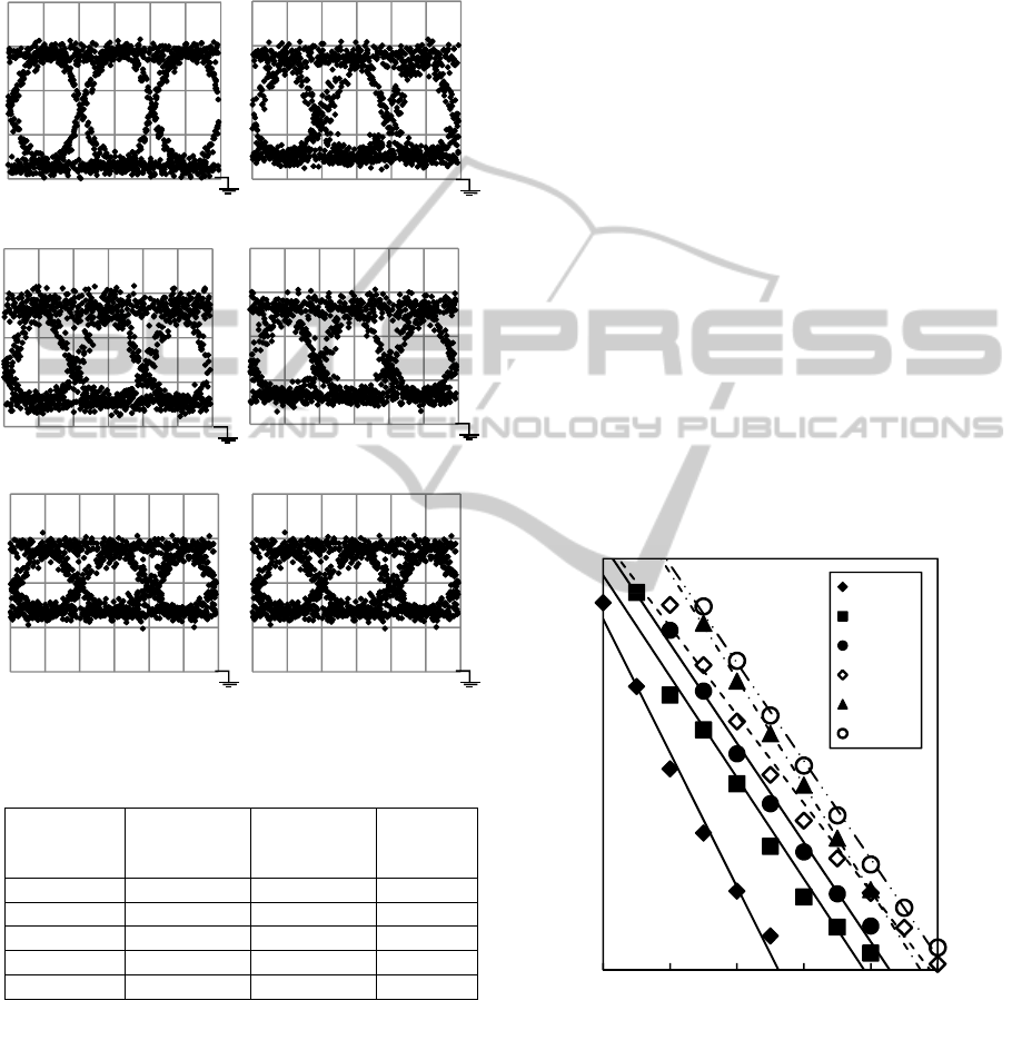
27 μW. Eye aperture, extinction ratio and zero level
from the baseline of each output signal eye diagram
are measured and are summarized in Table 1.
(a) Input (b) 1530 nm
(c) 1540 nm (d) 1545 nm
(e) 1555 nm (f) 1560 nm
Figure 4: Eye diagrams of input and output signals
(50μW/div, 50ps/div).
Table 1: Summarization of measurement result.
Wavelength
[nm]
Eye
aperture
[dB]
Extinction
ratio [dB]
Zero
level
[μW]
1530 4.35 7.39 49
1540 3.90 6.97 54
1545 3.45 6.19 63
1555 2.22 4.40 83
1560 2.12 4.28 84
As reported in Figure 4, the baseline of output
signal eye diagrams arose gradually compared to the
input signal eye diagram. Based on Table 1, the zero
level from baseline of output signals increase when
the wavelength becomes longer, from 1530 nm to
1560 nm. In addition, the degradation in eye
aperture of output signals is clearly reported in
Figure 4 and Table 1. The obtained results show that,
the highest extinction ratio is 7.39 dB when the
output signal wavelength is 1530 nm.
Based on the reported results, it proved that
during the conversion of wavelength conducted in
the SOAs consumed large amount of power and
noise has been found due to the distortion of the eye
diagrams as clearly shown in Figure 4 especially in
Figure 4(e) and (f). We understood that a
conventional optical amplifier merely has a simple
amplification function that is almost constant gain.
The amplifier disadvantageously amplifies not only
the signal but also the noise. Therefore, the eye
diagram and baseline of the output signal cannot be
improved basically in relation with the noise,
thereby making difficult to achieve an advanced
signal processing. In spite of all, it is understood that
the eye aperture of optical signals declines as the
wavelength increases. In Figure 4, we conclude that
1530 nm has the highest eye aperture compared to
the other output signals.
In order to assess multicasting characteristics, we
measured the relationship between received power
and BER and reported in Figure 5. We have
measured the BER for B to B signal (also called
back to back signal), output signals 1530 nm, 1540
nm, 1545 nm, 1555 nm, and 1560 nm.
Figure 5: Result of bit error rate test.
It was found that the smaller the received power
of the signals, the bigger the BER will be. We
studied that it may be an effect of the dependence of
the speed propagation light through the medium
during the conversion of wavelengths that produce
errors. From the result of BER test, relationship of
-34,0 -32,0 -30,0 -28,0 -26,0 -24,0
Log
10
(BER)
Received Power [dBm]
B to B
1530 nm
1540 nm
1545 nm
1555 nm
1560 nm
-12
-10
-8
-4
-2
-6
MulticastingCharacteristicsofAll-opticalTriodebasedonNegativeFeedbackSemiconductorOpticalAmplifiers
173

power penalty with respect to B to B and control
signals when the BER is 10
-9
is summarized. The
summarization result is shown in Figure 6.
It is understood that the BER and power penalty
with respect to B to B signal become worse as the
control signal wavelengths increase. Figure 6
reported that we obtained power penalty that less
than 5 dB. The highest power penalty is 4.7 dB
when the control signal is 1560 nm while the lowest
is 2.2 dB when the control signal is 1530 nm.
Therefore, we found that BER for output wavelength
of 1530 nm is the nearest to the B to B signal than
output wavelengths of 1540 nm, 1545 nm, 1555 nm,
and 1560 nm.
Figure 6: Relationship of power penalty with respect to B
to B and control signal.
4 CONCLUSIONS
We investigated multicasting characteristics by
using an optical triode, which has been set up with
two stages of SOAs that constitute a negative
feedback optical amplifier with two optical add/drop
filters. Based on the BER measurement result,
output signal of 1530 nm produced the least error
compared to the other output signals after undergone
wavelength conversion. Thereby, we concluded that
1530 nm has the smallest power penalty than the
other output signals when the BER is 10
-9
.
Therefore, we understood that when the wavelength
becomes longer, the BER becomes worse. Hence,
this device also proved that all-optical multicasting
and wavelength conversion with two channels at a
time with a transfer speed of 10 Gbps is possible.
Furthermore, we found out that, by this
experiment, it is possible to achieve negative
feedback optical amplification by SOA with the
insertion of input and control signal into the SOA. It
also proved that the conversion of wavelength
(O/E/O) through electronic circuit can be innovated
to all-optical signals (O/O) and are applicable in our
optical triode.
Multicasting characteristics are recognized and
the conversion of one wavelength to another
different wavelength by injecting input and control
signal with a speed of 10 Gbps at the same time in
this device has been proved.
ACKNOWLEDGEMENTS
This work was supported in part by the Ministry of
Education, Culture, Science and Technology of
Japan, a Grant-in-Aid (21560048) for scientific
research ©.
REFERENCES
Y. Yuang et al., 2000. Nonblocking WDM multicast
switching networks, IEEE Trans On Parallel and
Distrib. Sys., pp. 1274-1287.
J. M. H. Elmirghani and H. T. Mouftah, March 2000. All-
optical wavelength conversion: Technologies and
applications in DWDM networks, IEEE Commun.
Mag., vol. 38, pp. 86-92.
C. W. Chow et al., 2003. 8ൈ10 Gb/s multiwavelength
injection locking of a FP laser diode for WDM
multicast, Proc. Of IEEE LEOS, pp. 682-683.
M. Matsuura, N. Kishi, and T. Miki, 2006. Broadband
regenerative wavelength conversion and multicasting
using triple-stage semiconductor-based wavelength
converters, IEEE Photon. Technol. Lett., pp. 2659.
Y. Maeda and L. Occhi, 2003. All-optical triode based on
a tandem wavelength converter using reflective
semiconductor optical amplifiers, IEEE Photonics.
Technol. Lett., pp. 257.
Y. Maeda, 2011. Advances in Optical Amplifiers, Paul
Urquhart ed. INTECH Open Access, pp. 231-252.
0
1
2
3
4
5
6
7
1525 1535 1545 1555 1565
Power penalty (dB)
Control signal (nm)
PHOTOPTICS2014-InternationalConferenceonPhotonics,OpticsandLaserTechnology
174
