
F
2
-Laser Microfabrication of Diffractive Phase Elements
M. Pfeifer, F. Jahn, A. Kratsch, B. Steiger and S. Weissmantel
University of Applied Sciences Mittweida, Technikumplatz 17, 09648 Mittweida, Germany
Keywords: DPE, Diffractive Phase Element, DOE, Diffractive Optical Element, Fluorine Laser, Mask Projection.
Abstract: Fluorine laser microfabrication enables direct structuring of diffractive phase elements in fused silica. These
elements are used as beam shapers for the wide wavelength range from 248 to 1100 nm. We present
selected phase elements for laser beam shaping in the visible wavelength range. Furthermore we show the
laser beam shaping of a fiber laser with a wavelength of λ = 1070 nm. The main advantage of this
application is the much more compact design compared with the current used method of beam shaping by
conventional optics. Fluorine laser microstructuring provides an effective alternative to lithography
techniques. It is a fast and individual method to fabricate customized or prototype diffractive phase elements
in a cost-effective way.
1 INTRODUCTION
Beam shaping by diffractive phase elements (DPEs)
is currently one of the most important fields of
research on optics with almost the greatest potential
in application and innovation. In the future it will be
possible to shape any beam profile into almost every
desired beam distribution. In this way DPEs enable
the homogenization of laser beams. The main
advantage of this application is the much more
compact design compared with the current used
method of beam homogenization by conventional
optics. Furthermore, it is conceivable to design
special DPEs shaping the raw laser beam directly
into the desired beam geometry for the working
plane. In this way, masks are no longer needed. Thus
the laser power can be used more efficiently by
using the full beam cross-section.
The manufacturing of DPEs is mainly done by
photolithography. This technique is very complex,
because it has to be done in several photolithography
steps. Also it requires a various number of masks
due to the desired number of steps of the DPE. Laser
microstructuring using a mask projection technique
opens up a new way. It is a fast and individual
technique to fabricate customized or prototype
diffractive phase elements in a cost-effective way.
This is possible because, for instance, compared
with photolithography there are no special masks
necessary, which have to be manufactured for each
new DPE. Also there is only one mask needed,
because of the pixelwise structuring process. The
microstructuring is done by pulsed laser ablation
using a fluorine laser. Because of its short
wavelength in the VUV range, it enables
micromachining of wide band gap materials such as
fused silica. Furthermore, calcium fluoride is used as
material for beam shapers for the excimer laser
wavelength 157 nm and 193 nm. However, this
material is very difficult to structure by lithography
techniques because of its material properties.
Fluorine laser microstructuring provides an effective
alternative at this point.
2 F
2
-LASER STATION
The microstructuring is done by a fully automated
high-precision laser micromachining station. It was
developed and built by 3D-Micromac AG in
cooperation with the University of Applied Sciences
Mittweida. A fluorine laser LPF 220i of Coherent
(Deutschland) GmbH is integrated in this station.
The laser beam has a wavelength of 157 nm that
corresponds to a photon energy of 7.9 eV. The
maximum repetition rate is 200 Hz and the pulse
duration is 25 ns. The pulse energy can be varied
from 10 to 30 mJ. Because of the wavelength in the
VUV range, the beam guidance must take place in
an oxygen-free atmosphere. The special advantage
of the used laser station is a system of two
independent vacuum chambers. After evacuation
91
Pfeifer M., Jahn F., Kratsch A., Steiger B. and Weissmantel S..
F2-Laser Microfabrication of Diffractive Phase Elements.
DOI: 10.5220/0004713600910096
In Proceedings of 2nd International Conference on Photonics, Optics and Laser Technology (PHOTOPTICS-2014), pages 91-96
ISBN: 978-989-758-008-6
Copyright
c
2014 SCITEPRESS (Science and Technology Publications, Lda.)

these chambers are flooded with pure nitrogen (5.0)
to normal pressure.
The laser microstructuring is done by mask
projection technique. Here the mask geometry is
optically imaged onto the substrate surface by a
transmission objective with a demagnification ratio
of 26 : 1. The maximum structure size on the
substrate surface is about 225 x 225 µm² with a
resolution of < 1 µm. The maximum possible laser
pulse fluence on the substrate surface is about
7 J/cm².
3 DESIGN OF DIFFRACTIVE
PHASE ELEMENTS
Diffractive phase elements are a special kind of
diffractive optical elements. The active principle is
the modulation of the phasing of the electromagnetic
wave. The phase displacement between the points on
the wave front is provided by different optical path
lengths, which is achieved by structuring of different
step heights. This leads to the intended diffraction
effects and therefore to the generation of defined
diffraction images. Fused silica is used as substrate
material because of its good transmission properties
over a wide spectral range.
The calculation of the DPEs is based on a variant
of the well know POCS-method (projection onto
convex sets) (Ersoy, 2007). Here the given field
strength distributions are addressed as boundary
conditions at the DPE and pictorial space. Both, the
input-sided intensity distribution and the distribution
in the target plane, i.e. the desired diffraction image,
must be given. The transition between the spaces is
mathematically done by propagation operators. The
most frequently used operator is the Fourier
transformation and the inverse Fourier
transformation, respectively. Therefore, this
procedure is state of the art in various versions as so-
called iterative Fourier transform algorithm (IFTA)
(Fienup, 1982; Ripoll, Kettunen and Herzig, 2004;
Kim, Yang and Lee, 2004). The convergence of this
algorithm thereby depends on various parameters. A
good result for the phase distribution of the intended
DPE is reached after approximately 30 iteration
steps.
A detail of such a phase distribution is shown in
Figure 1. Here a defined phasing is assigned to each
gray value. The phase distribution of the DPE is
completely irregularly based on the unsymmetrical
intensity distribution in the target plane.
Figure 1: Detail of the phase distribution and target
structure of a nine level DPE producing the logo of the
University of Applied Sciences Mittweida (array of
128 x 128 pixels).
The original quasi-continuously calculated
distribution is discretized during the algorithm both
in its allocation and regarding to the possible
phasing. This creates the shown pixel-like structure.
This discretization is due to the properties of the
manufacturing technology. The higher diffraction
orders indicated in Figure 2 are a disadvantage of
this simplification. This leads to a loss of power in
laser beam shaping.
The applying of the Fourier transformation as
propagation operator between DPE and pictorial
space creates so-called Fourier elements. Their
diffraction image is basically formed in the far field
in infinite distance. However, a distance which is
very large towards the pixel size becomes practically
sufficient. In the academic literature different criteria
are defined for the quantitative determination of the
minimum distance (Lipson, Lipson and Tannhauser,
1997; Träger, 2007). Such DPEs are used for
alignment applications because of their almost
constant image quality over long distances.
With special regard to the practical application of
laser beam shaping for laser material processing
often there is defined a clear target plane, in which
the desired image should be formed sharply. This is
done by additional phase terms, which allow a
further manipulation of the diffraction image. For
instance, a spherical lens term enables the sharply
image formation in a defined target plane.
Figure 2 shows the simulated diffraction image
of a DPE producing the logo of the University of
Applied Sciences Mittweida in different projection
distances. The phase distribution of this DPE
contains a spherical lens term with a focal length of
300 mm. As a result the diffraction image is formed
PHOTOPTICS2014-InternationalConferenceonPhotonics,OpticsandLaserTechnology
92

sharply only in the focus. The absolute size of the
created structure depends on the projection distance.
Figure 2: Simulated diffraction image of a nine level DPE
producing the logo of the University of Applied Sciences
Mittweida (array of 256 x 256 pixels, pixel size:
7.8 x 7.8 µm
2
, design wavelength: 532 nm) with a
spherical lens term with a focal length of 300 mm in a
projection distance of (a) 0.1 m, (b) 0.3 m, and (c) 1 m.
The simulation of the shown diffraction images
is done by numerical simulation software based on
the real expected DPE structures. Therefor beside
VirtualLab
TM
5.3 of LightTrans GmbH also self-
created program scripts for MATLAB
®
of
MathWorks are used. Here the advantage is, beside
the possibility of control, that the influence of
different parameters on the formed diffraction image
of the DPE can be examined. In this way the cost-
intensive manufacturing of many different DPEs by
the trial-and-error method is no longer necessary.
Beside the elementary parameters pixel size,
number of pixels, and number of steps, a major
impact on the final diffraction image is particularly
caused by manufacturing-related deviations from the
ideal calculated phase distribution. Fluctuations of
the laser fluence during the structuring process result
in deviations in the structure depth. Form deviations
of the pixels are due to defects in the imaging
system. Based on these deviations the quality of the
diffraction image declines, which is shown by
Olbrich, Fischer and Steiger (2012). An essential
characteristic of that is the formation of an intensive
peak in the middle of the diffraction orders.
Figure 3: Simulated diffraction image of a DPE having
regard to real manufacturing faults: (a) fluctuations of the
laser fluence, (b) bars between the pixels, and (c) rounded
pixel corners.
Figure 3 shows the influences of the deviations
on the known diffraction image of the university
logo. Not only incorrect structure depth (see
Figure 3(a)), but also bars between the pixels (see
Figure 3(b)) and rounded corners of the normally
quadratic pixels (see Figure 3(c)) alter the diffraction
image. In these figures the formation of the centered
peak is clearly visible in each diffraction order.
Furthermore, Olbrich, Fischer and Steiger (2012)
show that surface roughness and process-related
debris on the DPE surface lead to an increased
background noise in the surrounding of the zeroth
diffraction order. Practically a mixture of the shown
phenomena can be expected according to the
influence of each error at the manufacturing process.
Such an intensity peak is absolutely
counterproductive for beam shaping for laser
material processing. Thus strategies have to be
developed to completely prevent these peaks or at
least to reduce their negative effects. A possible
approach could be the method of CO
2
laser
smoothing mentioned below. Another possibility
consists in the use of the already mentioned
additional phase terms. The separation of the target
structure from the centered peak is possible by using
a linear wedge term, which causes a shift of the
target structure by a defined angle.
The theoretical phase modulations must be
transferred into an appropriate form to manufacture
the designed DPEs by fluorine laser
microstructuring. Therefor, the determined phase
information is transferred to be structured depth for
each pixel according to the design wavelength and
the refractive index of the substrate. The fluorine
laser microstructuring of the DPEs is done with
masks out of tantalum foil with quadratic aperture.
Here the mask size is selected according to its image
size in the working plane, which corresponds to the
desired pixel size.
4 RESULTS AND DISCUSSION
4.1 DPEs with a Lens Term for
Λ = 532 Nm
The DPEs are structured in Corning 7980 (fused
silica). They have nine levels with a structure height
of 120 nm per step, designed for a wavelength of
λ = 532 nm. Figure 4 shows an optical micrograph
of a DPE producing the logo of the University of
Applied Sciences Mittweida.
Figure 5 shows the diffraction image of this DPE
in a projection distance of 1.68 m.
The target structure is clearly visible, but the
diffraction orders are overlaid by a centered peak.
F2-LaserMicrofabricationofDiffractivePhaseElements
93
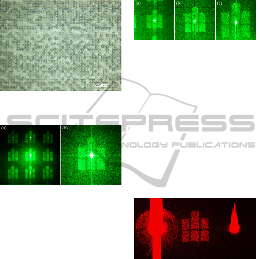
Figure 4: Optical micrograph of a nine level DPE
producing the logo of the University of Applied Sciences
Mittweida (array of 256 x 256 pixels, pixel size:
7.8 x 7.8 µm
2
, design wavelength: 532 nm).
Figure 5: Diffraction image of the DPE shown in Figure 4
in a projection distance of 1.68 m.
The main cause is an overlaid diffraction grating
based on undesirable bars between the pixels.
Basically, their formation can be averted. The
formation of the higher diffraction orders is due to
the discretization of the DPEs in the pixel-like
structure, as mentioned before. This was already
shown in the simulation. The formation of these
diffraction orders can only be avoided by a
continuous transition of the height profile.
The DPE shown in Figure 4 is calculated with an
image formation in the infinite. The function of a
DPE with lens term is shown in Figure 6. This DPE
differs to the previous by an additional spherical lens
term with a focal length of 300 mm (cf. Figure 2).
The diffraction image is shown in different
projection distances.
The real diffraction images are similar to the
simulated ones. It becomes clear, that just like in the
simulation the diffraction image becomes blurred
faster towards a shorter projection distance than
towards a longer one.
A comparison of the diffraction images in
Figure 5(b) and Figure 6(b) shows, that the
Figure 6: Diffraction image of the DPE described in
Figure 2 in a projection distance of (a) 0.2 m, (b) 0.3 m,
and (c) 1 m.
diffraction image of the DPE with lens term is more
detailed and has sharper contours than the DPE
without a lens term. Thus the partially blur of the
diffraction image of the DPE without a lens term is
not caused by a worse structuring. The diffraction
image should be captured in a longer projection
distance.
4.2 DPE with a Wedge Term for
Λ = 633 Nm
To separate the target structure from the centered
peak, a DPE with a linear wedge term was
structured. It is an eleven level DPE with a structure
height of 120 nm per step, designed for a
wavelength of λ = 633 nm. The target structure of
this DPE is the same as before. It is also designed
with an additional spherical lens term, but with a
focal length of 320 mm.
Figure 7: Diffraction image of an eleven level DPE
producing the logo of the University of Applied Sciences
Mittweida (array of 256 x 256 pixels, pixel size:
10 x 10 µm
2
, design wavelength: 633 nm) with a spherical
lens term with a focal length of 320 mm and a linear
wedge term captured in focus.
The diffraction image of the DPE is shown in
Figure 7. The target structure is shifted by a defined
angle and therefore it is completely separated from
the centered peak. The red stripe on the left side of
the image is not a part of the diffraction image. It is
a saturation effect of the CCD sensor. Also the
circular halo effect is a result of undesired
reflections at the beam expander.
PHOTOPTICS2014-InternationalConferenceonPhotonics,OpticsandLaserTechnology
94
4.3 Beam Shaper for a Fiber Laser
with Λ = 1070 Nm
Based on the investigations above a DPE was
manufactured to shape a fiber laser beam with a
wavelength of λ = 1070 nm into the known target
structure. The DPE has 19 levels with a structure
height of 120 nm per step. The DPE is designed with
an additional spherical lens term with a focal length
of 100 mm and a linear wedge term.
Figure 8: Diffraction image of a 19 level DPE producing
the logo of the University of Applied Sciences Mittweida
(array of 160 x 160 pixels, pixel size: 22.3 x 22.3 µm
2
,
design wavelength: 1070 nm) with a spherical lens term
with a focal length of 100 mm and a linear wedge term
captured in focus.
The diffraction image of the DPE is shown in
Figure 8. The centered peaks are not very
pronounced due to a reducing of the undesirable bars
between the pixels. There is only some background
noise in the surrounding of the zeroth diffraction
order, as mentioned before. Thus the laser beam
shaping for an ytterbium-doped fiber laser was
successfully done.
Besides a DPE for laser beam shaping of a diode
laser with a wavelength of λ = 940 nm was
manufactured. It was already tested at a laser power
up to 1 kW in cw mode for a short time without any
damage of the DPE.
4.4 CO
2
Laser Smoothing of DPEs
Bars could occur between the pixels, as mentioned
in chapter 4.1. These undesirable bars have a
negative impact on the diffraction image so far as
they produce a diffraction image of the raw laser
beam. This second diffraction image overlays the
desired ones (cf. Figure 5(a)). Another problem is a
roughening of the surface caused by the laser
microstructuring process. This leads to a blur of the
diffraction image. Both the reducing of the surface
roughness and the removal of the undesirable bars is
done by temperature controlled CO
2
laser
smoothing.
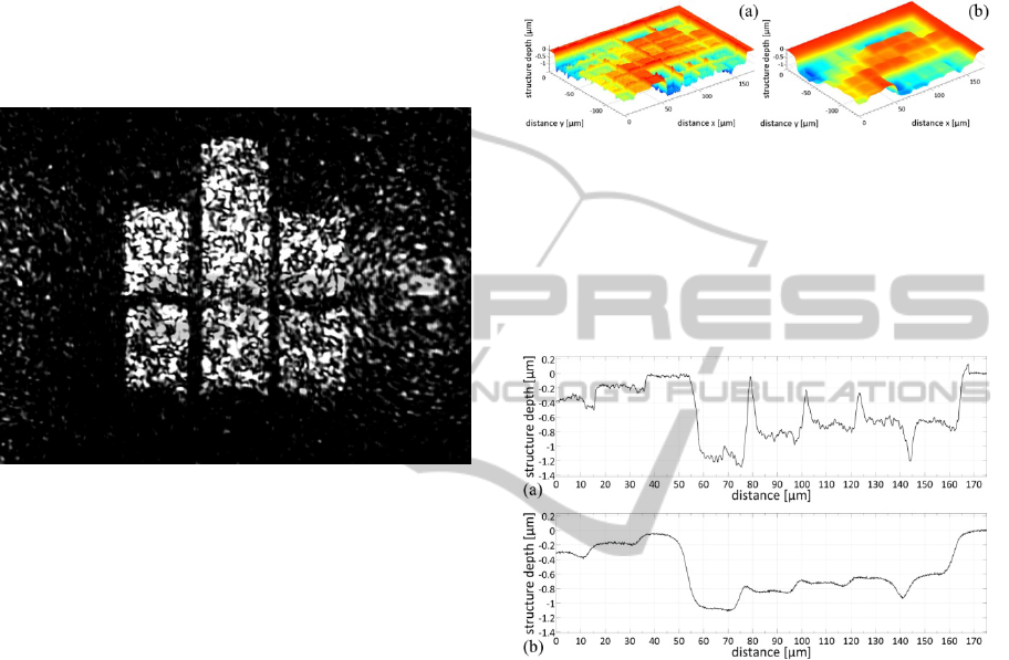
Figure 9: Three-dimensional confocal micrograph of a
DPE producing an “F” (array of 50 x 50 pixels, pixel size:
21 x 21 µm
2
, design wavelength: 532 nm) (a) before and
(b) after CO
2
laser smoothing.
Figure 9 shows the confocal micrograph of the
DPE before and after CO
2
laser smoothing. The
related profiles are shown in Figure 10.
Figure 10: Profile of selected pixels of the DPE shown in
Figure 9 (a) before and (b) after CO
2
laser smoothing.
The success of the technique is clearly visible.
The undesirable bars between the pixels are almost
completely removed. The quadratic surface
roughness could be improved from S
q
= 44.9 nm to
S
q
= 20.3 nm. These are averaged values over 25
pixels with different structure depths. The roughness
depends on the structure depth. The roughness of the
unstructured surface is S
q
= 8.9 nm.
The diffraction image of the DPE before and
after CO
2
laser smoothing is shown in Figure 11.
A comparison of Figure 11(a) and Figure 11(c)
shows, that the centered peaks are only weakly
visible due to the removing of the undesirable bars
between the pixels. Also the higher diffraction
orders are less pronounced after smoothing, which
comes along with an increase of the laser beam
intensity in the zeroth diffraction order. As this
diffraction order is more pronounced and has sharper
F2-LaserMicrofabricationofDiffractivePhaseElements
95
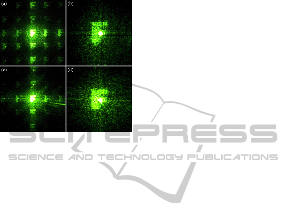
Figure 11: Diffraction image of the DPE shown in
Figure 9 in a projection distance of 1 m (a), (b) before and
(c), (d) after CO
2
laser smoothing.
contours, which can be seen in Figure 11(d)
compared with Figure 11(b). This effect is due to a
redistribution of the glass by the CO
2
laser
smoothing. Thus the edges of the pixels are rounded
and the pixel-like structure becomes more a kind of
continuous transition of the height profile.
5 CONCLUSIONS
The microstructuring of diffractive phase elements
by fluorine laser is possible. Both the function of
DPEs with image formation in the infinite and in a
defined projection distance could be shown.
Furthermore, the function of an additional wedge
term was shown, which separate the target structure
from the centered peak. On basis of these
investigations a DPE was manufactured to shape a
fiber laser beam, which could successfully be
shown.
The image quality of the diffraction images of
the DPEs could be improved by CO
2
laser
smoothing. The undesirable bars were almost
completely removed and the surface roughness
smoothed.
ACKNOWLEDGEMENTS
The authors gratefully acknowledge financial
support of the present work by the Federal Ministry
of Education and Research (FKZ: 16V0053), the
European Union and the Free State of Saxony.
REFERENCES
Ersoy, O., 2007. Diffraction, Fourier Optics and Imaging,
Wiley. Hoboken, 1
st
edition.
Fienup, J. R., 1982. Phase retrieval algorithms: a
comparison. In Applied Optics, 21(15), pp.2758-2769.
Kim, H., Yang, B. and Lee, B., 2004. Iterative Fourier
transform algorithm with regularization for the optimal
design of diffractive optical elements. In Journal of
the Optical Society of America A 21(12), pp.2353-
2365.
Lipson, S., Lipson, H. and Tannhauser, D., 1997. Optik,
Springer. Berlin, 1
st
edition.
Olbrich, M., Fischer, A. and Steiger, B., 2012.
Numerische Simulationen an realen DOE-Strukturen,
In Journal of the University of Applied Sciences
Mittweida, (2), pp.107-111.
Ripoll, O., Kettunen, V. and Herzig, H.P., 2004. Review
of iterative Fourier-transform algorithms for beam
shaping applications. In Optical Engineering, 43(11),
pp.2549-2556.
Träger, F. ed., 2007. Springer Handbook of Laser and
Optics, Springer. New York, 1
st
edition.
PHOTOPTICS2014-InternationalConferenceonPhotonics,OpticsandLaserTechnology
96
