
Fabrication of Precise Micro-fluidic Devices using a Low-cost and
Simple Contact-exposure Tool for Lithography
Toshiyuki Horiuchi and Shinpei Yoshino
Tokyo Denki University, 5 Senju-Asahi-cho, Adachi-ku, Tokyo, Japan
Keywords: Micro-fluidic Device, Micro-mixer, Lithography, Thick Resist, Vertical Sidewall, Blue Filter.
Abstract: Various methods have been proposed for fabricating biochemical, pharmaceutical, and medical micro-
fluidic devices. Among them, the new method using groove patterns formed in a thick resist film as the flow
paths is promising. Because the flow paths are directly fabricated only using one lithography process,
complicated flow paths can be obtained easily and precisely. However, it is often required to prepare an
expensive exposure system newly for applying the method to practical fabrications of the devices. For this
reason, the effective method has not been sufficiently utilized practically. Here, a very low-cost exposure
tool was developed to make a breakthrough. In the new tool, functions were minimized, and limited to
indispensable ones. However, because the required pattern widths were in the range of 50-200 μm, flow-
path patterns were nicely fabricated. Assembling the fabricated micro-mixer chips with the vessels and lids,
it was verified that two liquids were simultaneously injected into the mixer paths without leaks. Thus, it was
clarified that the new exposure tool was useful. Micro-patterns fabricated using the new simple exposure
tool will be useful for developing various micro-fluidic devices.
1 INTRODUCTION
Various original and characteristic micro-fluidic
devices are proposed and fabricated for researches,
and investigated in detail (Jacobs, et al., 2009) (Serra,
et al., 2011) (Bouhadda, et al., 2012) (Curto, et al.,
2012) (Kashkary, et al., 2012). However, on the final
practical stage, the devices are generally thrown
away after once used. Accordingly, it is necessary to
fabricate them easily with a low cost. For this reason,
various methods have been proposed for fabricating
practical micro-fluidic devices. In most cases, the
micro-fluidic devices are fabricated by duplicating
the original device to plastic resins. As resins, poly-
dimethyl-siloxane (PDMS), epoxy, and poly-methyl-
methacrylate (PMMA) are used, for example (Lopez,
et al., 2009) (Chen, et al., 2010) (Campbell, et al.,
2011).
On the other hand, it is a very important subject
how to fabricate the original devices or the original
moulds of the device for the use of replicating the
final working devices. Various methods are also
proposed for preparing such original moulds. The
most popular method is the one using the etching of
silicon or glass substrates. In this method, flow-path
moulds are fabricated by etching the substrates
masked by the resist patterns (Avram, et al., 2008)
(Eun, et al., 2008). The final working devices are
fabricated using injection mould, hot stamp, or nano-
imprint technologies (Yang, et al., 2009) (Oakley, et
al., 2009).
In some cases, the original moulds are fabricated
using resist patterns. As resins for this use, SU-8 and
PMMA are mainly used (Riahi, et al., 2012).
Methods for fabricating the moulds using metals
such as nickel are also proposed (Liu, et al., 2013).
Comparing with these methods, the new method
using deep grooves formed in thick resist films
directly as flow paths is notable. Fine and deep fluid
paths with any complicated shapes and rectangular
cross-sections are easily and simply fabricated only
using lithography process, and the fluid paths are
easily but surely sealed only covering them by a flat
plate lid and binding the substrate with fluid paths of
resist and the lid using several bolts and nuts.
Because the resist surfaces are almost perfectly flat
and the resist films have appropriate elasticity, fluid
paths are favourably sealed. In addition, sidewall
profiles and angles of the fluid paths are controllable
by selecting effectual lithography conditions. In
many cases, perpendicular sidewalls or rectangular
cross sections are preferred. For this reason, SU-8 is
mainly used as a resist (Horiuchi, et al., 2010). The
5
Horiuchi T. and Yoshino S..
Fabrication of Precise Micro-fluidic Devices using a Low-cost and Simple Contact-exposure Tool for Lithography.
DOI: 10.5220/0004724900050011
In Proceedings of the International Conference on Biomedical Electronics and Devices (BIODEVICES-2014), pages 5-11
ISBN: 978-989-758-013-0
Copyright
c
2014 SCITEPRESS (Science and Technology Publications, Lda.)

main component of SU-8 is epoxy resin, and it is
inert for blood and other body fluids.
However, low-cost and simple exposure tools for
fabricating such resist patterns are not commercially
available, or not accessible from the viewpoints of
costs and flexibility for the applications. Generally
speaking, conventional expensive lithography tools
are unsuitable for small volume productions and
specimen size variations.
In this paper, a very low-cost exposure tool is
handmade to answer these subjects. Key ideas are
the extremely simple contact exposure setup, and the
insertion of a blue filter to the exposure optics.
Whitesides’ group is researching paper-based
micro-fluidic devices by patterning paper using SU-
8 (Martinez, et al., 2008) (Martinez, et al., 2010).
Here, thicker SU-8 film is coated on a silicon wafer,
and sharper and clearer patterns are printed for
obtaining deep grooves.
2 THICK RESIST PATTERNING
USING CONTACT EXPOSURE
Contact exposure is the most simple lithography
method which has been used for a long time. In
general, mask aligners are used for this lithography.
However, if fine and accurate alignment between a
mask and a wafer is not required, indispensable
equipments are limited to a light source for exposure
and an exposure stage for placing the mask and
wafer. For this reason, much simpler tools are
applicable. Here, a versatile Ultra Violet (UV) light
source (Sumita Optical Glass, LS-140UV) was used,
as shown in Fig. 1. The light flux ejected in wide
angles from the light guide was rearranged to almost
parallel flux using a collective lens. In the case of
fabricating fluid paths in a resist film, accurate
alignment between a mask and a substrate is not
required. Accordingly, if a mask is laid on a
substrate as their corners are just fitted together, and
placed on the stage, patterns on the mask are printed
almost at an appropriate position on the substrate
with good repeatability. Therefore, precise micro-
mixers are easily fabricated in spite of using such a
simple and low-cost scheme. The spectral light
intensity distribution of the source is shown in Fig. 2.
Silicon wafers with a size of 50-mm square and a
thickness of 625 μm were used as substrates, and
film masks with a size of 50-mm square and a
thickness of 100 μm were used. The wafers were
coated with a negative resist SU-8 (MicroChem).
The thickness of the resist was controlled to
10cm
Mask
Lightguide
Sta
g
e
Collectivelens
Wafer
Bluefilter
Figure 1: Simple exposure system used for this research.
0
2000
4000
6000
8000
10000
0 200 400 600 800 1000 1200
Wavelength(μm)
Lightintensity(a.u.)
Figure 2: Spectral light intensity of exposure source.
approximately 100 μm. Spectral transmittance of the
resist is shown in Fig. 3. Because light rays in UV
and short-wavelength visible light regions are
absorbed in the resist, the resist is sensitive to the
light rays with wavelengths less than approximately
450 nm. Considering the spectral intensity of
exposure source, it is supposed that the resist is most
sensitive to 365-nm light. However, the absorption
of 60% at 365-nm wavelength is too large to
sensitize the thick resist film appropriately to the
bottom. In other words, the exposure light energy is
absorbed too much near the resist surface, and
slightly absorbed near the bottom. As a result,
patterns with T-shape or inversed-trapezoid cross
sections are obtained. In some cases, eaves of the T-
shape patterns hung down, as shown in Fig. 4. It is
obvious that grooves with such cross-sections are
inconvenient as flow paths.
It was supposed that sidewall profiles of the
patterns would be improved to vertical ones if the
difference of exposure intensity between the surface
and the bottom was decreased. To realize these
improvements, it is effective to remove or reduce the
short UV-wavelength components in the exposure
light rays. For this reason, a blue filter was inserted.
BIODEVICES2014-InternationalConferenceonBiomedicalElectronicsandDevices
6

0
20
40
60
80
100
120
300 400 500 600 700
Wavelength(μm)
Transmittance
(
%
)
Beforeexposure
Afterexposure
365
Figure 3: Transmittance of 100-μm thick SU-8 film.
Figure 4: T-shape patterns with eaves hanging down.
The spectral transmittance of the blue filter was
measured, as shown in Fig. 5.
As a result of inserting the blue filter, the
spectral distribution of the exposure light on the
wafer stage was improved, as shown in Fig. 6, and
SU-8 patterns with almost rectangular cross sections
were obtained, as shown in Fig. 7. The round shapes
of corners depend on the mask patterns and are not
caused by the light diffraction. To fabricate patterns
with lower thicknesses is easier. However, deep
grooves are preferable from the viewpoint of
obtaining a Reynolds number as large as possible.
To evaluate the perpendicularity of sidewall profiles,
pattern widths at the resist surface and the bottom
were measured. As a result, differences of pattern
widths between at the top and the bottom were less
than 20 μm, that is almost 10% of the mean pattern
widths, as shown in Fig. 8. Almost same results
were obtained using a 405-nm narrow band-path
filter with a full width half maximum (FWHM) of
10 nm. However, because only a little part of the
exposure light rays were utilized, approximately
0
20
40
60
80
100
120
110
0
1000900800700600500400300200
Wavelength(nm)
Transmittance
(
%
)
Figure 5: Spectral transmittance of the blue filter.
0
2000
4000
6000
8000
10000
0 200 400 600 800 1000 1200
Wavelength(μm)
Lightintensity(a.u.)
Figure 6: Spectral light intensity of exposure source when
the blue filter is inserted.
Figure 7: Trench pattern with perpendicular sidewalls.
twice exposure time was required.
Next, pattern width homogeneity in the exposure
field of 15 mm square was investigated. The widths
were measured using top view photographs of the
patterns. Fig. 9 shows the results. Pattern widths
were measured at 18 points shown in the figure. It
FabricationofPreciseMicro-fluidicDevicesusingaLow-costandSimpleContact-exposureToolforLithography
7

was clarified that the widths were almost
homogeneous, and the deviation were approximately
within ±8 μm.
0
50
100
150
200
250
300
0 5 10 15 20 25
Exposuretime(min)
Patternwidth(μin)
Surface
Bottom
Bluefilter
Surface
Bottom
405‐nmfilter
Figure 8: Evaluation results of sidewall perpendicularity.
0
50
100
150
0 5 10 15
Position
(
μ
m
)
Top
Centre
Bottom
××××××
××××××
××××××
Patternwidth
(
μ
m
)
Measuredpointsintheexposurefield
Figure 9: Homogeneity of pattern width in the exposure
field.
3 FABRICATION OF
MICRO- FLUIDIC DEVICE
PATTERNS
Because the patterning tool was prepared, and the
patterning processes were checked, patterns for the
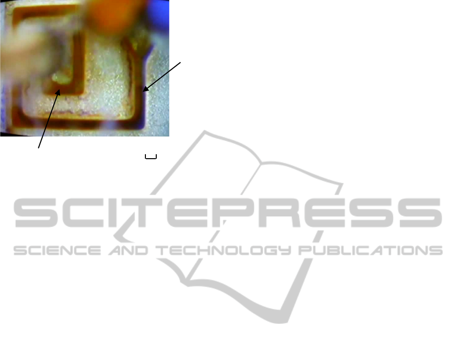
use of micro-fluidic paths were formed. An example
of micro-mixer pattern is shown in Fig. 10. The
sizes of the devices were 14.3 mm × 5.7 mm, and
the favourable exposure dose was 3.5-4 J/cm
2
. The
designed widths of the Y-shape patterns at both
entrances and the repeatedly winding parts were 50
and 100 μm, respectively. The widths were
measured using the optional function prepared for
the scanning electron microscope (JSM 5510, JEOL).
Measured pattern widths were almost homogeneous,
as shown in Fig. 11. The diameters of two inlet ports
and an outlet port are 2mm.
Figure 10: Flow-path patterns with perpendicular
sidewalls.
Figure 11: Width homogeneity of flow-path patterns.
4 ASSEMBLY OF
MICRO-MIXERS
Micro-mixers were assembled using the resist
micro-fluidic paths formed on silicon wafers. Plastic
vessels and lids were fabricated using a simple 3
dimensional milling machine. A silicon wafer chip
with the resist paths was embedded in a concave
made on the vessel, and the resist surface was
slightly stuck out from the top surface of the vessel,
as shown in Fig. 12. As a result, the resist surface
was homogeneously pressed by the flat lid. Each of
the thickness of the vessel and the lid was as large as
1mm
0
20
40
60
80
100
120
140
0 20406080100
Measurement point number
Width of trench
p
attern
(
μ
m
)
BIODEVICES2014-InternationalConferenceonBiomedicalElectronicsandDevices
8

5 mm so as not to be bent and curved when they
were bound by bolts and nuts. Micro-tubes with
inner and outer diameters of 1 and 2 mm were
attached to the inlets and outlet using epoxy
adhesive. No heat treatments were added to the resist
paths after the patterning.
Fig. 13 shows the outside view of the assembled
micro-mixer. The sizes of the device were 23×30×15
mm. The depth of the rectangular concave engraved
on the vessel surface was made a little shallower
than the total thickness of the micro-mixer chip. As
a result, the resist-path surface became higher than
the vessel surface. The height difference or stick-out
height h is almost equal to the gap between the
surface of vessel and the back surface of lid, as
shown in the figure. It was clarified that the stick-out
height h should be controlled between 35 and 45 μm
to prevent the leaks.
Wafer
Resist
Exposurelight
Mask
Lid
Vessel
①
Resist
②
Exposure
③
Development
④
Assemble
h
Figure 12: Fabrication method of micro-mixer.
5 FLOW TEST
Two coloured liquids were simultaneously injected
from the Y-shape inlets for verifying that they did
not leak out though the sealed gaps between the
surfaces of resist patterns and the lid plate. The
liquids were injected using manual syringes at the
initial stage, and automatic syringe pumps at the
final stage. Coloured waters were used as the liquids.
Because the seal depends on the elastic deformation
Figure 13: Outside View of the fabricated micro-mixer
Yellowwater
Bluewater
Figure 14: Non-mixing flow of two coloured waters.
Blue and yellow waters flew without being mixed.
of the resist, it was necessary that the surface of the
resist film was sufficiently stuck out from the vessel
surface, as mentioned above. On the other hand, the
lid plate is bended when it is bound with the vessel
at the four corners, and the bending deformation
increase depending on the stick-out height of the
resist. For this reason, the optimum stick-out height
should be decided considering the rigidity or
thicknesses of the lid and the vessel.
Fig. 14 shows the flow in the mixer. When same
liquids with yellow and blue colours were
simultaneously injected, the two liquids were
separately flown without being mixed together.
In the past research, two liquids prepared
10 mm
FabricationofPreciseMicro-fluidicDevicesusingaLow-costandSimpleContact-exposureToolforLithography
9
100µm
Separated
Mixed
Figure 15: Example of micro-mixing.
similarly were successfully mixed in a snail-shape
channel, as shown in Fig. 15. In this case, liquids
coloured in red and blue were used. Separated red
and blue flows were gradually mixed after they
passed corners. Accordingly, it is thought that the
liquids will be mixed if the shape of the channel is
improved. A lot of papers had been written on
micro-mixing in micro-fluidic devices (Jain, et al.,
2013) (Rahimi, M., et al., 2014). Considering the
reported remarks, vigorous research efforts should
be done hereafter.
6 CONCLUSIONS
A very simple and low-cost exposure tool was
developed, and applied to fabricate micro-fluidic
devices in which resist patterns were directly used as
flow paths. In spite of using such a simple and low-
cost tool, precise flow-paths with perpendicular
sidewalls were successfully fabricated, because a
blue filter was inserted to adjust the light absorption
of the thick resist film. Micro-fluidic device chips
made by the resist were embedded in the plastic
vessels, and capped by the lids. Although the lids
were simply bound with the vessels using small
bolts and nuts, injected fluids were flown without
leaks. The developed tool and the method to
fabricate micro-fluidic devices will be effective and
useful for economical small-volume production.
ACKNOWLEDGEMENTS
This work was partially supported by Research
Institute for Science and Technology of Tokyo
Denki University, Grant Number Q13T-02.
REFERENCES
Avram, M., Iliescu, C., Volmer, M., Avram, A., 2008.
Microfluidic device for magnetic separation in lab-on-
a-chip systems, Digest of Papers, Microprocesses and
Nanotechnology 2008, 21
st
International
Microprocesses and Nanotechnology Conference,
442-443.
Bouhadda, I., Sagazan, O., Bihan, F. L., 2012. Suspended
Gate Field Effect Transistor with an Integrated Micro-
Fluidic Channel Performed by Surface
Micromachining for Liquids Sensing, Procedia
Engineering 47, 754-757.
Campbel, K., McGrath, T., Sjölander, S., Hanson, T.,
Tidare, M., Jansson, Ö., Moberg, A., Mooney, M.,
Elliott, C., Buijs, J., 2011. Use of a novel micro-fluidic
device to create arrays for multiplex analysis of large
and small molecular weight compounds by surface
plasmon resonance, Biosensors and Bioelectronics 26,
3029-3036.
Chen, C. S., Chen, S. C., Liao, W. H., Chien, R. D., Lin, S.
H., 2010. Micro injection molding of a micro-fluidic
platform, International Communications in Heart and
Mass Transfer 37, 1290-1294.Jacobs, T., Kutzner, C.
Kropp, M., Brokmann, G., Lang, W., Steinke, A.,
Kienke, A., Hauptmann, P., 2009. Combination of a
novel perforated thermoelectric flow and impedimetric
sensor for monitoring chemical conversion in micro
fluidic channels, Procedia Chemistry 1, 1127-1130.
Curto, V. F., Fay, C., Coyle, S., Byrne, R., O’Toole, C.,
Barry, C., Hughes, S., Moyna, N., Diamond, D.,
Lopez, F. B., 2012. Real-time sweat pH monitoring
based on a wearable chemical barcode micro-fluidic
platform incorporating ionic liquids, Sensors and
Actuators B 171-172, 1327-1334.
Eun, D. S., Kong, D. Y., Chang, S. J., Yoo, J. H., Hong, Y.
M., Shin, J. K., Lee, J. H., 2008. Micro-PCR Chip
with Nanofluidic Heat-Sink for Faster Temperature
Changes, Digest of Papers, Microprocesses and
Nanotechnology 2008, 21
st
International
Microprocesses and Nanotechnology Conference ,
448-449.
Horiuchi, T., Watanabe, H., Hayashi, N., Kitamura, T.,
2010. Simply Fabricated Precise microfluidic Mixer
with Resist Flow Paths Sealed by an Acrylic Lid,
Proceedings of The third International Conference on
Biomedical Electronics and Devices, 82-87.
Jain, M., Nandakumar, K., 2013. Optimal patterning of
heterogeneous surface charge for improved
electrokinetic micromixing, Computers and Chemical
Engineering 49, 18-24.
Kashkary, L., Kemp, C., Shaw, K. J., Greenway, G. M.,
Haswell, S. J., 2012. Improved DNA extraction
efficiency from low level cell numbers using a silica
monolith based micro fluidic device, Analytica
BIODEVICES2014-InternationalConferenceonBiomedicalElectronicsandDevices
10

Chimica Acta 750, 127-131.
Liu, F., Tan, K. B., Malar, T. P., Bikkarolla, S. K., Kan, J.
A., 2013. Fabrication of nickel molds using proton
beam writing for micro/nano fluidic devices,
Microelectronic Engineering 102, 36-39.
Lopez, F. B., Scarmagnani, S., Walsh, Z., Paull, B., Macka,
M., Diamond, D., 2009. Spiropyran modified micro-
fluidic chip channel as photonically controlled self-
indicating system for metal ion accumulation and
release, Sensors and Actuators B 140, 295-303.
Martinez, A. W., Phillips, S. T., Wiley, B. J., Gupta, M.,
Whiteside, G. M., 2008. Flash: A rapid method for
prototyping paper-based microfluidic devise, Lab Chip
8, 2146-2150.
Martinez, A. W., Phillips, S. T., Whiteside, G. M.,
Carrilho, E., 2010. Diagnostics for the developing
world: microfluidic paper-based analytical devices,
Anal. Chem. 82, 3-10.
Oakley, J. A., Robinson, S., Dyer, C. E., Greenman, J.,
Greenway, G. M., Haswell, S. J., 2009. Development
of a gel-to-gel electro-kinetic pinched injection
method for an integrated micro-fluidic based DNA
analyser, Analytica Chimica Acta 652, 239-244.
Rahimi, M., Azimi, N., Parvian, F., Alsairafi, A. A., 2014.
Computational Fluid Dynamics modelling of
micromixing performance in presence of
microparticles in a tubular sonoreactor, Computer and
Chemical Engineering 60, 403-412.
Riahi, M., 2012. Fabrication of a passive 3D mixer using
CO2 laser ablation of PMMA and PDMS moldings,
Microchemical Journal 100, 14-20.
Serra, N., Maeder, T., Gentsch, O., Ryser, P., 2011.
Fabrication of polymer-based micro devices:
Formulation study of the paste, Sensors and Actuators
A 172, 336-340.
Yang, R., Lu, B. R., Wang, J., Xie, S. Q., Chen, Y., Huq,
E., Q, X. P., Liu, R., 2009. Fabrication of micro/nano
fluidic channels by nanoimprint lithography and
bonding using SU-8, Microelectronic Engineering 86,
1379-1381.
FabricationofPreciseMicro-fluidicDevicesusingaLow-costandSimpleContact-exposureToolforLithography
11
