
Analytical Model of SSD Parallelism
Jinsoo Yoo
1
, Youjip Won
1
, Sooyong Kang
1
, Jongmoo Choi
2
, Sungroh Yoon
3
and Jaehyuk Cha
1
1
Department of Computer and Software, Hanyang University, Seoul, Korea
2
Dankook University, Yongin, Korea
3
Seoul National University, Seoul, Korea
Keywords:
Flash, SSD, Parallelism, Simulation, Modeling.
Abstract:
SSDs support various IO parallel mechanisms such as channel parallelism, way parallelism, and plane par-
allelism to increase IO performance. To measure an SSD’s performance in a simulation environment, the
simulator has to support the parallel IO operations of an SSD by modeling its internal IO behaviors. In this pa-
per, we developed an analytical model to calculate the IO latency of multi-channel and multi-way architected
SSDs. In formulating the IO latency model, we categorized SSDs’ IO types into two operations: single page
read/write operations and multiple page read/write operations. With the IO latency model, we can calculate
the IO performance of a real SSD, Intel X25-M, with a 3.8% offset.
1 INTRODUCTION
NAND flash based storage, such as an SSD, made its
way to main storage device in all types of comput-
ing devices, e.g., smartphones, TVs, PCs, and servers
(Wong, 2013). An SSD is a complex device consist-
ing of flash chips, micro-controller, e.g., ARM, mem-
ory, which is DRAM or SRAM, and host interface,
e.g., SATA or PCIe. The software component of an
SSD is called Flash Translation Layer (FTL). It is
responsible for (i) translating a logical address into
physical address, (ii) evenly distributing the wear-
outs, and (iii) consolidating the invalid pages. In de-
signing an SSD, it is very important that all design
parameters, e.g., the number of channels, the number
of ways, physical page size, address translation algo-
rithms, garbage collection algorithms, etc., are deter-
mined, properly incorporating the interactions among
these components and the SSDs’ workload character-
istics (or target usage).
There exist a number of approaches in predict-
ing the behavior of an SSD under various design pa-
rameters: analytical formulation (Desnoyers, 2012),
trace driven simulation (Agrawal et al., 2008), (Kim
et al., 2009), (Cho et al., 2012), virtual machine based
simulation (Yoo et al., 2013), and FPGA based pro-
totyping (OpenSSD, 2011), (Lee et al., 2010). An-
alytical formulation (Desnoyers, 2012) is most flex-
ible, but it is the least accurate way of predicting
the performance of an SSD. FPGA based prototyp-
ing (OpenSSD, 2011) (Lee et al., 2010) is the most
expensive and inflexible way of predicting the perfor-
mance. However, it enables users to closely examine
the real time behavior of a given FTL algorithm and
its performance implications.
Virtual machine based simulation (Yoo et al.,
2013) provides the benefits of both methods. The
hardware configurations, e.g., the number of chan-
nels/ways and DRAM size, and software algorithms,
e.g., address mapping and garbage collection algo-
rithm, can be changed in a versatile manner. It also
enables users to examine the host performance with
reasonable accuracy. VSSIM emulates the real time
performance of an SSD (X-25M) within a 5% error
rate (Yoo et al., 2013).
A key technical ingredient is how to introduce the
proper I/O latency in an “algorithmic way. An SSD
consists of a number of physical components, e.g.,
NAND chips, bus, micro-controllers. These compo-
nents work independently (or in a synchronized man-
ner) which yields multiple concurrent activities in the
device. A latency of an I/O request is governed by
the concurrent processing of this I/O request among
a number of SSD components. This work focuses on
developing an efficient way of modeling the concur-
rent behavior of SSD components. Instead of emu-
lating the individual components, e.g., NAND flash
chips, as a thread, we developed an elaborate delay
model to compute the latency for a given IO com-
mand. The proposed delay model enables us to emu-
551
Yoo J., Won Y., Kang S., Choi J., Yoon S. and Cha J..
Analytical Model of SSD Parallelism.
DOI: 10.5220/0005011605510559
In Proceedings of the 4th International Conference on Simulation and Modeling Methodologies, Technologies and Applications (SIMULTECH-2014),
pages 551-559
ISBN: 978-989-758-038-3
Copyright
c
2014 SCITEPRESS (Science and Technology Publications, Lda.)

late the parallel behaviors of SSD components with-
out modeling each component with a thread.
By allocating a thread to each individual compo-
nent, we can easily model the concurrent behaviors
and their interactions with other SSD components.
However, the lock contentions and the context switch
overheads can become significant and can negatively
affect the emulator accuracy. For example, to emulate
Intel X25-M SSD (Intel, 2009), which has 10 chan-
nels and 2 ways, there can be as many as 30 threads
to model 20 flash planes and 10 channels of X25-M.
In this work, we developed an analytical model
that calculates IO delays in multi-channel/multi-way
SSDs. The proposed delay model precisely computes
the latency of a read (or write) request which is ser-
viced by multiple NAND flash chips across the chan-
nels and ways. This model enables an emulator to
emulate the parallel behavior of SSD components us-
ing a single thread. For example, when receiving an
IO request, the thread calculates IO latency with our
latency model and imposes a proper amount of delay
using busy waiting method. This way, a single thread
IO emulator can be implemented without a multi-
threaded method. When we compared the result of
our IO latency model with a real SSD, Intel X25-M,
the IO latency model showed less than a 3.8% error
rate.
2 BACKGROUND
I/O Buffer
DRAM
Enqueue
Dequeue
Data
Command
Channel 0 Channel 1
Channel 3
NAND
Flash
NAND
Flash
NAND
Flash
NAND
Flash
NAND
Flash
NAND
Flash
NAND
Flash
NAND
Flash
Channel 2
Host Interface (SATA, PCIe)
Flash
Memories
%QOOCPFSWGWG
CPU
Firmware
(NCUJEQPVTQNNGT
Figure 1: Organization of an SSD (4 channels, 2 ways).
Figure 1 shows the internal block diagram of an SSD
with 4 channels and 2 ways. Through host interface
(SATA, PCIe, etc.), the SSD receives IO commands
which include the starting sector number (512Byte
per a sector) and the sector length. The IO request
from the host is enqueued in the command queue and
the accompanying data is stored in the device buffer.
This device buffer is often called the write buffer
(Kim and Ahn, 2008). The firmware of the SSD lo-
cates the NAND flash blocks to where the incoming
IO request is directed and issues an IO command to
the respective NAND controllers.
Block 0
Block 4094
ㄾ
Page Register
Block 1
Block 4095
ㄾ
Page Register
Block 4096
Block 8190
ㄾ
Page Register
Block 4097
Block 8191
ㄾ
Page Register
Block 2
Block 3 Block 4098 Block 4099
Page 0
Page 1
ㄾ
Page n
Page 0
Page 1
ㄾ
Page n
Page 0
Page 1
ㄾ
Page n
Page 0
Page 1
ㄾ
Page n
Plane 0 Plane 1 Plane 2 Plane 3
Figure 2: Internal Architecture of NAND Flash Memory
(Samsung, 2006).
Flash Memory Read and Write: Figure 2 shows the
internal architecture of Samsung NAND flash mem-
ory (Samsung, 2006). Flash memory consists of mul-
tiple pages and each page is 2 ∼ 8KByte in size. Flash
memory conducts erase operations in units called a
block which consists of multiple pages. The set of
blocks that use the same register to transfer data is
called a plane. In a write operation, flash controller
writes data to a register. After the register write is
done, the data in the register is programmed in a free
page in flash memory. Read operations are processed
in the opposite direction of write operations. In a read
operation, flash memory reads data from a flash page
and writes it to a register. When it is completed, the
flash controller takes the data through a channel.
SSDs exploit various levels of IO parallelism,
such as plane parallelism, channel parallelism, and
way parallelism, to boost up the I/O performance and
to hide latency of flash write and read operations.
Reg Write Cell Programming
Cell ProgrammingIdle
Idle
PLANE 0
PLANE 1
time
Reg Write
Figure 3: Plane Parallelism Timing Diagram.
Plane Parallelism: The internal IO behavior of flash
memory can be implemented in parallel by using mul-
tiple registers at the same time. In Figure 2, flash
memory can process 2-page IOs in parallel. After
sending data to a register in Plane 0, the flash con-
troller transfers second data to a register in Plane 1.
As the registers share the same channel, the flash con-
troller cannot access the two registers at the same
time. After each data transfer from the flash controller
to a register is completed, each plane starts program-
ming the data in a free page in each plane. Since the
data transfer time between the flash controller and a
register (82usec for Samsung NAND flash (Samsung,
2006)) is much shorter than the programming time
SIMULTECH2014-4thInternationalConferenceonSimulationandModelingMethodologies,Technologiesand
Applications
552

of the flash page (900usec for Samsung NAND flash
(Samsung, 2006)), the two-page programming opera-
tion can be conducted in parallel. This is called ‘plane
parallelism’. Figure 3 shows the timing diagram of
plane parallelism. Plane parallelism can also be used
for read operations.
Channel 0
Flash 0
Page A
Flash 2
Channel 1
Flash 1
Page B
Flash 3
Flash controller
(a) Channel Parallelism
Channel 0
Flash 0
Page A
Flash 2
Page B
Channel 1
Flash 1
Flash 3
Flash controller
(b) Way Parallelism
Figure 4: Channel and Way Parallelism of an SSD .
Reg Write Cell Programming
Cell Programming
Flash 0
Flash 1
time
Reg WriteCh
Idle
Figure 5: Channel Parallelism Timing Diagram.
Channel Parallelism: Using several channels, the
flash controller concurrently processes multiple IOs.
This is called ‘channel parallelism’. For example,
Figure 4(a) shows the connection between flash mem-
ories and the flash controller in 2 channels, 2 ways
SSD. Because Flash 0 and Flash 1 are used by differ-
ent channels, Page A and Page B can each be written
in different flash memories using channel parallelism.
The timing diagram of the 2-page write operation is
shown in Figure 5. Before the flash controller writes
data to Flash 1, channel switching delay, denoted as
Ch, occurs. Because channel switching delay is suf-
ficiently short (33usec (Yoo et al., 2011)), the flash
controller can write the pages to each flash memory
at about the same time.
Reg Write Cell Programming
Cell Programming
Flash 0
Flash 2
time
Reg WriteWayIdle
Idle
Figure 6: Way Parallelism Timing Diagram.
Way Parallelism: Flash memories in the same chan-
nel can process IOs in parallel. This is called ‘way
parallelism’. In Figure 4(b), the flash controller can
utilize way parallelism using Flash 0 and 2 in Channel
0. Because the flash memories share the same chan-
nel, a flash memory in the channel can transfer data
with flash controller only if the channel is not occu-
pied by another flash memory operation. The timing
diagram of way parallelism is shown in Figure 6. As
both Flash 0 and Flash 2 use Channel 0, the flash con-
troller can implement Page B operation after the end
of the register write operation of Page A. Before the
start of Page B operation, way switching delay(Way)
occurs because Flash 0 and Flash 2 are connected to
different ways. After way switching delay, the flash
controller transfers Page B data to Flash 2 and then
Flash 2 starts page write operation.
By using these kinds of IO parallel methods, SSDs
achieve higher IO bandwidth.
3 MODELING THE LATENCY
In this section, we developed IO latency models for
SSDs that are structured multi channels and multi
ways. When developing an IO latency model, we
haveto consider concurrent IO processing of the SSD.
First, we describe the single page IO latency model.
Then, we expand the model to the multiple page IO
latency model. We define the term IO latency as the
time interval between the arrival of the IO command
from the host to the device and the time when the I/O
device sends the IO interrupt notifying the completion
of an IO command. Terms used in each IO latency
model are listed in Table 1.
3.1 Modeling Single Page Write/Read
For a write operation, IO latency varies widely de-
pending on when the device sends completion inter-
rupt. The device can send completion interrupt ei-
ther when the incoming data is written at device write
buffer or when data is stored at NAND flash. In the
former case, the write latency is governed by the in-
terface speed and the amount of data to be written.
In this work, we focus on the latter case, when the
host requests the data to be written to the storage me-
dia, e.g., with “O
DIRECT option”. From the defini-
tion, single page write latency of an SSD can be rep-
resented by Eq. 1. That is, the total page write time
(W
page
) is a summation of 3 processing times: chan-
nel switching delay(W
ch
), data transfer delay between
a flash controller and a flash memory register(W
reg
),
and data programming delay in a free page in a flash
memory (W
cell
).
W
page
= W
ch
+W
reg
+W
cell
(1)
We also define the read latency as the time from
the arrival of the read command to the SSD to the
time when the SSD sends the IO completion inter-
rupt to the host. Then, using Eq. 1, we can get the
single read latency model as Eq. 2. Single page read
AnalyticalModelofSSDParallelism
553
Represent Description Represent Description
S
page
Page size N
plane
The number of planes per flash
W
ch
/ R
ch
Channel switching delay for write / read ρ The maximum number of IOs per cycle
W
reg
/ R
reg
Register write / read delay S
file
File size
W
cell
/ R
cell
NAND write / read delay S
record
Record size
W
page
/ R
page
1 Page write / read delay N
page
The number of pages per record
N
ch
The number of channels N
cycle
The number of cycles per record
N
way
The number of ways N
remain
The number of IOs in the last IO cycle
Table 1: Parameters in the SSD IO Performance Modeling.
latency(R
page
) is the aggregation of channel switching
delay(R
ch
), NAND page read delay(R
cell
), and regis-
ter read delay(R
reg
).
R
page
= R
ch
+ R
reg
+ R
cell
(2)
3.2 Write Operations
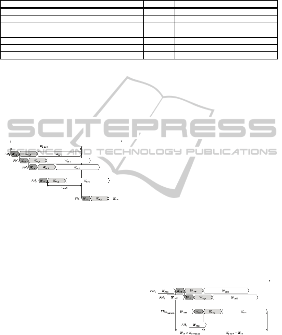
ㄾ
Cycle 1
Cycle 2
time
Figure 7: Sequential Write Timing Diagram.
A host request can include more than a one page I/O
request. For example, when a 512KByte SATA write
command is received, an SSD with 4KByte page
size operates 128 page writes. When multiple page
write requests are received, a multi-channel/multi-
way structured SSD concurrently processes the oper-
ations by utilizing IO parallelism. Figure 7 illustrates
a timing diagram of each flash memory behavior in
processing multiple page write requests.
When an SSD uses channel parallelism, way par-
allelism, and plane parallelism, we denote the maxi-
mum number of pages that can be processed in par-
allel at the same time as ρ. In other words, an SSD
can process ρ page writes in a one cycle. In each
cycle, a flash memory which deals with 1 ∼ ρ page
IOs is denoted as FM
1
∼ FM
ρ
. First, the flash con-
troller sends a page write request to FM
1
and channel
switching delay W
ch
is imposed. After that, a regis-
ter write delay (W
reg
) occurs followed by NAND page
write delay (W
cell
). The summation of these opera-
tion times is a one page write time of the SSD and is
denoted as W
page
. After channel switching delay for
FM
1
has occurred, the flash controller writes data to
the register in FM
1
while sending another page write
request to FM
2
. Before data is written to FM
2
, chan-
nel switching delay also occurs. This is because FM
1
and FM
2
are used in different channels. In the same
way, after channel switching delay for FM
2
has oc-
curred, the flash controller sends another page write
request to the next flash memory. The flash controller
repeats this process until it sends a page write request
to FM
ρ
. Figure 7 shows the start of the second cycle
after the first cycle is done. To start the first write op-
eration of second cycle at FM
1
, the write operation of
FM
1
should be completed. The waiting time of the
second cycle before starting the first page write op-
eration is denoted as t
wait
which is formulated as Eq.
3.
t
wait
=
W
page
−W
ch
× ρ if W
page
> W
ch
× ρ
0 otherwise
(3)
If the single page writing time(W
page
) is suffi-
ciently short, ‘t
wait
’ becomes 0 and the second cycle
can start its first page write operation without waiting.
The processing time for a cycle is the time from
the start of first page write of a cycle to the start of
first page write of the next cycle. It is denoted as t
cycle
and can be calculated as Eq. 4.
t
cycle
= W
ch
× ρ+ t
wait
(4)
ㄾ
Cycle n
time
ㄾ
Figure 8: Sequential Write Timing Diagram (2).
Timing diagram of the last cycle n is shown in Fig-
ure 8. In some cases, the number of IOs conducted in
the last cycle can be less than ρ and then is denoted as
N
remain
. From Figure 8, we can easily get the process-
ing time of the last cycle as follows:
SIMULTECH2014-4thInternationalConferenceonSimulationandModelingMethodologies,Technologiesand
Applications
554
t
cycle
last
= W
ch
× (N
remain
− 1) +W
page
(5)
Using Eq. 5, we can calculate t
record
, which repre-
sents the processing time of a host write request. For
a write request, the number of cycles that an SSD has
to repeat is denoted as N
cycle
. Then, t
record
is calcu-
lated as follows:
t
record
= t
cycle
× (N
cycle
− 1) +t
cycle
last
= (W
ch
× ρ+ t
wait
) × (N
cycle
− 1)
+W
ch
× (N
remain
− 1) +W
page
= W
ch
× (ρ× (N
cycle
− 1) + N
remain
− 1)
+t
wait
× (N
cycle
− 1) +W
page
Because ‘ρ × (N
cycle
− 1) + N
remain
’ equals the to-
tal number of pages in a record, N
page
, we can get the
write latency model, t
record
, as follows:
t
record
= W
ch
× (N
page
− 1) + t
wait
× (N
cycle
− 1) +W
page
(6)
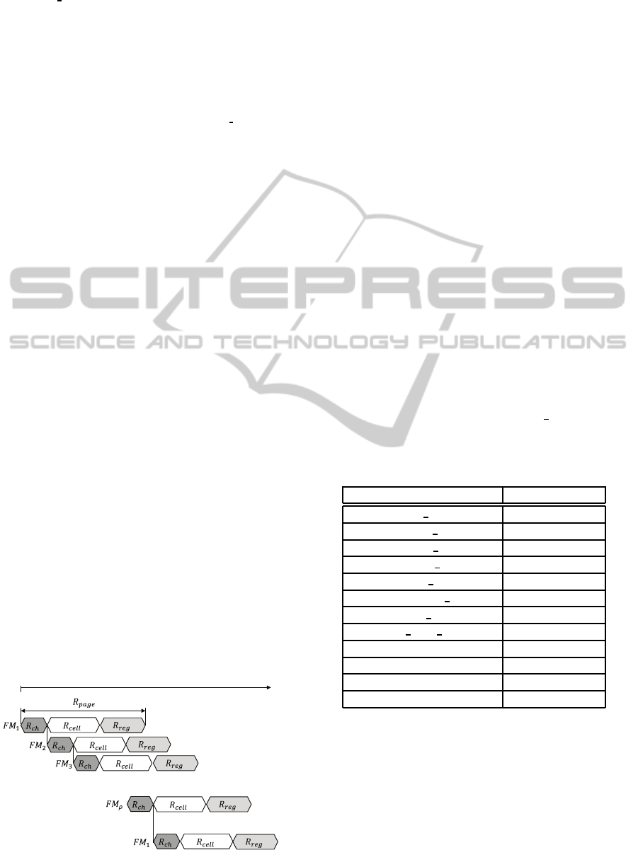
3.3 Read Operations
We can define the read latency model as the same way
we did for the write latency model. Using Eq. 6, the
read latency model can be formulated as Eq. 7.
t
record
= R
ch
× (N
page
− 1) + t
wait
× (N
cycle
− 1) + R
page (7)
In some cases, Eq. 7 can be further simplified.
Figure 9 shows such a case. An important feature in
this case is that there is no waiting time (t
wait
) when
a cycle changes. This results from the NAND read
operation being much faster than the NAND write
operation (50usec for a read operation vs. 900usec
for a write operation in Samsung NAND flash (Sam-
sung, 2006)). In this case, ‘t
wait
’ in Eq. 7 becomes 0
and the read latency model is simplified as ‘t
record
=
R
ch
× (N
page
− 1) + R
page
’.
ㄾ
Cycle 1
Cycle 2
time
Figure 9: Sequential Read Timing Diagram.
4 EXPERIMENT
In this section, we validate the accuracy of the IO la-
tency models with a real SSD, Intel X25-M. Using
analytical models, we calculated the IO performance
of an SSD that is configured the same way as X25-M
under various workloads. Then, we measured the IO
performance of X25-M performing the same work-
loads and compared both results. Next, we compared
the theoretical performance with VSSIM SSD simu-
lator (Yoo et al., 2013). From this experiment, we are
assured that the IO latency models can be used in VS-
SIM as an IO emulator module.
4.1 Validation with X25-M
To validate the single page IO latency model (Eq. 1,
Eq.2) and write/read latency model (Eq. 6, Eq. 7),
we compared the theoretical performance from the la-
tency models with the measured performance of X25-
M. Table 2 shows the SSD configurations of X25-M.
The performance of the NAND flash memory used in
X25-M is described in Table 3. For X25-M, chan-
nel switching delay for read operation is 16usec (Yoo
et al., 2011) and channel switching delay for write op-
eration is 33usec (Yoo et al., 2011). When writing or
reading data with X25-M, we used O
DIRECT op-
tion and opened X25-M as a raw device to minimize
the filesystem interference and to measure the NAND
page write/read IO latency of the SSD.
Parameter Value
PAGE SIZE 4 KByte
SECTOR SIZE 512 Byte
FLASH NB 20
BLOCK NB 4096 blocks
PAGE NB 256 pages
CHANNEL NB 10
WAY NB 2
PLANE PER FLASH 2
Sequential Read 250 MByte/sec
Sequential Write 70 MByte/sec
Sequential 4KByte Read 35,000 IOPS
Sequential 4KByte Write 6,600 IOPS
Table 2: Intel X25-M SSD Specifications.
We compared the result of single page write/read
latency model with the IO performance of X25-M.
The workload consisted of writing (or reading) a
512MByte file with page size in a random offset. For
calculating single page IO performance, we used Eq.
1 for single page write latency and Eq. 2 for sin-
gle page read latency. In calculating analytical per-
formance, we adjusted NAND programming delay
AnalyticalModelofSSDParallelism
555
REG WRITE DELAY 82 usec
REG READ DELAY 82 usec
CELL PROGRAM DELAY 900 usec
CELL READ DELAY 50 usec
BLOCK ERASE DELAY 2000 usec
Table 3: NAND Flash Memory Specifications Used in Intel
X25-M (29F32G08CAMC1).
(W
cell
, 900usec) and NAND read delay (R
cell
, 50usec)
to 940usec and 140usec, respectively, to account for
the performance degrade of X25-M used in the exper-
iment which become worn out by intensive IO tests
(Dijkstra, 1982). Table 4 shows the theoretical per-
formance of the single page IO latency model and the
measured performance of X25-M. The error rates of
single page latency model were 0.5% and 1.0% for
write and read operations, respectively.
Workload Delay Model X25-M Error
Write 947.9 IOPS 944.6 IOPS 0.5%
Read 4201.7 IOPS 4158.0 IOPS 1.0%
Table 4: Single Page Write/Read Latency Model Validation
with X25-M (Filesize 512MByte, Record size 4KByte, raw
device, O
DIRECT).
Using write workloads that cause multiple page
write requests, we validated the accuracy of the write
latency model (Eq. 6). The workloads consisted
of writing a 512MByte file sequentially with record
sizes of 512KByte, 256KByte, 128KByte, 64KByte,
32KByte, 16KByte, 8KByte, and 4KByte. In Eq. 6,
we adjusted NAND programming delay, W
cell
, from
900usec to 940usec to account for the wear level of
the actual X25-M used in the experiment. Figure
10 shows the performances based on the write la-
tency model versus actual X25-M. The predicted re-
sults from our model differed from the actual results
by 4%.
The read latency model showed more accurate
results than the write latency model. To validate
the read latency model, 8 sequential read work-
loads were performed: the workloads consisted of
reading a 512Mbyte file sequentially with record
sizes of 512KByte, 256KByte, 128KByte, 64KByte,
32KByte, 16KByte, 8KByte, and 4KByte. In cal-
culating the theoretical performance with Eq. 7, we
adjusted NAND read delay, R
cell
, from 50usec to
140usec to account for the performance degrade level
of the actual X25-M used in the experiment. Figure
11 shows the results. For sequential read workloads,
the difference between our models calculations and
the actual results were within 1.3%.
From the validation results with X25-M, we con-
0
10
20
30
40
50
60
4 8 16 32 64 128 256 512
Bandwidth(MB/s)
Record Size(KByte)
Intel X25-M
Write Latency Model
Figure 10: Write Latency Model Validation with X25-M
(Filesize 512MByte, raw device, O
DIRECT).
0
30
60
90
120
150
180
210
4 8 16 32 64 128 256 512
Bandwidth(MB/s)
Record Size(KByte)
Intel X25-M
Write Latency Model
Figure 11: Read Latency Model Validation with X25-M
(Filesize 512MByte, raw device, O
DIRECT).
firmed that the read/write latency models precisely
describe the parallel IO processing of an SSD.
4.2 Validation with VSSIM
We compared the IO performance from IO latency
models with that from VSSIM SSD Simulator (Yoo
et al., 2013) using the same SSD configurations.
Thereby, we confirmed that our IO latency model can
be used as an IO emulator in an SSD simulator. VS-
SIM is a virtual machine based SSD simulator which
can measure the host performance operating on top
of the simulator. With VSSIM, a user can specify a
virtual SSD which processes IO requests based on its
configurations.
IO Emulator Module
(IO Latency )
FTL Module
SSD Monitor
page read/write
erase
Performance Information
read/write
SSD Module
IO Information
SATA Command from Host
QEMU
Figure 12: VSSIM SSD Module Architecture.
VSSIM consists of QEMU, SSD module, and
RAMDISK. A guest OS installed on QEMU regards
the RAMDISK allocated in main memory as an SSD.
The architecture of VSSIM SSD module is shown in
Figure 12. SSD module is composed of FTL module,
IO emulator module, and SSD monitor. FTL module
SIMULTECH2014-4thInternationalConferenceonSimulationandModelingMethodologies,Technologiesand
Applications
556
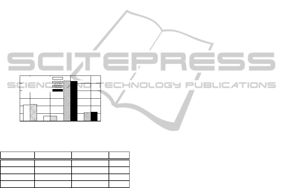
maintains mapping information between logical page
address and physical page address. IO emulator man-
ages IO behavior of SSDs by generating IO latency.
SSD monitor shows the SSD performance informa-
tion to users by graphic user interface.
For validating IO latency models with VSSIM,
we used 4 workloads: sequential write/read and ran-
dom write/read. For sequential IO workloads, we
wrote and read a 512Mbyte file sequentially with a
512Kbyte record size. For random IO workloads, we
wrote and read a 512Mbyte file in random offset with
a 4KByte page size. The virtual SSD in VSSIM was
configured the same way as X25-M specifications.
The same configurations were also used in IO latency
models. Linux guest OS is installed on VSSIM and
the IO performance is checked on the Linux. The
performance results from VSSIM and the IO latency
models on the 4 workloads are shown in Figure 13
and Table 5.
0
100
200
300
400
500
Seq Read
Seq Write
Rand Read
Rand Write
0
1000
2000
3000
4000
Bandwidth(MB/s)
IOPS
VSSIM (Seq)
IO Model (Seq)
VSSIM (Rand)
IO Model (Rand)
Figure 13: IO Latency Model Validation with VSSIM.
VSSIM IO Model Error
Seq Read 211.9 MB/s 220.3 MB/s 4.0 %
Seq Write 67.3 MB/s 65.7 MB/s 2.4 %
Rand Read 4235.1 IOPS 4201.7 IOPS 0.8 %
Rand Write 880.6 IOPS 947.9 IOPS 7.6 %
Table 5: IO Latency Model Validation with VSSIM.
Compared with VSSIM, the IO latency models
showed sequential read and write performances with
4.0% and 2.4% offset, respectively, and random read
and write performances with 0.8% and 7.6% offsets,
respectively. From the validation results, we con-
firmed that the IO latency models can be used in IO
emulator to impose proper amount of delay.
5 RELATED WORK
Analytic modeling of write performance (Desnoyers,
2012) provides block cleaning performance in terms
of the Write Amplification Factor (WAF): the ratio
between the number of page writes from the host to
the number of page writes that happen in an SSD. Al-
though this work provides a precise closed-form solu-
tion for the block cleaning performance for LRU and
greedy collection algorithm, it cannot be used to pre-
dict the IO latency of SSDs.
There has been much research on simulating the
performance of SSDs or flash memory. One of
the SSD simulators is NANDFlashSim (Jung et al.,
2012). NANDFlashSim simulates a single flash mem-
ory and can configure a page size, IO latency, the
number of dies in a flash memory, and the number
of planes. It supports various IO modes such as cache
mode, internal data move mode, multi-plane mode,
and interleaved mode. NANDFlashSim uses local
clock domain, and all flash memories are synchro-
nized with it. At every clock, NANDFlashSim checks
the progress of each flash memory and changes its
state. Because NANDFlashSim only simulates flash
memory, it cannot measure the performance of SSDs
using channel, way, and plane parallelism.
CPS-SIM (Lee et al., 2009) can simulate SSDs
that use channel parallelism. Similar to NANDFlash-
Sim, CPS-SIM is a clock-driven simulator, which
synchronizes its state machine with local clock. For
IO processing, each flash memory is managed by
a finite state machine. CPS-SIM checks each flash
memory for the completion of IOs and changes its
state. For higher accuracy of the simulation result,
clock-driven simulators have to use higher clock fre-
quency. At the same time, clock driven simulators
need enough clock intervals to check and change the
state of every flash memory. These conflicting needs
make it difficult for clock-driven simulators to guar-
antee the accuracy of their simulation results.
There are simulators that provide a virtual
flash device in a main memory, such as NAND-
Sim (NANDSim, 2008) and Flash Disk Simulator
(El Maghraoui et al., 2010). A host uses virtual de-
vices as a primitive flash memory or as a block de-
vice. This enables us to check the performance of
the host, which operates on top of the virtual de-
vices. However, the simulators only simulate a flash
memory. Thus, we cannot get IO performance of an
SSD, which utilizes multi-channel and multi-way par-
allelism. Flash-DBSim (Jin et al., 2009) also provides
a virtual flash device to upper layer. Flash-DBSim
creates a virtual flash disk in memory which is man-
aged by MTD (Memory Technology Device) module.
MTD Module supports interfaces for Flash Trans-
lation Layer (FTL) to manipulate the virtual flash
disk. Unlike NANDSim, Flash-DBSim uses a trace
as workload. Because Flash-DBSim only simulates
a flash memory, it cannot test various IO parallelism
supported in an SSD.
AnalyticalModelofSSDParallelism
557

Trace driven SSD simulator is also widely used
to examine the internal behavior of SSDs. DISKSim
SSD Extension (Agrawal et al., 2008) and Flashsim
(Kim et al., 2009) are developed to simulate an SSD
based on DiskSim (Bucy et al., 2008). With these
simulators, users can configure the number of flash
memories, the number of planes per flash memory, the
page read/write latency, a page size, a block size, etc.
However, these simulators calculate the SSD perfor-
mance without imposing IO processing delay, which
means that they cannot be used to observe the host IO
performance in real time.
6 CONCLUSION
In this work, we developed an analytical model that
calculates the IO latency of an SSD. For modeling, we
considered concurrent IO processing of an SSD, such
as channel parallelism, way parallelism, and plane
parallelism. We classified SSDs’ IO types into single
page read/write request or multiple page read/write
request and developed IO latency model for each IO
type. Compared with the performance of a real SSD,
Intel X25-M, the latency models showed less than a
4% error rate in various workloads. We also proved
that the IO latency models can be used in an SSD
simulator by validating their results with VSSIM. The
IO performances calculated by our analytical models
were close to the simulation results of VSSIM with
a 0.8% ∼ 7.6% offset. Using the IO latency models,
SSD simulators can calculate and impose the desired
amount of IO latency for an IO request. Thus, the
simulator can simulate the IO performance of multi-
channel and multi-way SSDs without using multi-
threaded methods.
ACKNOWLEDGEMENTS
MLC SSD: This work is sponsored by IT R&D pro-
gram MKE/KEIT. [No.10035202, Large Scale hyper-
MLC SSD Technology Development].
REFERENCES
Agrawal, N., Prabhakaran, V., Wobber, T., Davis, J. D.,
Manasse, M., and Panigrahy, R. (2008). Design trade-
offs for SSD performance. In Proc. of Annual Techni-
cal Conference(ATC), USENIX, pages 57–70, Boston,
Massachusetts, USA.
Bucy, J. S., Schindler, J., Schlosser, S. W., and Ganger,
G. R. (2008). The disksim simulation environment
version 4.0 reference manual (cmu-pdl-08-101). Par-
allel Data Laboratory.
Cho, S., Won, Y., Kang, S., Cha, J., Choi, J., and Yoon,
S. (2012). Influence of number of channels and ftl
on ssd power consumption. In Proc. of International
Conference of Electrical, Computer, Electronics and
Biomedical Engineering (ICECEBE), Bangkok, Thai-
land.
Desnoyers, P. (2012). Analytic modeling of ssd write per-
formance. In Proc. of the Annual International Sys-
tems and Storage Conference(SYSTOR), ACM, Haifa,
Israel.
Dijkstra, E. W. (1982). Stepwise program construction.
Springer.
El Maghraoui, K., Kandiraju, G., Jann, J., and Pattnaik,
P. (2010). Modeling and simulating flash based
solid-state disks for operating systems. In Proc. of
WOSP/SIPEW, pages 15–26, San Jose, California,
USA.
Intel, C. (2009). Intel x25-m sata solid-state drive.
Specification. http://download.intel.com/design/
flash/nand/mainstream/mainstream-sata-ssd-
datasheet.pdf.
Jin, P., Su, X., Li, Z., and Yue, L. (2009). A flexible sim-
ulation environment for flash-aware algorithms. In
Proc. of the Conference on Information and Knowl-
edge Management(CIKM), ACM, pages 2093–2094,
Hong Kong, China.
Jung, M., Wilson, E., Donofrio, D., Shalf, J., and Kandemir,
M. (2012). Nandflashsim: Intrinsic latency variation
aware nand flash memory system modeling and sim-
ulation at microarchitecture level. In Proc. of Mass
Storage Systems and Technologies(MSST), IEEE, Pa-
cific Grove, CA, USA.
Kim, H. and Ahn, S. (2008). BPLRU: A buffer management
scheme for improving random writes in flash storage.
In Proc. of the conference on File and Storage Tech-
nologies(FAST), USENIX, volume 8, pages 1–14, San
jose, CA, USA.
Kim, Y., Tauras, B., Gupta, A., and Urgaonkar, B. (2009).
Flashsim: A simulator for nand flash-based solid-state
drives. In Proc. of the International Conference on
Advances in System Simulation(SIMUL), IEEE, pages
125–131, Washington, DC, USA.
Lee, J., Byun, E., Park, H., Choi, J., Lee, D., and Noh,
S. H. (2009). CPS-SIM: configurable and accurate
clock precision solid state drive simulator. In Proc. of
the Symposium on Applied Computing (SAC), ACM,
pages 318–325, Honolulu, Hawaii, USA.
Lee, S., Fleming, K., Park, J., Ha, K., Caufield, A. M.,
Swanson, S., Arvind, and Kim, J. (2010). Bluessd:
An open platform for cross-layer experiments for
nand flash-based ssds. In Proc. of The Workshop
on Architectural Research Prototyping(WARP), Saint-
Malo, France.
NANDSim (2008). Memory Technology Device.
www.linux-mtd.infradead.org.
OpenSSD (2011). Project. http://www.openssd-project.org.
Samsung, E. (2006). 2g x 8 bit / 4g x 8 bit nand flash mem-
ory (k9xxg08uxm). Specification.
SIMULTECH2014-4thInternationalConferenceonSimulationandModelingMethodologies,Technologiesand
Applications
558

Wong, G. (2013). SSD market overview. In Proc. of Inside
Solid State Drives (SSDs), Springer, volume 37, pages
1–17.
Yoo, B., Won, Y., Cho, S., Kang, S., Choi, J., and Yoon, S.
(2011). SSD characterization: From energy consump-
tion’s perspective. In Proc. of HotStorage, USENIX,
Portland, OR, USA.
Yoo, J., Won, Y., Hwang, J., Kang, S., Choi, J., Yoon, S.,
and Cha, J. (2013). VSSIM: Virtual machine based
ssd simulator. In Proc. of Mass Storage Systems and
Technologies(MSST), IEEE, Long Beach, CA, USA.
AnalyticalModelofSSDParallelism
559
