
Tera
h
Using Resonant Tu
n
Tadao Nagatsuma,
M
Gradu
a
1
K
21 S
a
Keywords: Terahertz, communicati
o
Abstract: This paper presents a tra
n
as both a transmitter a
n
experiments have succes
s
an RTD receiver and a tr
a
1 INTRODUCTION
Recently, there has been an increa
s
application of terahertz (THz) wa
v
THz) to the ultrahigh-s
communications. In particular, t
h
frequencies above 275 GHz is o
attentions among radio scientist
s
b
ecause these frequency bands h
a
allocated to specific active servic
e
p
ossibility to employ extremely lar
g
ultra-broadband wireless commu
n
Ostmann and Nagatsuma, 2
0
Nagatsuma, 2011).
A 300-GHz band wireless link a
t
40 Gbit/s has been reported, in w
h
b
ased transmitter and a Schot
t
(SBD) detector are used (Nagats
u
To bring the THz wireless
technology to a widespread cons
u
the development of transmitters
b
semiconductor electronic devi
c
required. Among various semico
n
devices and integrated circuits, r
e
diodes (RTDs) have exhibited the
h
frequency at over 1 THz (Asada et
et al., 2010). In this paper, we
f
application of RTDs to receivers
communications. Sensitivity enh
a
strong nonlinearity of direct curr
e
voltage (I-V) characteristics is
h
ertz Wireless Communications
n
neling Diodes as Transmitters a
n
M
asayuki Fujita, Ai Kaku, Daiki Tsuji, and Shuns
u
a
te School of Engineering Science, Osaka University,
1
-3 Machikaneyma, Toyonaka 560-8531, Japan
nagatuma@ee.es.osaka-u.ac.jp
K
azuisao Tsuruda, and Toshikazu Mukai
Photonics R&D Center, Rohm Co., Ltd.,
a
iin Mizosaki-cho, Ukyo-ku, Kyoto 615-8585, Japan
o
n, resonant tunneling diode, transmitter, receiver, transceiv
e
n
sceiver module employing a resonant tunneling diode (RT
D
n
d a receiver just by changing the bias voltages. Error-f
r
s
fully been demonstrated at 300 GHz at bit rates of 10 Gbit
/
a
nsceiver, respectivel
y
.
s
ing interest in the
v
es (0.1 THz ~ 10
peed wireless
h
e use of carrier
ne of the strong
s
and engineers,
a
ve not yet been
e
s, and there is a
g
e bandwidths for
n
ications (Kleine-
0
11, Song and
t
a bit rate of over
h
ich a photonics-
t
ky-barrier diode
u
ma et al., 2013).
communications
u
mer marketplace,
b
ased on compact
c
es is urgently
n
ductor electronic
e
sonant tunneling
h
ighest oscillation
al., 2008, Suzuki
f
irst describe the
in THz wireless
a
ncement due to
e
nt (DC) current-
discussed both
theoretically and experiment
a
integrated with an MgO le
n
broadband o
p
eration at a bit
with a carrier frequency of 3
0
gigabit wireless transmissi
demonstrated using RTDs a
s
and receiver at 300 GHz.
Figure 1: Typical device layer str
u
2 DEVICE STRUC
T
OPERATION PR
I
Figure 1 shows a typical devi
c
RTD on InP substrate. The re
s
of the diode is composed of a
n
b
arrier structure. By making u
p
layers asymmetric, DC I-V
c
n
d Receivers
u
ke Nakai
e
r
D
), which can be operated
r
ee wireless transmission
/
s and 2.5 Gbit/s by using
a
lly. Receiver modules
n
s are developed for
rate of over 10 Gbit/s
0
0 GHz. Finally, multi-
on experiments are
s
both the transmitter
u
cture of RTD.
T
URES AND
I
NCIPLE
c
e layer structure of the
s
onant tunneling region
n
InGaAs/AlAs double
p
per and lower contact
c
haracteristics become
41
Nagatsuma T., Fujita M., Kaku A., Tsuji D., Nakai S., Tsuruda K. and Mukai T.
Terahertz Wireless Communications Using Resonant Tunneling Diodes as Transmitters and Receivers.
DOI: 10.5220/0005421000410046
In Proceedings of the Third International Conference on Telecommunications and Remote Sensing (ICTRS 2014), pages 41-46
ISBN: 978-989-758-033-8
Copyright
c
2014 by SCITEPRESS – Science and Technology Publications, Lda. All rights reserved
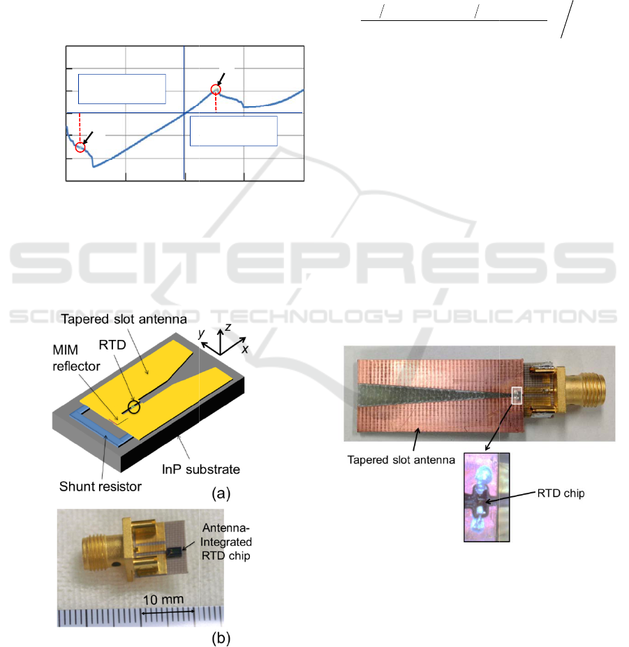
asymmetric with a polarity of DC
v
as shown in Fig. 2. A wide n
e
(NDR) region (Point A) is suitabl
e
operation, while the peak point
w
polarity (Point B) is appropriate
operation.
Usually, the RTD is integrat
e
antenna such as dipole and tape
r
The antenna-integrated RTD chip
i
coplanar waveguide substrate
w
connector via bonding wire as sho
w
Figure 2: DC I-V characteristics of the
points for transmitter (A) and receiver
(
Figure 3: (a) Schematic of antenna-i
n
Photograph of a connectorised RTD m
o
電圧(V)
電流(mA)
Operation point
for transmitter
O
10
0
-10
-1.0 -0.5 0
DC volta
g
DC current (mA)
A
v
oltage or current
e
gative resistance
e
to the oscillator
w
ith the opposite
for the detector
e
d with a planar
r
ed slot antennas.
i
s mounted on the
w
ith the co-axial
w
n in Fig. 3.
RTD and operation
(
B).
n
tegrated RTD. (b)
o
dule.
3 APPLICATIONS
T
RECEIVERS
3.1 Responsivity Eval
u
Receiver responsivity can be
e
characteristics based on the
theory (Cowley and Sorenso
n
power is expressed in the case
() ()
64)(4
)1(
4)2(2
⎩
⎨
⎧
+
=
f
f
AVfA
P
Bias
where f(V) (= I) is the I-V fu
n
are derivatives of f(V) with re
s
amplitude of the input radio
fr
applied to the RTD.
We have conducted the e
x
above theory
b
y using the r
e
the RTD chip is bonded to a
t
a glass epoxy substrate (FR-4
)
order to evaluate an intrins
i
RTD avoiding the influence
o
parasitic elements, 35-GHz si
g
the module with the RTD ch
i
frequency above 300 GHz.
amplitude-modulated at 100
k
signals by the receiver was
m
analyzer tuned at 100 kHz.
Figure 4: Photograph of the RT
D
GHz experiment.
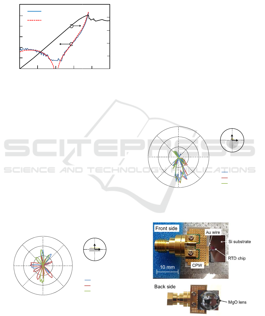
Figure 5 shows a depen
d
power measured as a function
The DC I-V characteristics
a
figure. A solid line (measur
e
(calculated) agree quite well.
O
peration point
for receiver
0.5 1.0
g
e (V)
B
T
O
u
ation
e
stimated from DC I-V
square-low detection
n
, 1966). The detected
of 50-ohm load as
50
)(
2
)4(
⎭
⎬
⎫
V
f
Bias
(1),
n
ction, f
(1)
, f
(2)
, and f
(4)
s
pect to V, and A is an
fr
equency (RF) voltage
x
perimen
t
to verify the
e
ceiver module, where
t
apered slot antenna on
)
as shown in Fig. 4. In
i
c responsivity of the
o
f a conductor loss and
g
nals were received by
i
p which has a cut-off
35-GHz signals were
k
Hz, and demodulated
m
easured by a spectrum
D
receiver module for 35-
d
ence of the received
of the DC bias voltage.
a
re also plotted in the
e
d) and a broken one
Relative responsivity
Third International Conference on Telecommunications and Remote Sensing
42
b
ecomes maximum at the peak v
o
the NDR region as expected. In th
e
output voltage becomes unstable
a
increases.
Figure 5: Relative responsivity and
function of DC bias voltage.
3.2 Receiver Modules
We simulated antenna radiati
o
RTD chip of Fig. 3(a) (1.9 mm lo
and 0.6 mm thick) for frequencies
GHz, and 305 GHz, by finite
-
domain (FDTD) method as shown
relatively thick InP substrate wit
h
dielectric constant, ε
r
(12.1), the
r
become diverse and vary consi
d
frequency. The electromagnetic
propagate along the tapered slot
attracted into the InP substrate
(
1989), which results in Fabry-Pero
t
the substrate, and a maximum an
t
dBi.
Figure 6: Simulated antenna
p
atterns
RTD chip shown in Fig. 3 for various
fr
0 50 100 150
-50
-60
-70
-80
-90
-100
-110
Measured
Calculated
DC Voltage (mV)
Relative Power (dBm)
5 10 15
-135°
-45°
±180°
45°
90°
135°
(dBi)
0°
-90°
90°
o
ltage just before
e
NDR region, the
a
nd a noise level
DC current as a
o
n patterns of the
ng, 0.9 mm wide
of 295 GHz, 300
-
difference time-
in Fig. 6. Due to
h
a high relative
r
adiation patterns
d
erably with the
waves do not
antenna, but are
(
Yngveson et al.,
t
resonance inside
t
enna gain of 8.8
on H-plane of the
fr
equencies.
We examined an integrat
i
hemispherical lens (Nakajim
a
RTD chip in order to impro
v
Attaching a hyper-hemisphe
r
can lead to the efficient coupl
i
the free space from the subst
r
effect and low aberration (V
a
The reflection at the InP-M
g
since the relative dielectric c
o
9.7 for 300 GHz, which is c
l
substrate. MgO is almost tra
n
waves and visible light. Thus
w
the lens while aligning the po
s
The chip is glued to the center
the lens by ultraviolet cure ad
h
the simulated antenna
p
atte
r
integrated with the MgO le
n
almost the same for 290–30
0
antenna gain is 12.5 dBi.
Figure 8 shows photograp
h
module with the MgO lens.
Figure 7: Simulated antenna
p
a
t
RTD chip with MgO lens for vari
o
Figure 8: Photographs of the R
T
MgO lens.
200 250
2.5
2.0
1.5
1.0
0.5
0
DC Current (mA)
295 GHz
300 GHz
305 GHz
-90°
0°
±180°
z
x
5 10 15
-1
3
-4
5
±180°
45°
90°
135°
(dBi
)
0°
i
on of an MgO hyper-
a
et al., 2004) with the
v
e the antenna pattern.
r
ical lens to substrate
i
ng of THz radiation to
r
ate with a collimation
a
n Rudd et al., 2002).
g
O interface is small
o
nstant of MgO is ε
r
~
l
ose to that of the InP
n
sparent both for THz
w
e can easily integrate
s
ition of the RTD chip.
of the cross-section of
h
esive. Figure 7 shows
r
ns of the RTD chip
n
s. The directivity is
0
GHz. The maximum
h
s of the RTD receiver
t
terns on H-plane of the
o
us frequencies.
T
D receiver module with
3
5°
5
°
295 GHz
300 GHz
305 GHz
)
-90°
90° -90°
0°
±180°
z
x
Terahertz Wireless Communications Using Resonant Tunneling Diodes as Transmitters and Receivers
43
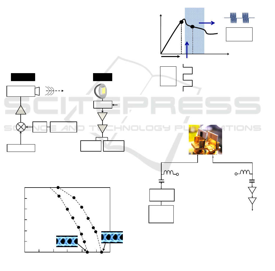
We conducted wireless transmission experiments
using a frequency-multiplier-based transmitter and
the RTD receiver. Figure 9 depicts a schematic
diagram of the experimental setup. The output signal
from the up-converter, which mixes the RF signal
from a synthesizer (32–36 GHz) and the digital
signal from a pulse-pattern generator, is multiplied
by nine times to generate THz signals at 288–324
GHz. THz signals are radiated into the free space by
a horn antenna (25 dBi), and are detected by the
RTD receiver module. Demodulated signals are
amplified and re-shaped by a preamplifier and a
limiting amplifier, respectively.
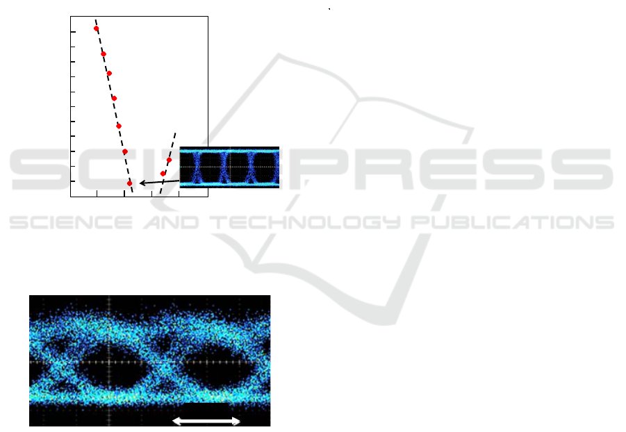
Figure 10 shows bit error rate (BER)
characteristics and eye diagrams. Error-free
(BER<10
-11
) transmission has been confirmed up to
the bit rate of about 11 Gbit/s. Currently, the
maximum bit rate is limited by the modulation
bandwidth of the transmitter based on the frequency
multiplier. Our design of the receiver module
ensures the bit rate of over 20 Gbit/s.
Figure 9: Block diagram of wireless transmission
experiment using a frequency-multiplier-based transmitter
and the RTD receiver.
Figure 10: Bit error rate characteristics and eye diagrams
at 300 GHz.
4 APPLICATIONS TO ALL RTD-
BASED TRANSCEIVERS
For the operation of the RTD as a transmitter, the
amplitude of the applied voltage is changed to
perform the on-off keying (OOK) modulation as
shown in Fig. 11. The amplitude of both the DC bias
and RF modulation voltages was carefully adjusted
so that the output power from the RTD became
maximum (Mukai et al., 2011).
Figure 11: Operation of the RTD as a transmitter with
OOK modulation scheme.
Figure 12: Experimental setup of proximity wireless
transmission experiment using two sets of RTD modules.
By using two sets of RTD modules without MgO
lens (Fig. 3(b)), we conducted a close-proximity
wireless transmission experiment, placing the two
modules at a distance from a few millimeters to
several tens of millimeters as shown in Fig. 12. For
Synthesizer
Pulse-pattern
generator
Amplifier
Preamplifier
Atten.
Oscillo-
scope
Error
detector
Limiting
amplifier
IF
LO
RTD
Bias-tee
Up-converter
Frequency
Multiplier (x9)
DC bias
Transmitter Receiver
1E-10
1E-8
1E-6
8 9 10 11
Bit error rate
10.75 Gbit/s
10 Gbit/s
LO power (dBm)
DC Current
DC Voltage
01001
0
1
1
0
0
Input
data
signal
Modulated
THz signal
Bias
Oscillation
region
Preamp.
Limit amp.
DC bias
DC bias
Variable
attenuator
To oscilloscope
and error detector
RTD transmitter
RTD receiver
Blocking capacitor
Pulse
pattern
generator
Third International Conference on Telecommunications and Remote Sensing
44
the transmitter, the data signal (RF voltage) from the
pulse-pattern generator was applied to the module
with an appropriate DC bias voltage through a bias-
T. For the receiver, just a DC bias voltage was
applied to the RTD to maximize the sensitivity. The
demodulated baseband data signal was amplified
with the preamplifier followed by the limiting
amplifier.
The oscillation frequency depends on the parallel
inductance and capacitance of RTD chip, and the
output power is proportional to the widths of the
current and voltage of the NDR region (Asada et al.,
2008). The oscillation frequency and the output
power of the RTD used for the experiments were
approximately 300 GHz and several μW,
respectively.
Figure 13: BER characteristics plotted against the DC bias
voltage and eye diagram at 1.5 Gbit/s.
Figure 14: Demodulated eye diagram at 2.5 Gbit/s.
Figure 13 shows a dependence of the BER on the
applied DC bias voltage when the amplitude of the
data signal was 160 mVp-p. At 0.85 V, an error-free
transmission at 1.5 Gbit/s was achieved as shown in
the eye diagram of Fig. 13. There were optimum DC
bias voltages depending on the RF voltage
amplitude. By carefully adjusting the DC bias
voltage, the achieved maximum data rate was 2.5
Gbit/s (Fig. 14), which is mainly limited by the
frequency-dependent radiation pattern as discussed
in Sec. 3.2, and the bandwidth of the packaging
(Shiode et al., 2011, 2012). Use of RTD transceiver
modules with MgO lens will increase the bit rate
over 10 Gbit/s.
5 CONCLUSIONS
We have described a small and cost-effective
transceiver module employing resonant-tunnelling
diodes (RTDs) towards wide-spread consumer THz
wireless applications such as a close-proximity
instantaneous data transfer and a wireless
interconnection.
The RTD-based receiver module with MgO
hyper-hemispherical lens has exhibited over 10-
Gbit/s performance at 300 GHz. Using the RTD-
based transmitter and receiver, a close-proximity
wireless transmission at 2.5 Gbit/s has been
demonstrated with an error-free condition. Future
works should be placed on the increase of data rate
and transmission distance by improving the
packaging and the antenna structure, respectively.
ACKNOWLEDGEMENT
This work was supported in part by the Strategic
Information and Communications R&D Promotion
Programme (SCOPE), from the Ministry of Internal
Affairs and Communications, Japan.
REFERENCES
Asada, M., Suzuki S., Kishimoto, N., 2008. Resonant
tunneling diodes for sub-terahertz and terahertz
oscillators. Jpn. J. Appl. Phys., Vol. 47, No. 6, pp.
4375–4384, 2008.
Cowley A. M., Sorenson, H. O., 1966. Quantitative
comparison of solid-state microwave detectors. IEEE
Trans. Microwave Theory and Tech., vol. 14, pp.
588–602.
Kleine-Ostmann, T., Nagatsuma, T., 2011. A review on
terahertz communications research. J. Infrared Milli.
Terhz. Waves, vol. 32, no. 2, pp. 143–171.
Mukai T., M. Kawamura, M., Takada, T., Nagatsuma, T.,
2011. 1.5-Gbps wireless transmission using resonant
tunneling diodes at 300 GHz. Tech. Dig. Optical
Terahertz Science and Technology (OTST2011),
MF42, Santa Barbara.
Bit error rate
0.7 0.8 0.9
DC bias voltage (V)
1.5 Gbit/s
1E-2
1E-4
1E-6
1E-8
1E-10
1E-12
1
250 ps
Terahertz Wireless Communications Using Resonant Tunneling Diodes as Transmitters and Receivers
45

Nagatsuma, T., Ito, H., Ishibashi, T., 2009. High-power
RF photodiodes and their applications. Laser Photon.
Rev., vol. 3, no. 1-2, pp. 123–137.
Nagatsuma, T. et al., 2013. Terahertz communications
based on photonics technologies, Optics Express, vol.
21, no. 20, pp. 23736–23747.
Nakajima, M., Uchida, K., Tani, M., Hangyo, M., 2004.
Strong enhancement of terahertz radiation from
semiconductor surfaces using MgO hemispherical
lens coupler. Appl. Phys. Lett., vol. 85, no. 2, pp.
191–193.
Shiode, T., Mukai, T., Kawamura, M., Nagatsuma, T.,
2011. Giga-bit wireless communication at 300 GHz
using resonant tunneling diode detector. Proc. Asia-
Pacific Microwave Conference (APMC2011),
Melbourne.
Shiode, T., Kawamura, M., Mukai, T., Nagatsuma, T.,
2012. Resonant-tunneling diode transceiver for 300
GHz-band wireless link. Tech. Dig. Asia-Pacific
Microwave Photonics Conf. (APMP2012), WC-1,
Kyoto.
Song, H.-J., Nagatsuma, T., 2011. Present and future of
terahertz communications. IEEE Trans. Terahertz
Science and Technology, vol.1, no. 1, 256–264.
Suzuki, S., Asada, M., Teranishi, A., Sugiyama H.,
Yokoyama, H., 2010. Fundamental oscillation of
resonant tunneling diodes above 1 THz at room
temperature. Applied Physics Letters, vol. 97, no. 24,
pp. 242102–242102-3.
Van Rudd J., Mittleman, D. M., 2002. Influence of
substrate-lens design in terahertz time-domain
spectroscopy. J. Opt. Soc. Am. B, vol. 19, no. 2, pp.
319–328.
Yngveson, K. S., Korzeniowski, T. L., Kim, Y.-S.,
Kollberg, E. L., Johansson, J. F., 1989. The tapered
slot antenna- A new integrated element for
millimeter-wave applications. IEEE Trans.
Microwave Theory and Tech., vol. 37, no. 2, pp. 365–
374.
Third International Conference on Telecommunications and Remote Sensing
46
