
High Voltage Integrated Chip Power Recovering Topology for
Implantable Wireless Biomedical Devices
Vijith Vijayakumaran Nair, Jinhwan Youn and Jun Rim Choi
Department of Electronics Engineering, Kyungpook National University, Daegu, South Korea
Keywords:
Biomedical Implant, Power Recovery, High Voltage Integrated Chip, Cuff-Nerve Electrode Interface, Power
Efficiency, Rectifier, Linear Voltage Regulator, Charging Control Circuit.
Abstract:
In near field wireless power links for biomedical implants, inductive voltage at receiver end (Rx) largely
exceeds the compliance of low voltage integrated power recovery circuits. To limit the magnitude of induced
signal, most of the low voltage (LV) integrated power recovery schemes employ methods like voltage clipping
and shunt regulation. These methods are proved to be power inefficient. Therefore, to overcome the voltage
limitation and to improve the power efficiency, we propose an on-chip high-voltage (HV) power recovery
scheme based on step-down approach, which allows supply voltage as high as 30V. The proposed design
comprises of enhanced semi-active HV bridge rectifier, reference voltage generator and HV series voltage
regulator. In addition, a battery management circuit that ensures safe and reliable charging of the implant
battery is proposed and implemented. The proposed design is fabricated with 0.35µm HV BCD technology
based on LOCOS 0.35µm CMOS process. Rectifier and regulator power efficacy are analyzed and compared
through simulation and measurement results.
1 INTRODUCTION
Biomedical implants with power consuming devices
require near-field wireless power transmission links
to increase the battery operation lifetime. In applica-
tions such as neural stimulator, power is transmitted
through inductive links (Lee and Ghovanloo, 2011;
Li et al., 2013; Mouna¨ım and Sawan, 2011).The near-
field inductive link provides sufficient power to meet
high simulation current requirements and to address
the large electrode nerve interface impedance in the
biomicrosystem. However, during periods of low cur-
rent simulation, the recovered voltage at the Rx may
largely exceeds the compliance of the low-voltage in-
tegrated circuits (IC’s). Hence, to protect these kind
of systems, traditionally Zener diodes or on-chip volt-
age limiters as in (Balachandran and Barnett, 2006;
Lee and Ghovanloo, 2011; Su et al., 2012) or shunt
regulators as in (Wang et al., 2005) are used. These
approaches limit the supply voltage to below 5.5 V
and the power efficiency is low as most of the excess
power is converted to current, which is dissipated as
heat.
Moreover, for stimuli generator in the implantable
device, the cuff electrode-nerve interface impedance
increases over the course of time (Thil et al., 2004;
Li et al., 2005; Mouna¨ım and Sawan, 2011; Mounaim
and Sawan, 2012; Li et al., 2013). As a result, thecon-
ventional low supply voltages are insufficient to pro-
vide enough simulation current. In order to provide
the required simulation current, typically in the range
of 1−2mA, the supply stimulus voltage should be cor-
respondingly raised to higher level. Therefore, the
designed prior low voltage power recovery schemes
in the existing literature (Balachandran and Barnett,
2006; Lee and Ghovanloo, 2011; Su et al., 2012;
Wang et al., 2005) become unsuitable for the imple-
mentation. Considering the real time system for neu-
ral stimulator (Current>800µA from 3.7V, 2mA stim-
ulation pulses from 12V and R
S
=12.67KΩ) and em-
ploying the theoretical study published in (Nicolson
and Phang, 2004), the step down method proves to
be more efficient if the converter efficiency is greater
than 45%, and output impedance is less than 10KΩ.
The possible solution can be an approach based on
IC that would not limit the received voltage at the
Rx end. Power recovery circuit when realized in
HV technology could withstand high operating volt-
ages. Further, it will essentially serve the advantage
of storing the excess power in filter capacitor (pro-
ceeding rectification), leading to higher rectified volt-
age. Where as in voltage limiting structures, exces-
sive received power is heat dissipated. Hence, limiter
(Balachandran and Barnett, 2006) and shunt regulator
13
Vijayakumaran Nair V., Youn J. and Choi J..
High Voltage Integrated Chip Power Recovering Topology for Implantable Wireless Biomedical Devices.
DOI: 10.5220/0005194000130022
In Proceedings of the International Conference on Biomedical Electronics and Devices (BIODEVICES-2015), pages 13-22
ISBN: 978-989-758-071-0
Copyright
c
2015 SCITEPRESS (Science and Technology Publications, Lda.)
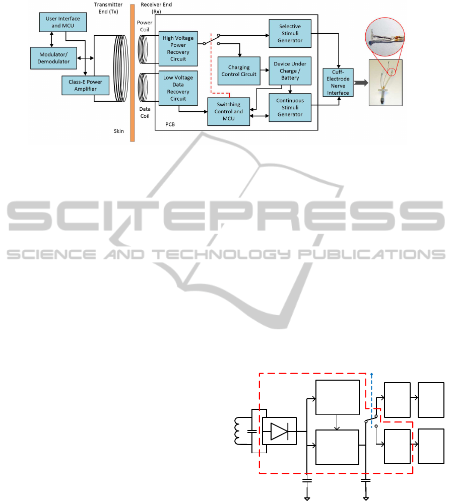
Figure 1: Block diagram of wireless power and data transfer chain for neurostimulator.
(Wang et al., 2005) have been successively replaced
by a step-down buck converter. But, the buck con-
verter requires a large value inductor which is not fea-
sible to incorporate on-chip. Moreover, maintaining
the regulation quality and efficiency is a difficult task
at high operating frequency (Tomita et al., 2012). An
alternative and more suitable solution is to replace the
shunt regulator and buck converter with a high input
series voltage regulator. The input voltage in series
regulator is limited only by the available power at the
Rx and the total power consumption that includes the
series regulator dissipation.
In (Mouna¨ım and Sawan, 2011; Mounaim and
Sawan, 2012), IC based on HV technology for power
recovery in implantable device showed improved
power efficiency based on simulation results. A HV
IC power recovery system for contactless memory
card (Tomita et al., 2012) reported 50% power effi-
ciency at higher input power level. But, the system
feature size and its low power efficiency made it un-
suitable for biomedical applications.
This paper proposes the design and fabrication of
on-chip power recovery analog front end in HV tech-
nology. The design is based on voltage step down
approach. The system is detailed in the following sec-
tions. Section 2 describes the proposed topology, Sec-
tion 3 details the circuit design methodology, section
4 presents the simulation and measurement results
and section 5 the conclusion. The IC is fabricated
in 5060BD35BA bipolar-CMOS-DMOS 0.35µm 60V
Mixed Technology in Dongbu Hi-tek process. The
prototype fabricated can be used for the purpose of
generating stimulus current and recharging battery in
biomedical implants.
2 PROPOSED TOPOLOGY
Figure 1 shows the conventional wireless power/data
transmission chain for neural stimulator. The ex-
ternal block which consists of user interface, mi-
cro controller unit (MCU) and the data modula-
tor/demodulator enable the user to monitor and con-
trol the power/data transmission and the class-E type
amplifier generates power signal based on the stim-
ulation current requirements. The power recovery
block receives the power at Rx coil and supplies the
power to charge implant battery and generates essen-
tial high current stimuli. Data recovery block receives
the command from the user and sends the feedback.
Switching control and MCU within implant, control
and monitor various modes of operation by interpret-
ing the user commands. Charging control circuit en-
ables safe and reliable recharging of implant battery
that powers the MCU and also generates continuous
low current stimuli for nerve repair.
Adjustable
Series Voltage
Regulator 8 V,
4 V (LDO)
High Voltage
Bridge
Rectifier
Filter
Capacitor
Load Coil/
Antennae.
RF power
Receiver
L
C
Wide input
range multiple
output Voltage
and Current
Reference
Charging
Control
Circuit
Load
Capacitor
V
DC
up to
30 V
V
DD
Stimulus
Current
generator
Switch Control
Proposed work
Device
Under
Charge
Cuff-
Nerve
Electrode
Interface
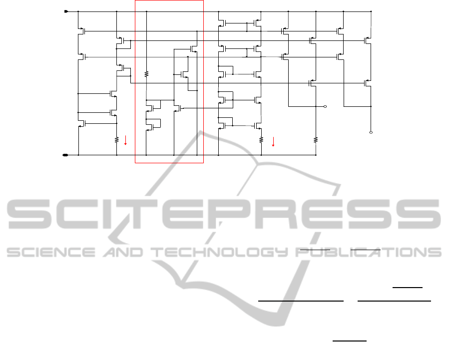
Figure 2: Schematic block of power recovery topology in
neurostimulator.
Figure 2 shows the proposed and implemented power
recovery module for the neural stimulator. The de-
sign which is based on step down approach is detailed
in the following sections. The rectifier converts HV
AC signal to DC, which is then supplied to the low
drop out (LDO) voltage regulator that steps down the
high voltage to the desired voltage level. The refer-
ence circuit generates the necessary reference voltage
BIODEVICES2015-InternationalConferenceonBiomedicalElectronicsandDevices
14

and current for the LDO and charging control circuit.
The LDO output is coupled to the high current stimu-
lus generator aiding nerve repair and charging control
circuit, by means of a switch.
2.1 Design Specification
As power efficiency in biomedical implants is of high
significance, the design constraints are more criti-
cal. The total power efficiency (η
total
) of the wireless
power system is given by
η
total
= η
supply
+ η
coils
+ η
recti
+ η
LDO
+ η
ctrl/sti
(1)
where η
supply
is efficiency of the radio frequency
(RF) power amplifier/generator, η
coils
is the power
transmission efficiency of the wireless link, η
recti
is
the power conversion efficiency (PCE) of the recti-
fier, η
LDO
is the LDO regulator efficiency, η
ctrl
is the
power efficiency of the charging control circuit and
η
sti
is the power efficiency of stimulus generator. The
charging of the battery and nerve stimulation occurs
at differnt time instances.
The biomicrosystem generates stimulus in the
form of pulse currents. For the neural stimulation,
the pulse currents magnitude is ranging from 1-2mA
(Mouna¨ım and Sawan, 2011; Li et al., 2013). In gen-
eral, low voltage supply favors the neural stimula-
tion when the cuff-nerve impedance is low. But, few
months after the implantation, magnitude of the cuff-
nerve interface’s impedance rises to 2−8KΩ (Thil
et al., 2004; Li et al., 2005; Mouna¨ım and Sawan,
2011; Mounaim and Sawan, 2012; Li et al., 2013).
Under these circumstances to generate the necessary
simulation currents, the supply voltage must be in-
creased. Typically, it is from the range 3.3−5V to
10−20V. Rest of the system functions with typical
low voltage supply from the battery. The continu-
ous stimuli generator is powered by battery and es-
sentially uses lesser than 30µA current pulse at 100Hz
(Li et al., 2013). In practice, batteries rating of 3.7V
and 20mAh are used in biomedical implants due to
their smaller size and low power requirements. Ac-
cording to our design specifications, a charging cur-
rent of 10mA is required to enable quick charging of
the battery.
3 CIRCUIT DESIGN METHODS
3.1 Semi-active HV Bridge Rectifier
Conventionally, implementation of a full wave bridge
rectifier involves diode connected MOS transistors
V
AC2
V
AC1
RL
HVM1
V
DC
CL
GND
GND
HVM2
HVM3
HVM4
HVM5
HVM6
Cb1
Cb2
Rb1
Rb2
Figure 3: Circuit schematic of the proposed high voltage
rectifier.
in CMOS technology. Further, rectifiers based on
threshold cancellation techniques (Nakamoto et al.,
2007) and cross-coupled structure (Mandal and
Sarpeshkar, 2007) are also proposed in CMOS tech-
nology. These schemes provide efficient rectifica-
tion, but the reported PCE is < 70%. Followed by
the cross-coupled topology, a series of works based
on comparator technique are reported (Guo and Lee,
2009; Lee and Ghovanloo, 2011; Cha et al., 2012).
But, the PCE response plot rapidly decrease with fre-
quency above 10MHz. The earlier works are unsuit-
able for the intended application due to the power
constraints, low operating frequencies, complicated
circuit calibration and comparably low PCE. In ad-
dition, the main constraint that limits the implemen-
tation of earlier work in our HV design approach is
the gate-to-source voltage (V
GS
) limitation (maximum
V
GS
Dongbu BCD process=13.2V). Design of active
rectifier in this technology requires level shifters that
affects the total efficiency. Apart from this, level
shifters are conventionally designed for specific input
voltages. In (Mouna¨ım and Sawan, 2011), the work
shows the design of HV rectifier and the simulation
result reports 93% PCE, butV
GS
limitation holds from
implementation in our technology.
In this section, we explain the proposed semi-
active HV bridge rectifier based on partial and adap-
tive threshold cancellation techniques. The schematic
diagram of the proposed rectifier is depicted in Figure
3. The gate of the HV LDNMOS transistors, HVM3
and HVM4 are biased with cross-coupled resistors
(Rb1, Rb2), diode connected transistors (HVM5,
HVM6), and bias capacitors (Cb1, Cb2). The dy-
namic bias voltage tracks the threshold voltage (V
th
)
of HVM5 and HVM6 through various temperature
and process conditions. The average value of the bias
voltage is lower than the V
th
of transistors HVM3 and
HVM4. The desired bias voltage is obtained by ap-
propriately sizing the bias transistors, resistors, and
capacitors. Increasing the bias voltage in the conduc-
HighVoltageIntegratedChipPowerRecoveringTopologyforImplantableWirelessBiomedicalDevices
15
LVM1
LVM6
HVM5
HVM2
HVM3
LVM3
LVM10
LVM12
HVM10
LVM7
HVM7
HVM6
LVM9
GND
V
DDH
I
REF
V
REF
I
B
I
A
HVM1
LVM4
LV
M2
LVM5
HVM4
LVM11
HVM9
LVM8
LVM13
LVM14
LVM15
LVM16
HVM14
HVM12
HVM13
HVM11
HVM8
R1 R2 R3
R4
Start -up Circuit
Figure 4: Circuit schematic of voltage and current reference generator.
tion phase decreases the on-resistance of the power
transistors, but increases the leakage current through
the off transistor and thus decreasing the PCE. There-
fore, the complete V
th
cancellation is not a viable op-
tion for the design. In our design, the average bias
voltage about 65% ofV
th
of power transistors is main-
tained. The bias voltage adaptively increases to 90%
of the V
th
in the conduction phase and decreases to
40% in the non-conduction phase providing higher
power efficiency.
The bidirectional HV PMOS is connected as diode
connected transistor, due to the V
GS
limitation in our
process library. Unlike prior designs (Mouna¨ım and
Sawan, 2011; Mounaim and Sawan, 2012), the pro-
posed design does not limit the supply voltage and
moreover the average voltage drop is less than two
diode voltage drops. In our technology as the source
and bulk of the HV transistors are internally con-
nected, bulk biasing cannot be implemented that adds
to the limitation for attaining higher PCE.
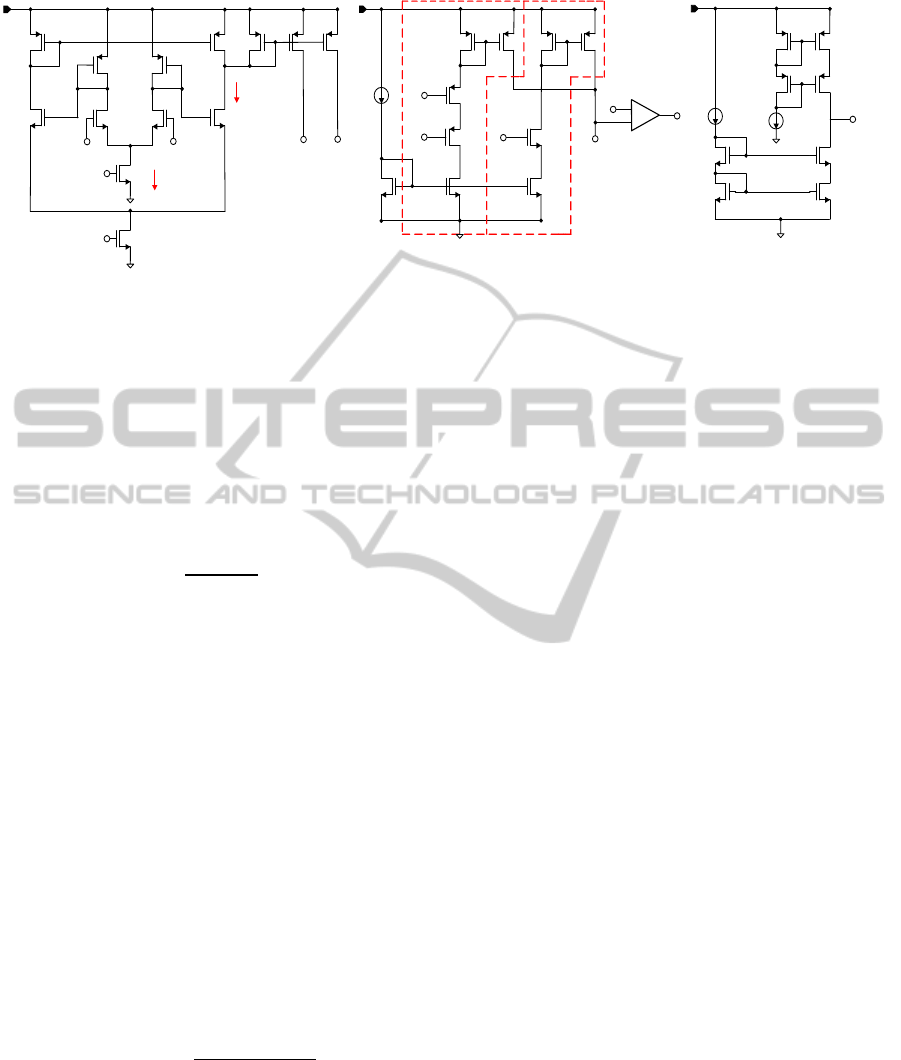
3.2 Voltage and Current Reference
The HV reference and current generators are fab-
ricated based on subthreshold MOSFET technique
(Huang et al., 2006). The LV-HV transistor cascading
scheme (Ballan et al., 1994) is employed to realize the
supply and temperature independent voltage and cur-
rent references. The transistors LVM11 and LVM12
operating in subthreshold regime generate a propor-
tional to absolute temperature (PTAT) current I
A
inde-
pendent of supply voltage variations. Further, LVM4
is also operated in subthreshold regime, which gener-
ates a complementaryto absolute temperature (CTAT)
current I
B
independent of variations in input voltage.
Figure 4 shows the schematic representation of the
designed high-voltagereference and current generator
with the essential startup circuitry. Currents I
A
and I
B
are summed to generate the supply voltage indepen-
dent and zero temperature coefficient current I
REF
.
Therefore, the reference voltage is expressed as
V
REF
=
K
LVM13
K
LVM8
I
A
+
K
LVM14
K
LVM2
I
B
R3 (2)
with
I
A
=
V
GSLVM11
−V
GSLVM12
R2
=
ζU
T
ln
K
LVM11
K
LVM12
R2
(3)
I
B
=
V
GSLVM4
R1
(4)
where, K
LVM
is aspect ratio of the transistors, R
is the resistor values, V
GS
is the gate to source volt-
age, ζ > 1 is a non-ideal factor, and U
T
= KT/q is the
thermal voltage.
3.3 High Voltage Linear Regulator
The designed HV LDO provides4V output, which de-
livers a maximum current of 100mA with input volt-
age of 30V. It is composed of a HV pass transistor
for low dropout, an error amplifier, resistor feedback
network and an output capacitor. The fabricated HV
series regulator utilizes cascode compensation, pop-
ularly known as Ahuja compensation. This employs
Miller compensation with common gate transistor as
current buffer that effectively replaces RHP zero with
LHP zero providing improved stability (Garimella
et al., 2011). The LV-HV transistor cascading scheme
(Ballan et al., 1994), is employed for the design of
the error amplifier. For the error amplifier design as
in (Garimella et al., 2011), the low voltage differ-
ential pair transistors and common gate transistor in
buffer stage are replaced by HV n-type LDMOS tran-
sistors with floating source to accommodate for high
BIODEVICES2015-InternationalConferenceonBiomedicalElectronicsandDevices
16
GND
V
DDH
V
OUT
I
REF
HVM1
HVM2 HVM3
HVM4
HVM6
HVM5
LVM1 LVM2
LVM3
LVM4 LVM5
LVM6
LVM9
I
OUT
R
oc
C1
C2
C
OUT
R
ESR
C
comp
V
BIAS
V
REF
V
REF
I
A
I
A
V
A
HVM7 HVM8
V
BIAS1
Pass
Transistor
R
FB2
R
FB1
Figure 5: Schematic diagram of the implemented HV LDO.
input voltage conditions. Cascade PMOS transistors
(LVM 1−2, HVM 7−8 shown in Fig.5) in differen-
tial pair stage are employed to increase the error am-
plifier gain. An n-type LDMOS transistor is used as
pass transistor to reduce the area of the pass device
three times compared to the p-type device in our tech-
nology. The total current consumption of the design
is limited to less than 170 µA. Figure 5 represents the
circuit schematic of the LDO with the over current
protection circuit.
The on-chip capacitor used for the compensation
could withstand voltage up to 35 V (break-down volt-
age), ensured safe operation within the design speci-
fications. Transistor HM4 is a cascode transistor, that
helps in reducing the drain to source voltage (V
DS
)
mismatch between LM3 and LM5, thus effectively
decreasing the DC bias current mismatch. Current I
A
is a scaled version of the bias current of the error am-
plifier, so as to reduce the total quiescent current. To
suppress the high frequency noise adequately, capac-
itors C
1
and C
2
are connected in parallel to the feed-
back resistors R
FB2
and R
FB1
respectively. The values
of the feedback resistors are determined based on the
reference voltage, output voltage and the resistor bias
current (Rincon-Mora and Gabriel, 2009). Further, an
additional circuit to limit the output current is placed
before the pass transistor that provides over current
protection.
The HV Dongbu Hi-tek technology offers limited
functionality in transistor sizing. Consequently, op-
timization of the error amplifier in the LDO is dif-
ficult as the transistor parameters are fixed. Particu-
larly when the input variations are large, the stability
and performance must be ensured.
3.4 Charging Control Circuit
In biomedical implants, battery management circuits
are inevitable to prolong the battery life time. Various
circuit architectures are proposed and implemented in
prior works based on digital and analog control for the
purpose of charging the batteries (Chen and Rincon-
Mora, 2006; Li and Bashirullah, 2007). These de-
signs may utilize expensive precision sense resistors
or analog-to-digital converters that occupy large area
for end of charge (EOC) detection.
EOC
Detector
Trickle
Charge
Flag
Current
Gain
Battery
OTA
Comparator
+
-
V
Battery
V
Ref2
V
Ref1
Figure 6: Block schematic of battery charger.
In (Do Valle et al., 2011), a compact lithium-
ion (Li-ion) battery charger based on analog con-
trol is reported. This design overcame the demer-
its of prior designs and addressed to all the four
(Trickle charging, constant current (CC), constant
voltage (CV) and EOC) charging regimes. But, the
designed subthreshold operational transconductance
amplifier (OTA), that determines the linear voltage
range (approximately 100mV) is directly dependent
on the temperature. Temperature fluctuations vary the
linear voltage range of tanh function, that results in
either overcharging or undercharging of the implant
battery. This irregularities may decrease battery life
time. To overcome the temperature artifacts on linear
voltage range, we propose a charger based on adap-
tive bias OTA, where transistors are operating in sat-
uration region. The simplified block diagram of the
charging is shown in Figure 6.
HighVoltageIntegratedChipPowerRecoveringTopologyforImplantableWirelessBiomedicalDevices
17
LVM1
LVM7
LVM8
V
DD
LVM2
LVM3 LVM4
LVM5 LVM6
LVM9
LVM10
LVM11
LVM12
LVM13
V
B1
V
B2
V
Ref1
V
Battery
EOC input
Current
gain
input
V
DD
LVM14
LVM19
LVM15
LVM16
LVM17
LVM20
LVM21
LVM23
V
Battery
V
Ref2
V
trickle
V
trickle
V
trickle
+
-
EOC output
Current
gain
input
LVM18
LVM22
Current gain-
stage 1
Current gain-
stage 2
LVM25
LVM27
LVM28 LVM29
V
DD
EOC
input
EOC
output
LVM24
LVM30
LVM31
LVM26
I
REF1
Comparator
(a)
(b) (C)
I
B1
I
out
Figure 7: Schematic diagram of (a) OTA, (b) Current gain stage and trickle charge detector, (c) EOC detector.
The OTA in Figure 7(a) (Do Valle et al., 2011),
is designed to operate in saturation region where the
output current is a function of tanh. The output cur-
rent is generated based on comparison of the battery
voltage to reference. By operating the OTA in satu-
ration regime, the linear voltage range is controlled
adaptively by the bias voltage V
B1
. The linear voltage
range of the OTA is given by
V
L
=
V
B1
−V
th
k
s
√
2
(5)
where V
B1
is the bias voltage and k
s
is the sub-
threshold exponential slope parameter . The bias volt-
age was fixed to be 810mV (V
th
=700mV) ensuring
the saturation region operation of the OTA and the
derived linear range was 160mV. Though V
th
in the
equation (5) has negative temperature coefficient, the
bias voltage derived from the CTAT current (equation
(4)) source in the reference generater compensates for
the decrease in threshold voltage, thus maintaining
the constant bias current I
A1
and linear range. The de-
sign maintains constant linear voltage range that pro-
tects the battery from overcharging.
The linear range signifies that for battery voltages
less than 3.54V, the OTA output is saturated allow-
ing maximum output current and for battery voltages
greater than 3.54V the OTA operates in the linear re-
gion implying decrease in output current. The output
current of the OTA is given by
I
out
= I
B1
tanh(
k
s
(V
in+
−V
in−
)
2U
T
) (6)
where I
out
is the output current of OTA, I
B1
is the bias
current of OTA, k
s
is the subthreshold exponential
slope parameter, V
in+
,V
in−
are the input voltages and
U
T
is the thermal voltage. The voltage reference
circuit described in earlier section generates zero
temperature coefficient supply independent voltage
(3.7V) in relative to the battery voltage used in the
biomedical implant.
The current gain circuit uses two separate mul-
tiplier transistors. The first multiplier is turned on
during the CC regime and has higher current gain and
the second multiplier operates at the time of trickle
charging providing lower gain. In CC regime the
charging current is designed to be 10mA and 1mA
during trickle charging. Since the OTA is operated in
the saturation regime (bias current 20µA) the current
gain stage is compact and shows good stability in
high power designs. In CC regime, LVM17 and
LVM18 (Figure 7(b)) are conducting, which enables
first current gain stage and 10mA current charges the
battery.
The Trickle charge detector circuit comprises of a
simple comparator that compares the battery voltage
to a reference voltage. The comparator output is
high when the reference voltage (V
Ref 2
= 2.5 V) is
higher than the battery voltage. This output turns
on transistor LVM22 and turns off LVM18 (Figure
7(b)), thus enabling current through second gain
stage implying trickle charging.
The EOC detector shown in Figure 7(c) is de-
veloped as in (Rincon-Mora and Gabriel, 2009). It
compares the EOC input to a reference current. The
schematic of the current comparator is shown in the
Figure 7(c). The EOC output signal is at ground po-
tential when the EOC input is higher than the refer-
ence current, but changes to supply potential when
condition is not true and thus controls the charging
current.
BIODEVICES2015-InternationalConferenceonBiomedicalElectronicsandDevices
18
4 SIMULATION AND MEASURED
RESULTS
The proposed topology is implemented with 0.35µm
BCD process and simulations are performed in Ca-
dence Spectre environment. The AC input voltage
is set below 20V peak maximum for load currents
less than 2mA. But, when the system is directed to
charge the battery, the input voltage is varied between
4.5−7V peak with a load current of 9−11 mA and fil-
ter capacitor being 0.5µF. The bias voltage varies in
the range of 0.49−1.06 V in non-conduction and con-
duction phase ensures that the HVNMOS transistors
are operated in linear region (Dongbu 60V LDNMOS
V
th
= 1.2V). Figure 8 shows the experimental result of
the gate bias voltage of HVNMOS transistor for an
input voltage of 15 V peak.
Figure 8: Measurement result of dynamic bias voltage.
Rectifiers are often characterized with their PCE
and VCE. VCE is calculated based on the equation
V
OUT
/V
IN
. The PCE in all measurement and simu-
lation results in this paper is calculated based on the
equation (7).
η
PCE
=
V
OUT
∗I
OUT
P
in
=
V
2
OUT
∗T
R
L
R
T
0
V
in
(t) ∗I
in
(t)dt
. (7)
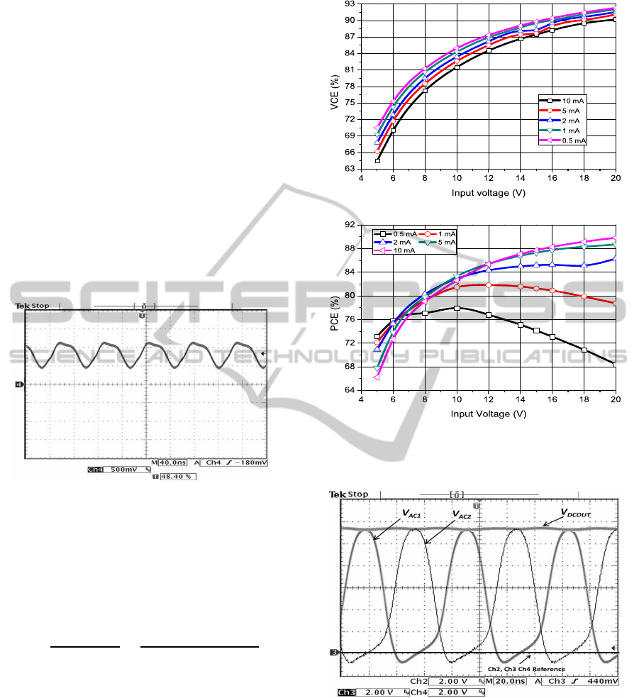
Figure 9(a) and 9(b) show the post-layout sim-
ulation results of VCE and PCE of the rectifier re-
spectively for various load currents with varying input
voltage. IC is tested using various values of discrete
resistors ranging from 0.5−8KΩ. Discrete resistors
were used to replicate the increasing cuff-nerve elec-
trode interface impedance. Oscilloscope capture of
the rectifier input and output node voltages at 13.56
MHz input frequencyand output load current of 1 mA
is shown in Figure 10.
The experimental results of VCE and PCE for
varying input voltage are depicted in Figures 11(a)
and 11(b) respectively. The voltage conversion ratio
(a)
(b)
Figure 9: Simulated (a) VCE and (b) PCE with varying in-
put voltage and load current.
Figure 10: Measurement result of voltage at nodes V
AC1
and V
AC2
and the DC output.
at low load currents resembles closely to the simula-
tion results. At high load currents and high supply
voltage, measured VCE and PCE deviate from sim-
ulation results. This is due to substrate leakage cur-
rent and results in latch-up which destroys the chip.
The existence of parasitic bipolar transistors that is
not modelled during the simulation proces, conducts
current when the reverse voltage exceeds certain limit
HighVoltageIntegratedChipPowerRecoveringTopologyforImplantableWirelessBiomedicalDevices
19
Table 1: Performance comparison with prior rectifiers.
Publication Guo Lee Mounaim Cha Proposed work
Technology
0.35µm 0.5µm DALSA 0.18µm 0.35µm
CMOS CMOS C08G-C08E CMOS BCD
V
in,peak
(V) 2.4 3.8 16.8 1.5 20.0
V
REC
(V) 2.28 3.12 15.5 1.33 17.32
Frequency (MHz) 0.2-1.5 13.56 13.56 13.56 13.56
R
Load
(KΩ) 0.1 0.5 5.0 1.0 0.5 to 8
Area(mm*mm) NA 0.18
4 and 9
0.009
2.5 x 5
(Total Chip) (Total Chip)
Load current I
L
(mA) 20 NA 10 NA 0.5 to 10
PCE (%) maximum 82-87 80.20
93.10
81.90 80.2
(Simulated)
(a)
(b)
Figure 11: Measured (a) VCE and (b) PCE with varying
input voltage and load current.
(Zou and T, 2012). The limit is set to -600mV in pro-
posed technology. Though, modelling of the parasitic
bipolar transistors have been explored in prior works
(for example: (Zou and T, 2012)), an accurate mod-
elling is still not developed due to the process varia-
tions in different technologies. This is a major limi-
tation for the implementation of bulk HV process and
is beyond the scope of this paper. The results shown
Figures 11(a) and 11(b) are based on operating points
where latch-up does not occur.
From the Figure 10, it can be observed that the
substrate leakage current is negligible since the rec-
tifier input never crosses the output DC voltage.
At high input voltages and load currents(I
load
>2mA
and V
in
peak>16V), the rectifier becomes abnormally
loaded and the input AC voltages become higher than
the output DC. However, in our application for stim-
ulus generator, the current required is ≤2mA with
input voltages ranging from 10−20V peak, the de-
sign proves to be more effective indicating higher
PCE compared to prior artworks. Meanwhile, for
recharging the implantable battery at low input volt-
ages (4.5−7 V) and high load currents (9−11 mA),
the maximum efficiency can be achieved as 63.2%. A
comparison of proposed work to prior works is shown
in Table 1.
The voltage and current references generate the
essential bias current and reference voltage for the
LDO. The reference voltages of 3V, 3.7V, 2.5V are
generated for LDO and charger circuit. The regulator
is designed to generate adjustable output voltage of
4V and 8V for an output load range 0.3−100mA.
Figure 12: Oscilloscope capture of HV regulators at startup.
Load capacitor of 1 µF is used for the measure-
BIODEVICES2015-InternationalConferenceonBiomedicalElectronicsandDevices
20
ment analysis of LDO. Though, on-chip resistor op-
tion is available for the technology, we used discrete
resistor divider network in our prototype to generate
the different output voltage. The LDO is tested for
4 V output for our specific application. Oscilloscope
capture of transient response of the LDO at start-up
is shown in the Figure 12. The output voltage is in-
dicated by channel 3 and input voltage by channel 4.
The regulator is stable for large input voltage varia-
tions. The summary of the experimental results are
shown in Table 2.
Table 2: Performance summary of the HV-Regulator.
Parameter Value Conditions
V
OUT
4 ± .07 V
V
IN
=6−30V;
I
OUT
=0.3−100mA
V
Dropout
164mV I
OUT
=1mA, V
OUT
=4V;
Mean 242mV I
OUT
=50mA,V
OUT
=4.03V
Line
37 ± 20mV V
IN
=5−30V
Regulation
Load
58 mV
V
IN
=6V;
Regulation I
OUT
=1−50mA
PSRR
-54.2 to
100Hz−1KHz
-46.35 dB
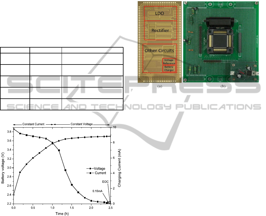
Figure 13: Measured charging profile of Li-ion battery.
The battery is charged under typical Li-ion bat-
tery charging profile. The battery under test is a 3.7V,
20mAh Li-ion battery for implantable devices. It is
charged with 1.2mA and 9.8mA current during trickle
and CC charging regimes respectively. The supply
voltage was set to 4 V,from the LDO. The measured
result of the battery management circuit during the
process of charging is depicted in Figure 13. The
CC, CV and EOC regime are depicted in the Figure
13. As the battery reaches 3.54V the CC regimes
slowly translates to CV regime, driving the OTA into
linear region. In the CV regime, the current slowly
decreases from 9.8mA to 0.15mA based on the tanh
curve. The voltage increases to 3.703 V at the end of
the charging profile. The designed chip unlike prior
design (Do Valle et al., 2011) is bounded to accom-
modate 1 A charging current, without degrading the
stability. The circuit attained about 84% power effi-
ciency at room temperature.
Figure 14: (a) Die micrograph of the chip. (b) Fabricated
chip mounted on socket for testing.
5 CONCLUSION
In this paper, we reported a power efficient design
approach in HV CMOS technology that integrates a
power recovery scheme for WPT system in biomed-
ical implants. The design allows stimulus voltage as
high as 20V and it is four times higher compared to
earlier implementations. The topology is based on
step-down approach and integrated on 2.5mm x 5mm
chip for the purpose of stimulus generation and bat-
tery recharging application. Successful measurement
results indicated that HV regulators can provide sta-
ble output for input variations as high as 30V, and out-
put currents varying from 0.1mA−100mA. The mea-
sured maximum PCE of the rectifier for 2mA load
is determined to be 80.2%. Even though, the design
was focused to protect rectifier from substrate leak-
age current and latch-up at high input voltages and
load currents, the efficiency deviated from the post-
layout simulation results indicate the increased sub-
strate leakage current. However, for typical operat-
ing voltage conditions (15V peak) and load currents
(≤ 2mA), the PCE proved to be effective. The pro-
posed design process supported basic HV transistors
in bulk CMOS process. It limits to achieve desired
results at high input voltages and currents. Further,
case studies and analysis are to be done to decrease
the undesired leakage currents and latch-up in the pro-
posed design. The prototype fabricated is suitable for
biomedical implants.
HighVoltageIntegratedChipPowerRecoveringTopologyforImplantableWirelessBiomedicalDevices
21

ACKNOWLEDGEMENT
This research was supported by Basic Science Re-
search Program through the National Research Foun-
dation of Korea(NRF) funded by the Ministry of
Education(NRF-2013R1A1A4A01012624).
REFERENCES
Balachandran, G. and Barnett, R. (2006). A 110 na volt-
age regulator system with dynamic bandwidth boost-
ing for rfid systems. Solid-State Circuits, IEEE Jour-
nal of, 41(9):2019–2028.
Ballan, H., Declercq, M., and Krummenacher, F. (1994).
Design and optimization of high voltage analog and
digital circuits built in a standard 5v cmos technology.
In IEEE Custom Integrated circuits Conference, pages
574–577.
Cha, H. K., Park, W. T., and Je, M. (2012). A cmos
rectifier with a cross-coupled latched comparator for
wireless power transfer in biomedical applications.
IEEE Transactions on Circuits and Systems-ll:Briefs,
59(7):409–413.
Chen, M. and Rincon-Mora, G. (2006). Accurate, com-
pact, and power-efficient li-ion battery charger circuit.
Circuits and Systems II: Express Briefs, IEEE Trans-
actions on, 53(11):1180–1184.
Do Valle, B., Wentz, C., and Sarpeshkar, R. (2011). An
area and power-efficient analog li-ion battery charger
circuit. Biomedical Circuits and Systems, IEEE Trans-
actions on, 5(2):131–137.
Garimella, A., Furth, P. M., Surkanti, P. R., and Thota, N. R.
(2011). Current buffer compensation topologies for
ldos with improved transient performance. Analog In-
tegr Circ Sig Process, 73(1):131–142.
Guo, S. and Lee, H. (2009). An effiency-enhanced
cmos rectifier with unbalanced-biased comparators
for transcutaneous-powered high-current implants.
IEEE Journal of solid-State Circuits, 44(6):1796–
1804.
Huang, P., Lin, H., and Lin, Y. T. (2006). A simple sub-
threshold cmos voltage reference circuit with channel-
length modulation compensation. IEEE Transactions
on Circuits and Systems II: Express Briefs, 53(9):882–
885.
Lee, H. M. and Ghovanloo, M. (2011). An integrated
power-efficient active rectifier with offset-controlled
high speed comparators for inductively powered ap-
plications. IEEE Transactions on Circuits and Systems
I: Regular Papers, 58(8):1749–1760.
Li, P. and Bashirullah, R. (2007). A wireless power in-
terface for rechargeable battery operated medical im-
plants. Circuits and Systems II: Express Briefs, IEEE
Transactions on, 54(10):912–916.
Li, Y. T., Chang, C. H., Chen, J. J. J., Wang, C. C., and
Liang, C. K. (2005). Development of implantable
wireless biomicrosystem for measuring electrode-
tissue impedance. Journal of Medical and Biological
Engineering,, 25(3):99–105.
Li, Y. T., Peng, C. W., Chen, L. T., Lin, W. S., Chu,
C. H., and Chen, J. J. J. (2013). Application of
implantable wireless biomicrosystem for monitoring
nerve impedance of rat after sciatic nerve injury. IEEE
Transactions on Neural Systems and Rehabilitation
Engineering, 1(21):121–128.
Mandal, S. and Sarpeshkar, R. (2007). Low-power cmos
rectifier design for rfid applications. IEEE Trans-
actions on Circuits and Systems I: Regular Papers,
54(6):1177–1188.
Mouna¨ım, F. and Sawan, M. (2011). Integrated high-
voltage inductive power and data-recovery front end
dedicated to implantable devices. IEEE Transactions
on Bio-Medical Circuits and Systems, 5(3):283–291.
Mounaim, F. and Sawan, M. (2012). Toward a fully in-
tegrated neurostimulator with inductive power recov-
ery front-end. Biomedical Circuits and Systems, IEEE
Transactions on, 6(4):309–318.
Nakamoto, H., Yamazaki, D., Yamamoto, T., Kurata, H.,
Yamada, S., Mukaida, K., Ninomiya, T., Ohkawa, T.,
Masui, S., and Gotoh, K. (2007). A passive uhf rf ide-
tification cmos tag ic using ferroelectric ram in 0.35-
um technology. IEEE Journal of solid-State Circuits,
42(1):101–110.
Nicolson, S. and Phang, K. (2004). Step-up versus step-
down dc/dc converters for rf-powered systems. In
Circuits and Systems, 2004. ISCAS ’04. Proceedings
of the 2004 International Symposium on, volume 5,
pages V–900–V–903 Vol.5.
Rincon-Mora, G. A. and Gabriel, A. (2009). Analog IC
Design With Low-dropout Regulators. McGraw-Hill.
Su, C., Islam, S. K., Zhu, K., and Zuo, L. (2012). A high-
temperature, high-voltage, fast response linear voltage
regulator. Analog Integr Circ Sig Process, 72:405–
417.
Thil, M. A., Gerard, B., Jarvis, J. C., Vince, V., Veraart, C.,
Colin, I. M., and Delbeke, J. (2004). Tissue-electrode
interface changes in the first week after spiral cuff im-
plantation: Preliminary results. In Annual Conference
of the International FES Society.
Tomita, K., Shinoda, R., Kuroda, T., and Ishikuro, H.
(2012). 1-w 3.3 -16.3-v boosting wireless power trans-
fer circuits with vector summing power controller.
IEEE Journal of solid-State Circuits, 47(11):2576–
2585.
Wang, G., Liu, W., Sivaprakasam, M., and Kendir, G. A.
(2005). Design and analysis of an adaptive transcuta-
neous power telemetry for biomedical implants. IEEE
Transactions on Cicuits and Systems-1, 52(10):2109–
2117.
Zou, V. and T, L. (2012). Modeling of substrate leakage
currents in a high-voltage cmos rectifier. Analog In-
tegr Circ Sig Process, 71:231–236.
BIODEVICES2015-InternationalConferenceonBiomedicalElectronicsandDevices
22
