
12 GHz CMOS MEMS Lab-on-chip System for Detection of
Concentration of Suspended Particles in Bio-suspensions
Subhajit Guha, Alexander Wolf, Marco Lisker, Andreas Trusch,
Chafik Meliani and Christian Wenger
IHP, Leibniz Institue of Innovative Microelectronic, Im Technologie Park 25, Frankfurt(Oder), Germany
Keywords: CMOS/MEMS, Lab-on-chip, Biosensor, High Frequency Bio-Sensor, CMOS Biosensor.
Abstract: This work presents a high frequency (X-band) CMOS dielectric sensor with hybrid microfluidic integration,
applied to biosensing techniques; primarily to detect concentration of suspended particles in a solution. The
detection technique is based on capacitive sensing of varying permittivity of the aqueous solution caused by
different concentrations of suspended particles. The sensor chip is fabricated in 0.25 µm SiGe:C BiCMOS
technology of IHP with post processed PDMS microfluidic hybrid integration. The operating frequency of
the sensor is 12.3 GHz and draws a DC power of approximately 35 mW from 3 V power supply. The
dielectric sensitivity of the chip was characterized and calibrated using different organic fluids (alcohols); a
sensitivity of 100 MHz/permittivity was measured with the sensor. After the calibration phase, the sensor
was further used to measure the concentration of glucose in a homogeneous glucose solution. Frequency
down-shift of 250 MHz/10% increase in water concentration in the homogeneous solution was observed. In
order to analyse the concentration of suspended particles in a solution various concentrations of micro-beads
in acetone solution were measured. Approximately a frequency up-shift of 125 MHz/10 µl increase in bead
volume in acetone was observed. The overall chip size is 2.76 mm
2
.
1 INTRODUCTION
Miniaturized sensors applied to biological and
diagnostic purposes have led to approaches where
measurement and analysis of extremely small
volumes of assays are feasible. With the advent of
micro-fabrication technique and its extension to
microfluidic technology, analysis of samples in the
order of few pico litres has become a reality. Such
complex systems are termed as lab-on-chip (LOC)
devices due to high level of miniaturization and also
parallel analysis capabilities, analogous to a state of
the art biotechnology laboratory. However, detection
and sensing technique in such established LOC
devices rely mainly on optical measurement
techniques as explained by Pires et al (2014).
Although optical measurements often provide a
more visually precise result, the measurement
systems are governed by bulky optical devices and
test-benches. Therefore, the advantages of
developing miniaturized LOC devices are no longer
rational. Added to this, optical measurement
techniques require bio-markers, referred as
fluorescent markers and these markers can
additionally alter the properties of the assays.
Therefore, adapting to a label free sensing approach,
based on “all electrical” technique is absolutely
imperative.
Established electrical analysis methods of
biological suspensions rely on static amperometric
techniques or impedance measurements demons-
trated by various research groups like, Goh and Ram
(2010), Krommenhoek et al (2006), Faenza et al
(2012) and Rassaei et al (2012). Usually impedance
measurements are performed at frequency range of
100 KHz to a few MHz as described by
Krommenhoek et al (2006). In this frequency range
(“low frequency”) biological suspensions show
dielectric dispersions based on the properties of
suspended particles, for example cells. Therefore,
measurement and sensing in this frequency regime
are competent for detection of low frequency
properties of suspended particles or cells (for e.g. in
case of cells, membrane capacitance). However, in
order to detect concentration of particles or cells in a
suspension such dispersions can be highly
cumbersome and can lead to falsified measurement
data. Additionally, “low frequency” measurement
techniques also bring in electrode polarization
49
Guha S., Lisker M., Trusch A., Wolf A., Meliani C. and Wenger C..
12 GHz CMOS MEMS Lab-on-chip System for Detection of Concentration of Suspended Particles in Bio-suspensions.
DOI: 10.5220/0005219300490057
In Proceedings of the International Conference on Biomedical Electronics and Devices (BIODEVICES-2015), pages 49-57
ISBN: 978-989-758-071-0
Copyright
c
2015 SCITEPRESS (Science and Technology Publications, Lda.)

mechanism at the electrode electrolyte (biological
suspension) interface, leading to another dispersion
mechanism called the “α dielectric dispersion”,
described by Faenza et al (2012). Also double layer
capacitance at the electrode electrolyte interface
influences the impedance measurement and requires
thorough modelling in order to incorporate its effects
on the measurements. Thus, at lower frequencies,
irrelevant dispersion effects and surface electro-
chemistry have a strong influence, often making
measurement and especially detection of
concentration of suspended particles in a solution
extremely complex. On the other hand,
amperometric techniques allow very precise
measurement but suffer from real miniaturization
issues as a bulky reference electrode is needed for
maintaining solution potential, as can be seen in
approaches like the one described by Rassaei et al
(2012). High frequency (in the order of tens of GHz)
sensors can offer a potential solution to evade the
aforementioned problems. The compatibility of such
sensors with standard CMOS or BiCMOS process
technology would further reduce fabrication costs,
making them highly lucrative for biosensing
approaches.
The advances in RF engineering have led
research groups to explore high frequency
characterization of biological suspensions and
biomaterials. Grenier et al (2013) have demonstrated
the distinction of living and dead cells using
dielectric spectroscopy form 1 GHz to 40 GHz with
a passive interdigitated electrode sensor. Ferrier et al
(2009) have also shown interferometric microwave
sensors for detection of single cells. A coplanar
waveguide approach to characterize yeast cells was
exhibited by Yang et al (2010). However, most of
the aforementioned characterizing sensors are
primarily passive structures realized on PCBs,
therefore, pressing an ever increasing demand for
complete CMOS or BiCMOS sensor system. In
previous works, for e.g. Guha et al (2013), Guha et
al (2014), we have demonstrated C-band to X-band
complete CMOS microwave sensors for dielectric
characterization of glucose solutions, biomaterials
and also imaging of biomaterials. In this work, we
report a complete CMOS/microfluidic system for
dielectric detection of suspended particles in
biological suspensions in the frequency range of 12
GHz. Hybrid integration of the microfluidic system
to the CMOS chip is performed as a post process
step after the chip fabrication. Simultaneous
electrical and optical measurements of suspended
particles in a solution depict close correlation of
both the measurement. The X-band sensor described
in this work aids in avoiding low frequency
dispersion mechanisms described previously. Thus,
concentration of suspended particles can be
unambiguously detected using such a high frequency
sensor approach.
The dielectric sensing is based on capacitive
scaling of an inetrdigitated capacitor (IDC),
embedded in a CMOS cross coupled oscillator,
analogous to a voltage controlled oscillator as
explained by Lee (1998). In this report, the IDC acts
as the variable capacitor. The capacitive scaling
results in shift of resonant frequency of the CMOS
oscillator. Therefore, the change of capacitance
caused by the permittivity variation of the IDC
ambient is read out as the resonant frequency shift of
the oscillator. The permittivity variation is caused by
the dielectric properties of the solutions flowing
within the microfluidic channel aligned on top of the
sensor.
2 SENSOR SYSTEM DESIGN
The complete sensor system design includes a two-
step process. The CMOS dielectric active sensor
chip (CMOS oscillator with the embedded IDC) is
fabricated in the standard 0.25 µm SiGe:C BiCMOS
technology of IHP. The microfluidic system is made
from polydimethylsiloxane (PDMS) using soft
lithography technique with SU8 master mold. The
sensor chip is diced from the wafer and bonded to
the microfluidic system using oxygen plasma
bonding technique.
2.1 Sensor Design
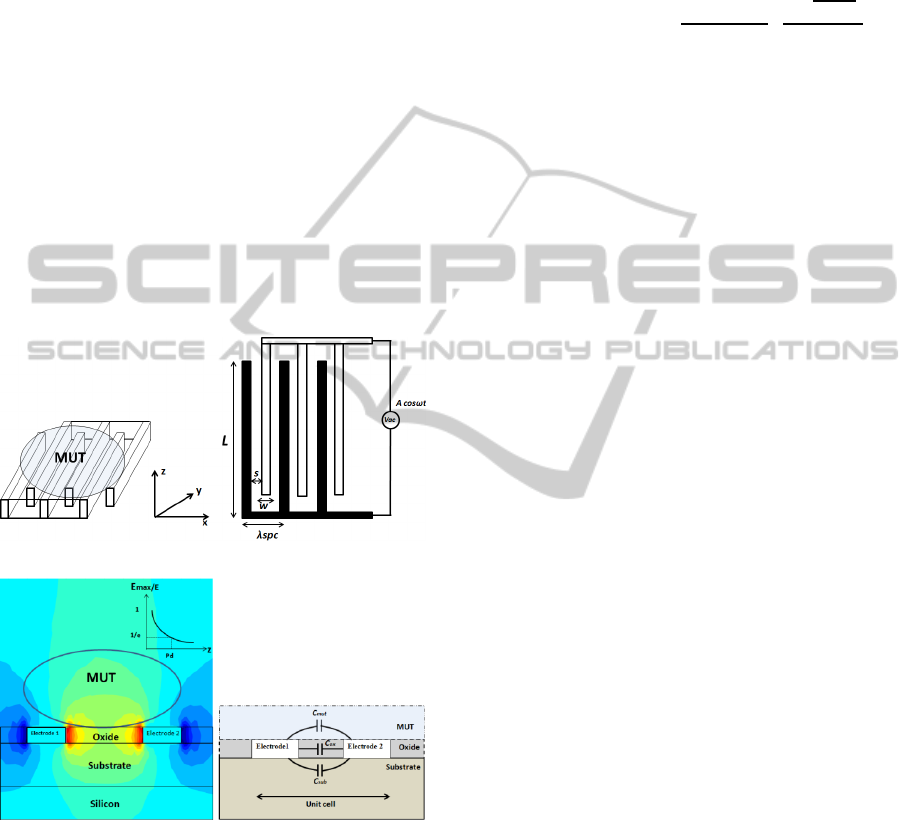
A multi-fingered planar IDC is used as the sensor in
this work. The sensing principle is based on the
variation of fringing electric fields between the
fingers of the IDC, due to the change of permittivity
on top of it. Fig. 1 (a) shows the 3D structure of an
IDC with material under test (MUT) placed on top
of it. The 2D IDC geometry shown in Fig. 1(b)
defines the spatial wavelength of the structure λ
spc
,
which is the distance between two successive fingers
on the same electrode, also given as λ
spc
= 2(w+s). In
this report, the length l of the finger is 50 µm, width
w is 10 µm and the spacing s is 20 µm. The 2D
simulation of a unit cell of the IDC in Fig. 1(c)
shows the electric field patterns between two
adjacent fingers of the IDC penetrating into the
MUT. The permittivity of the MUT influences the
electric fields and also the capacitance of the IDC.
The fringing field capacitance can be analysed based
BIODEVICES2015-InternationalConferenceonBiomedicalElectronicsandDevices
50
on the quasi static approximation of Maxwell’s
equations. Such an approximation can be utilized
when the spatial wavelength (λ
spc
) of the IDC is
comparatively much smaller than the operating
wavelength (λ
em
) of the same. The operating
wavelength is the wavelength of the electromagnetic
wave defined by the frequency (ω=2πf) of operation,
12.3 GHz in our work. Therefore, the spatial
wavelength (λ
spc
= 60 µm) is considerably smaller
compared to the operating wavelength (λ
em
= 2.5
cm), and hence, quasi static approximation of
Maxwell’s equation holds well. The intensity of the
electric field decays exponentially along the z
direction as shown with simulation results in Fig.
1(c). The penetration depth (P
d
) of the electric field
is defined as the distance from the IDC surface along
the z direction, where the strength of the electric
field is 1/e times the maximum field strength. Thus
such a sensor can be effectively used for near field
sensing approaches.
(a) (b)
(c) (d)
Figure 1: (a) 3D structure of IDC with MUT on top. (b)
2D geometry of the IDC. (c) 2D simulation of electric
field in IDC (d) Modelling of IDC showing the different
capacitive contributions.
The total per unit length capacitance of the unit
cell of the IDC is the summation of the capacitive
contributions due to the fringing fields penetrating
into the substrate and the MUT and the parallel plate
capacitive contribution due to the height of the
fingers. The various capacitive contributions are
shown in Fig. 1 (d). The mathematical formulation
of the capacitive contributions can be expressed as,
(1)
The fringing field capacitance per unit length
due to the MUT and substrate is given by,
√
(2)
where, K(k) is the solution of the infinite
elliptical integral dependent on the geometry of the
IDC. The total capacitance of the IDC is given as,
1
(3)
For a given geometry of the sensor, all the other
capacitive contributions being effectively constant,
the fringing field capacitance due to the MUT is the
unique variable, depending on the permittivity of the
MUT. The operating frequency of the sensor
determines the frequency at which the electric fields
within the MUT change their polarity. Thus, the
permittivity of the MUT as sensed by the IDC is
essentially the permittivity at the operating
frequency.
In addition to the geometry, another very
significant parameter of the sensor structure
designed for high-frequency sensing technique is the
self-resonating frequency (SRF) of the structure.
SRF of a structure is defined as the frequency at
which the capacitive contribution of the structure is
nullified by its self-inductive contribution and the
structure is purely resistive. The self-resonating
phenomenon is shown in Fig. 2(a), where the
resonance peak in the capacitance vs. frequency
curve defines the frequency at which the IDC’s self-
inductance nullifies the capacitive contribution. The
SRF is dependent on the size of the sensor and also
on the permittivity of the substrate and the MUT.
For a given geometry of the IDC on a specific
substrate, the SRF is only dependent on the
permittivity of the MUT. With the increase of the
permittivity of the MUT the capacitance of the IDC
increases and the SRF reduces as shown in Fig. 2(a).
It is significant to design the operating frequency of
the sensor system considerably lower than the SRF
of the IDC. Fulfilment of such a condition ensures
that the electric field in the IDC is rotation free and
the structure is essentially capacitive. The simulated
SRF of the IDC structure used in this work is
beyond 150 GHz and the operating frequency of the
oscillator circuit is 12 GHz. Thus, the structure is
purely capacitive in the operating frequency range
and Maxwell’s equation in quasi static
approximation can be applied, as discussed
12GHzCMOSMEMSLab-on-chipSystemforDetectionofConcentrationofSuspendedParticlesinBio-suspensions
51
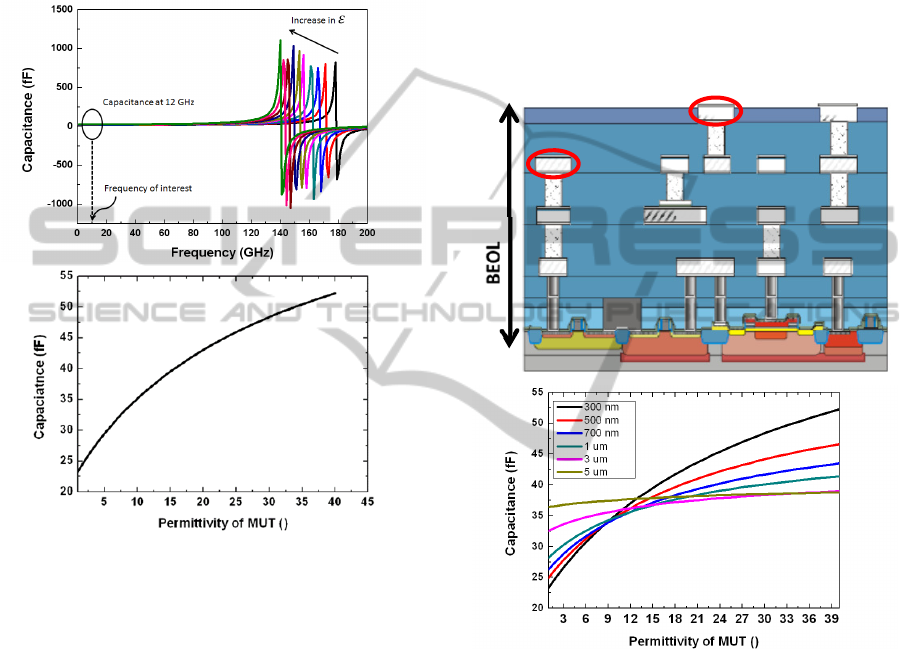
previously. Equation 2 shows that the capacitance of
the IDC increases with increase in the permittivity of
the MUT, and the same is shown in the simulation
results in Fig. 2(b) for the operating frequency
around 12.3 GHz range. With respect to the sensing
mechanism this up-shift of capacitance would be
read out as a downscale of the resonant frequency of
the oscillator.
Figure 2: (a) Impedance simulation of IDC showing
constant capacitance at desired frequency. The self -
resonating frequency is far from the operating frequency.
(b) Variation of capacitance of IDC with permittivity of
MUT.
2.1.1 Fabrication of IDC
The IDC structure along with the CMOS oscillator is
fabricated in the BiCMOS process line of IHP. Fig.
3(a) shows the planarised 0.25 µm SiGe:C BiCMOS
back end of line (BEOL) stack with four metal
layers. The bottom metal layers are lossy due to
relatively small thickness as compared to the two top
metal layers termed as TM1 and TM2. The IDC is
designed in the lower loss TM2 metal layer of the
BiCMOS stack. One major implication of the choice
of the metal layer for designing the IDC, along with
the influence on its quality factor is the influence of
passivation layer. Passivation layer in micro-
fabrication or CMOS technology is an insulation
layer grown on top of the metal layers (electrodes) to
protect the metal layers from external environment.
The passivation layer for a standard BiCMOS
process is 400 nm of Si
3
N
4
(silicon nitride). In this
work, in order to bond the PDMS microfluidic
channel without further fabrication assisted steps,
the standard Si
3
N
4
passivation layer is replaced by
an SiO
2
(silicon dioxide) layer, followed by a
Chemical Mechanical Polishing (CMP)
planarization described by Lisker et al (2013).
Therefore, when the IDC is designed on the topmost
metal layer of the BiCMOS stack, as is done in this
work, the passivation thickness is that of the height
of SiO
2
and has a permittivity of 4.1.
Figure 3: (a) Schematic cross section view of IHP’s
BiCMOS stack. The sensor is fabricated on the topmost
metal layer of the stack. (b) Simulation of variation of
capacitance with permittivity for different thicknesses of
the SiO
2
layer layer.
The thickness and the permittivity of the SiO
2
layer influence the sensor sensitivity. If the IDC is
designed on the TM1 layer of the BiCMOS stack,
the SiO
2
layer has a thickness of approximately 5
µm. This is the combined height of SiO
2
on TM1
and SiO
2
on TM2. Fig. 3(b) shows the simulation of
the influence of thickness of SiO
2
layer on the
variation of capacitance due to permittivity change
of MUT. The sensitivity of the stand-alone IDC is
defined as the change of capacitance per unit change
of permittivity, which is also given by the slope of
the capacitance permittivity curve. The slope as
TM2
TM1
BIODEVICES2015-InternationalConferenceonBiomedicalElectronicsandDevices
52
noted is reduced with the increase in the thickness of
the SiO
2
layer as shown in Fig. 3b. Such a result is
intuitive from the previous section, where the
strength of the electric field was expected to decay
exponentially along the z direction. The effect of
SiO
2
is of wide interest for near field bio sensing, as
often the electrodes are passivated to prevent them
from coming in direct contact with the bio materials.
It is shown with simulations that the sensor is
sensitive up to a passivation thickness of 5 µm and
thus can be efficiently used in near field bio sensing
applications.
2.1.2 Sensor Circuit Design
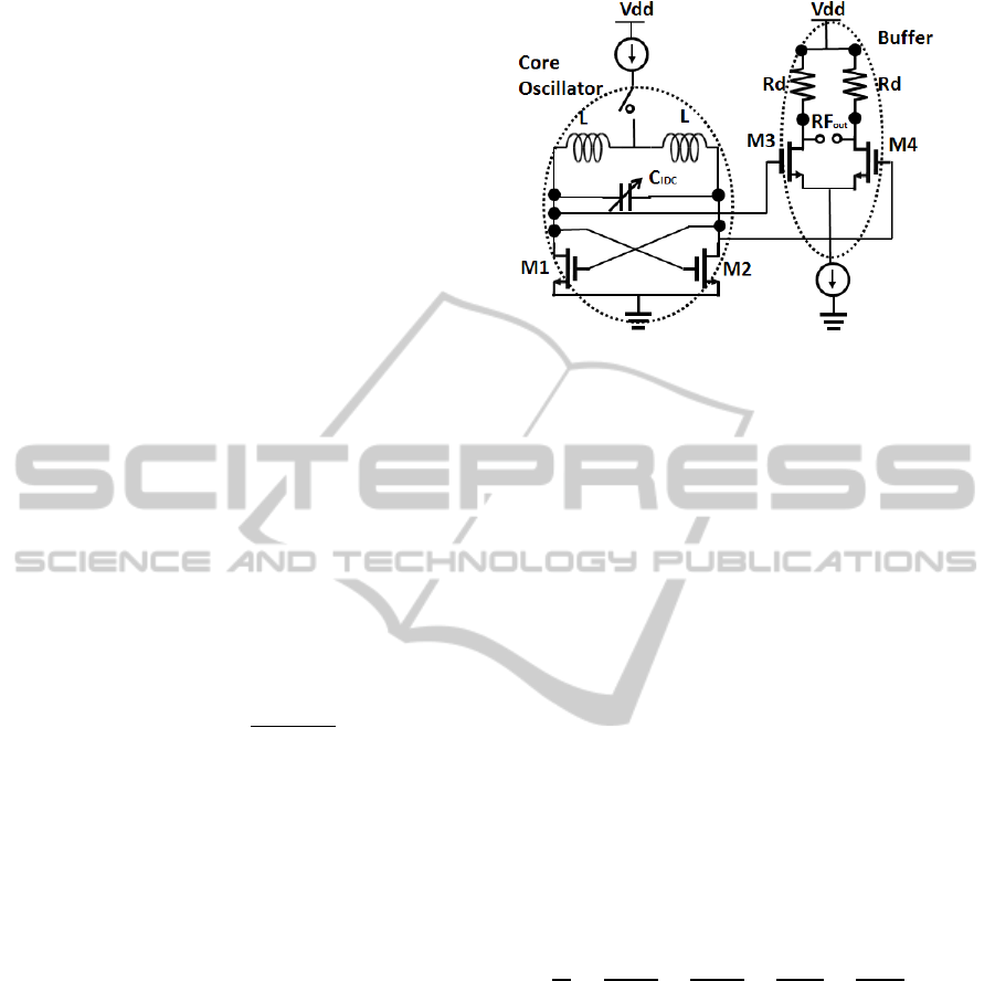
The IDC is coupled with a pair of inductors to form
an LC resonator. The inductor is also fabricated on
the topmost metal layer of the BiCMOS stack
(TM2). The simulated inductance of the inductor is
500 pH, and has a quality factor of approximately 15
at the operating frequency of 12 GHz. The resonant
frequency of the oscillator is the function of the
capacitance of the IDC. The schematic of the
oscillator core with the sensor IDC and the inductors
is shown in Fig. 4. A cross coupled pair of nMOS
transistors drive the oscillation of the resonant LC
oscillator. The resonant frequency of the oscillator
core in the first order approximation is given as
1/2
2
(4)
where, L is the inductance of the individual inductor
and C
total
is the total capacitance of the IDC and the
additional parasitic capacitances due to the
transistors used in the active circuit. The total
capacitance can be mathematically expressed as,
(5)
The parasitic capacitances originate from the cross
coupled transistors driving the oscillations of the LC
resonator tank and also due to the transistors used in
the buffer stage. The buffer stage isolates the
oscillator core from subsequent stages of circuitry.
The parasitic capacitance due to the transistors is
dependent on the size of the transistors. For a
transistor with a greater width of the channel
(w
channel
), the parasitic capacitance is higher due to
the area of the channel. On the other hand the
channel width of the cross coupled nMOS transistors
cannot be made sufficiently small, as wider
transistors are required for sufficient
transconductance (g
m
), to sustain the oscillation of
the oscillator.
The total transconductance of the cross coupled
transistors of the oscillator system nullifies the
Figure 4: CMOS sensor circuit in cross coupled oscillator
topology. The sensor IDC is used as the variable capacitor
in the oscillator.
parasitic resistance of the inductor which would
otherwise result in the damping and eventually dying
of the oscillations. g
m
is directly proportional to the
width of the channel, w
channel
. Hence there exists a
trade-off between the channel width required for
sufficient transconductance of the transistors and the
parasitic capacitance due to the width of the channel.
Parasitic capacitance reduces the sensitivity of the
sensor system as they are in parallel to the sensor
capacitance. For a given transistor size defined for
the sufficient transconductance of the transistor, the
parasitic capacitance is constant which is dependent
only on the width of the transistor. The change of
permittivity due to varied materials on top of the
IDC, would change the C
IDC
contribution of the total
capacitance and in turn change the oscillating
frequency of the oscillator. The sensitivity of the
sensor which is the change of oscillating frequency
with the change of permittivity on top of the IDC
can be mathematically expressed as,
(6)
The output resistance Rd at the buffer stage is 50
ohms in order to match the resistance of the
measuring probes. A standard DC power supply is
used as the source for 3 V V
dd
source as shown in
the circuit schematic. A Rohde and Schwarz X-band
spectrum analyser is used for measurement of the
spectrum.
2.2 CMOS/Microfluidic Integration
PDMS (Polydimethylsiloxane) microfluidic chan-
nels of width 500 µm and height 50 µm was
fabricated using SU8 master mold using soft
lithography technique. The PDMS channel was
12GHzCMOSMEMSLab-on-chipSystemforDetectionofConcentrationofSuspendedParticlesinBio-suspensions
53
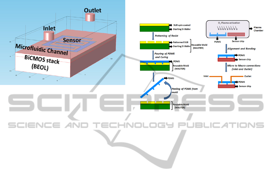
further bonded to the CMOS chip using oxygen
plasma bonding technique. Fig. 5 shows the
schematic view of the CMOS microfluidic system.
Figure 5: Schematic of hybrid CMOS/Microfluidic
dielectric sensor system. The sensor is shown on top of the
BiCMOS BEOL stack. The microfluidic channel is
aligned on top of the sensor.
The BiCMOS wafer was polished using CMP
(Chemical Mechanical planarization) technique to
obtain a planar surface for precise bonding of the
PDMS microfluidic system to the chip.
The master mold was fabricated from SU8
photoresist patterned on a 4 inch silicon wafer. SU8
is most commonly used for such fabrication
techniques because of the capability of producing
high aspect ratio structures with it. PDMS was
prepared using Sylgard 184 Silicone elastomer base
(Monomer) and its curing agent (hardener). The
monomer and the hardener were mixed in the ratio
10:1. Other ratios of monomer to hardener were also
tried for different elasticity of the PDMS structure.
However, the above combination of monomer and
hardener was chosen as it gave the best bonding
strength. After thorough mixing, the solution was
poured on the master mould and cured at a
temperature of 70°C for ninety minutes. Room
temperature curing is also possible but takes a longer
time of approximately a day. The obtained PDMS
structure was carefully peeled off from the mold and
stored in a salinized chamber.
Oxygen plasma bonding of the PDMS
microfluidic channel to the CMOS chip was
performed in the Reactive Ion Etching (RIE)
chamber. Plasma pressure of 16 Pa was used for a
time of 30 seconds with an RF power of 65 Watt.
Using higher RF power reduces the bonding strength
as the PDMS surface which is changed from
hydrophobic to hydrophilic due to the plasma action,
to enable the bonding process, is transformed back
to hydrophobic with higher RF power. Careful
alignment of the channel on top of the sensor was
the limiting factor of the bonding time. The bonding
time was kept within one minute in order to keep the
PDMS in the activated state. Fig. 6 shows the
process steps of the PDMS/CMOS hybrid
microfluidic system.
Figure 6: Fabrication steps of PDMS microfluidic
channels and bonding to the silicon chip. The PDMS
microfluidic channel is bonded to the silicon chip using
oxygen plasma bonder.
3 RESULTS AND DISCUSSION
The silicon chip bonded to the microfluidic system
was measured in two steps. Initially microfluidic
characterization of the chip was performed to check
for leakage of the fluid. Leakage can often occur due
to feeble bonding strength. Leakage of fluid from the
microfluidic channel causes spreading of the fluid on
the bond pads, thus, affecting the probes used for
measurements or damaging the bond wires used for
on board measurements. Therefore, once no leakage
was confirmed, electrical measurements were
performed on a wafer platform for stable
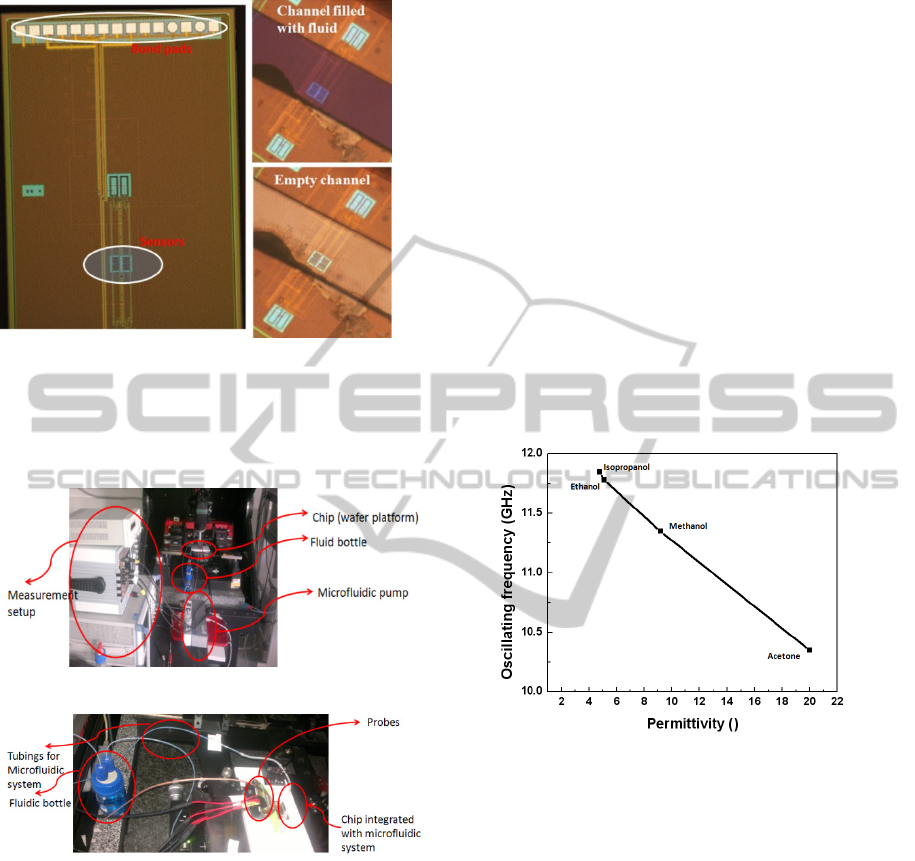
measurements. Fig 7 shows the chip layout and the
microfluidic tests after the hybrid integration of
PDMS microfluidic channel. The channel is aligned
on top of the sensor with the test fluid having no
effect on the inductor coils.
The measurements were conducted in three
steps. Calibration of the sensor was performed using
organic fluids (Alcohols) of known permittivity in
order to establish the sensitivity of the sensor and the
detection limits.
Subsequently glucose solution was measured with
varying concentration of water in the solution and
finally concentration of suspended particles in
acetone was measured. The measurement setup is
shown in Fig. 8
BIODEVICES2015-InternationalConferenceonBiomedicalElectronicsandDevices
54
(a) (b)
Figure 7: (a) Chip layout showing the sensors and the
inductor coils. (b) Microfluidic channel with test fluid in
it. The fluid flows only on top of sensor without
influencing the inductors. (c) Empty microfluidic channel.
(a)
(b)
Figure 8: Measurement setup for the CMOS microfluidic
system. The measurement is performed on the wafer
station, shown in panel a. A DC power supply and a
spectrum analyser is needed for measurement. Panel b
shows the chip with the probes used for the measurement.
3.1 Calibration
The CMOS chips were characterized electrically
prior to microfluidic experiments. The current drawn
by the chip was 12 mA at an operating voltage of 3
V. The oscillating frequency was measured to be
12.32 GHz with an output power of -5 dBm. Further
characterization of the chip was performed after
plasma bonding of the PDMS microfluidic channel
with the chip. The DC operating values of the chip
remained unaltered, while the oscillating frequency
was measured to be 12.20 GHz. The 100 MHz shift
of the oscillating frequency was accounted for the
influence of the PDMS on the inductor coils used in
the design of the oscillator. This resonant frequency
served as the reference for further measurements, as
the microfluidic channel was empty.
The variation of oscillating frequency of the
dielectric sensor with materials of different
permittivities was characterized by using organic
fluids in the microfluidic system. A downshift of
oscillating frequency was observed with increasing
permittivity of the organic fluids, in this case
alcohols. Fig. 9 shows the variation of the resonant
frequency for different alcohols. At 12 GHz
isopropanol and ethanol have almost the same
permittivity (Ɛ= 3.8~4.2), as shown by Belrhiti et al
(2012) and can be seen in the frequency output plot
to be close to each other.
Figure 9: Calibration of sensor with organic fluids. Four
different alcohols with different permittivites at 12 GHz
were measured.
It is also noted that although the static
permittivity of methanol is higher than the static
permittivity of acetone, at 12 GHz, the permittivity
of methanol is less than the permittivity of acetone
described by Kung et al (1997) and the
corresponding shift of resonant frequency shows the
same.
Sensitivity of 100 MHz/permittivity was
observed with the measurements performed with the
organic alcohols. In order to estimate the
measurement reproducibility microfluidic channels
were bonded to five different sensor chips from the
same wafer. Maximum frequency variation of 4
MHz was observed for same measurements and was
negligible compared to the sensitivity of the sensor.
The detection limit of the sensor can also be
estimated with the measurement of isopropanol and
(
c
)
12GHzCMOSMEMSLab-on-chipSystemforDetectionofConcentrationofSuspendedParticlesinBio-suspensions
55
ethanol. The alcohols have a permittivity difference
of 0.7 at 12 GHz and still show a considerable
frequency shift as shown in Fig. 9.
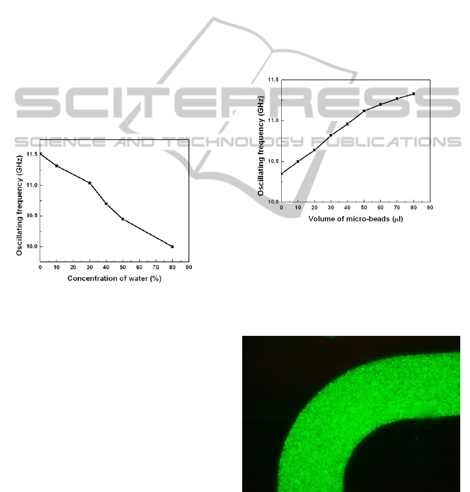
3.2 Glucose Solution Measurement
The CMOS/microfluidic system was then used to
study the effect of water in a homogeneous glucose
solution. The variation of resonant frequency with
different concentration of water depicts the variation
of permittivity of the glucose solution with water
content. Fig 10 shows the downshift of resonant
frequency of the oscillator with increasing water
content. Pure glucose solution has a permittivity of 8
at 12 GHz given by Meriakri et al (2006). The
corresponding oscillating frequency is measured to
be 11.52 GHz. This is close to the value measured
for methanol (Ɛ= 9.2) during calibration. The
obtained results can be extended to determine
permittivity of the glucose solution with different
concentration of water.
Figure 10: Measurement of water content in glucose
solution using the dielectric sensor. The oscillating
frequency down-shifts with increasing water content.
This can be related to the high permittivity of water
at 12 GHz (Ɛ =45). With increasing water content
the permittivity of the overall solution increases. The
downshift of the oscillating frequency indicates an
increase in permittivity with increasing
concentration of water in the glucose solution.
Every 10% increase in the water content shows a
frequency down-shift of 250 MHz, which indicates a
permittivity increase of approximately 2.5.
3.3 Micro-beads Measurement
Concentration of suspended particles in a bio
suspension was emulated with micro-beads in
acetone. Acetone was chosen as it showed the
highest frequency shift during calibration of the
sensor. The influence of micro-beads or particles in
a solution can be understood by the hindrance of
molecular motion given by the Stokes-Einstein
Debye equation described by Basey-Fisher et al
(2011). From the mathematical relation it can be
understood that the characteristic Debye relaxation
time increases or the characteristic frequency
reduces with increasing concentration of particles in
a suspension. In the higher GHz region where γ
dispersion is predominant, the increase in particle
concentration reduces the permittivity of the
solution. In our measurement system we used micro-
beads of diameter 10 µm in different concentrations
in a fixed volume of acetone 2 ml. The beads were
thoroughly mixed in order to prepare a
homogeneous solution.
Figure 11: Measurement of micro-beads in acetone using
the dielectric sensor. The oscillating frequency up-shifts
with increasing concentration of beads.
Fig. 11 shows the variation of the oscillating
frequency with increasing concentration of micro-
beads. This is because the microfluidic channel is
completely filled with the beads after a certain
concentration of beads. This is shown in Fig. 12
Figure 12: Fluorescent marked micro-beads showing the
microfluidic channel being completely filled with the
beads.
BIODEVICES2015-InternationalConferenceonBiomedicalElectronicsandDevices
56

4 CONCLUSIONS
In this work a complete CMOS high frequency
dielectric sensor with hybrid microfluidic integration
was demonstrated. The operating frequency of the
sensor is 12.3 GHz. A sensitivity of 100
MHz/permittivity was measured in the calibration
phase performed with different organic liquids.
Concentration of water in a homogeneous glucose
solution was further measured using the sensor. 250
MHz/10% increase in water content in the glucose
solution was observed. This could be further
interpreted as an approximate increase of 2.5 in the
permittivity of the solution. Concentration of
suspended particles in a solution was further
measured with micro-beads in acetone. Frequency
up-shit of 125 MHz/10 µl increase in bead content in
acetone was measured. All in all a complete CMOS
high frequency sensor with hybrid integrated
microfluidic system was described. The advantages
of using high frequency technique to detect
concentration of particles in a suspension was
investigated and demonstrated in this report.
ACKNOWLEDGEMENTS
The authors would like to thank IHP technology
department for the fabrication of the chip.
REFERENCES
Pires, N.M.M, Dong, T., Hanke, U., Hoivik, N. (2014)
Recent Developments in Optical detection
technologies in Lab-On-a-Chip Devices for
Biosensing Application. Sesnors.14. p. 15458-15479.
Goh, S., and Ram, R.J. (2010) Impedance spectroscopy for
in situ biomass measurements in microbioreactor. 14
th
International conference on Miniaturized Systems and
Life Sciences. Netherlands. p. 1556-1558.
Krommenhoek, E.E., Gardeniers, J., Bomer, J., Van den
Berg, A., Li, X., Ottens, M., van der Wielen, L., van
Dedem, G., Van Leeuwen, M., van Gulik, W.,
Heijnen, J. (2006) Monitoring of yeast cell
concentration using micromachined impedance sensor,
Sensors and Actuators,B. 115.p. 384-389.
Faenza, A., Bocchi, M., Pecorari, N., Franchi, E.,
Guerrieri, R.(2012) Impedance measurement
technique for high sensitivity cell detection in
microstructures with non-uniform conductivity
distribution. Lab Chip 12(11). P.2046-2052.
Rassaei, L., Goluch, E.D., Lemay, S. (2012). Substrate
dependent kinetics in tyrosinase-based biosensing:
Amperometry vs Spectrophotometry. Analytical and
Bioanalytical Chemistry. 493. p.1577-1584.
Grenier, K., Dubuc, D., Chen, T., Artis, F., Chretiennot,
T., Poupot, M., and Fournié, J-J. (2013). Recent
Advances in Microwave-based Dielectric Spectro-
scopy at the Cellular Level for Cancer Investigations
IEEE-TMTT 61(4).p. 2023-2030.
Ferrier, G.A., Romanuik, S.F., Thomson, D.J., Bridges,
G.E., Freeman, M.R. (2009). A microwave interfero-
metric system for simultaneous actuation and detection
of single biological cells. Lab on a Chip. 9. p. 3406-
3412.
Yang, Y., Zhang, H., Zhu, J., Wang, G., Tzeng, T.-R.,
Xuan, X., Huang, K., Wang, P. (2010). Distinguishing
the viability of a single yeast cell with an ultra-
sensitive radio frequency sensor. Lab on a Chip. 10. p.
553-555.
Guha, S., Jamal, F.I., Schmalz, K., Wenger, Ch., Meliani,
Ch. (2013). CMOS lab on a chip device for dielectric
characterization of cell suspensions based on a 6 GHz
Oscillator. European Microwave Conference,
Germany.
Guha, S., Jamal, F.I., Schmalz, K., Wenger, Ch., Meliani,
Ch. (2014) An 8 GHz CMOS Near Field Bio-sensor
Array for Imaging Spatial Permittivity Distribution of
Biomaterials. IEEE MTT-S, Interantional Microwave
Symposium, USA.
T.Lee (1998) The design of CMOS Radio Frequency
Integrated Circuits,Cambridge.
Lisker, M. Trusch, A., Fraschke, M., Kulse, P.,
Borokhovych, Y., Tillack, B., Ostermay, I., Krämer,
T., Schmückle, F.-J., Krüger, O., Krozer, V., Heinrich,
W. (2013). InP-Si BiCMOS Heterointegration Using a
Substrate Transfer Process ECS Transactions.
53(245).
Belrhiti, M.D., Bri, S., Nakheli, A., Haddad, M.,
Mamouni, A. (2012). Dielectric constant determina-
tion of liquid using rectangular waveguide structure
combined with EM simulation. J.Mater.Environ.Sci.
3.p. 575-584.
Kuang, W., Nelson, S.O. (1997). Dielectric relaxation
charcterization of fresh fruits and vegetables from 3 to
20 GHz. J. of Micrwave power and electromagnetic
energy. 32. p. 114-122.
Meriakri, V V., Chigrai, E E., Kim, D., Nikitin, I.P.,
Pangonis, L.I., Parkhomenko, M.P., Won, J.H. (2006).
Dielectric properties of glucose solutions in the
millimetre-wave range and control of glucose content
in blood. IOP, Meas. Sci. Technology. 18.p. 1-6.
Basey-Fisher, T.H., Hanham, S.M., Maier,S.A., Stevens,
M.M., Alford, N.M., Klein, N.( 2011).Microwave
relaxation analysis of Dissolved Proteins:Towards free
solution biosensing. Applied Physics Letters 99.
12GHzCMOSMEMSLab-on-chipSystemforDetectionofConcentrationofSuspendedParticlesinBio-suspensions
57
