
Conceptual Design and Evaluation of a Multichannel ECG Data
Acquisition Device
Mohammadreza Robaei
1
, Yesim Serinagaoglu Dogrusoz
1
and Fikret Küçükdeveci
2
1
Department of Electrical and Electronics Eng., Middle East Technical University, Ankara, Turkey
2
Kardiosis Ltd., METU Teknokent, Ankara, Turkey
Keywords: Electrocardiography, Serial Peripheral Interface, General Purpose Parallel Bus, Recording Unit, Main Unit,
Sub-microcontroller, Main-microcontroller.
Abstract: In this study, we developed a conceptual design for a high resolution multichannel ECG data acquisition
system for recording of electrical activity of the heart. The system has modular architecture, both in
hardware and software layers. It consists of several recording units controlled by sub-microcontrollers, and
one main unit that contains the main-microcontroller. Special distributed message based operating system
has been developed and embedded to sub-microcontrollers and main-microcontroller to provide
communication between them. The operating system is accomplished by the General Purpose Parallel Bus
(GPPB) developed for this design. GPPB is responsible to convey commands, data, addresses, and
handshaking messages. In each recording unit, 8 channels have been sampled by octal simultaneous 24-bit
high resolution ∑-∆ analog-to-digital converter. Sampled data is read out via Serial Peripheral Interface
(SPI) by the corresponding sub-microcontroller. Then, data in the sub-microcontrollers are transferred to the
main-microcontroller using GPPB. At the last step, recorded data is sent from the main-microcontroller to
the computer using USB interface.
1 INTRODUCTION
The goal of electrical imaging of the heart is
extraction and presentation of the electrical activity
of the heart. This can be done either invasively using
catheters, or non-invasively using electrodes
attached to the surface of the body. Recording of the
electrical activity of the heart using electrodes
attached to the surface of the body is called the
electrocardiography (ECG). The most commonly
used ECG system is the conventional 12-lead ECG
system, which records cardiac signals from a limited
number of electrodes on the body surface with
limited resolution. The main advantage that makes
the standard 12-lead ECG the dominant
methodology in clinics is the simplicity and
effectiveness of the method. This method is also fast
enough to be used in emergency situations.
However, ECG has its own restrictions, which force
the researchers to look for replacements. The most
important restriction is the low spatial resolution of
the obtained data, giving inadequate information
about the distribution of the potentials on the surface
of the body. Having adequate amount of information
is essential for several applications such as solving
inverse problem of the heart.
To overcome the low spatial resolution
limitation, either invasive measurements have to be
recorded, or a non-invasive method called the Body
Surface Potential Mapping (BSPM) has to be used.
In BSPM, 32-219 electrodes are attached to both the
anterior and posterior of the torso providing a
greater number of spatial samples (Hoekema, et al.,
1998).
To obtain signals with high spatial resolution
accurately, we need to have a data acquisition
system with the ability to detect small variations of
potential over the torso using tens, or even hundreds
of electrodes attached to the surface of the body.
Like other imaging methods, electrical cardiac
mapping is also a by-product of advances in
electronics and computer sciences. New advances in
highly dense low power CMOS devices and system
architecture techniques make it possible for the data
acquisition system that meet the specifications
appropriately.
In this study it is tried to obey the
recommendations suggested by American Heart
240
Robaei M., Serinagaoglu Dogrusoz Y. and Küçükdeveci F..
Conceptual Design and Evaluation of a Multichannel ECG Data Acquisition Device.
DOI: 10.5220/0005221902400245
In Proceedings of the International Conference on Bio-inspired Systems and Signal Processing (BIOSIGNALS-2015), pages 240-245
ISBN: 978-989-758-069-7
Copyright
c
2015 SCITEPRESS (Science and Technology Publications, Lda.)
Association (AHI) and Association for the
Advancement of Medical Instrument (AAMI)
(Kligfield, et al., 2007). The bandwidth of the
system is between 0.05Hz and 500Hz. Octal,
simultaneous 24-bit Sigma-Delta analog to digital
converter (ADC) is used for sampling of 8-channels
at 1ksps. Digital domain consists of microcontrollers
responsible for control and communication tasks.
Each ADC is supported with a microcontroller,
called sub-microcontrollers, responsible to fire the
sampling and read data through Serial Peripheral
Interface (SPI). After that, data are conveyed to the
main-microprocessor using General Purpose Parallel
Bus (GPPB) developed for this design. Finally, data
are sent to the computer using full speed USB2.0. In
computer, the data is received and stored using
MATLAB for further offline computations.
Our aims of this study can be summarized as: (1)
reporting the technical strategies of design and
implementation of multichannel ECG data
acquisition system, (2) developing an ECG
monitoring device according to new advances in
CMOS and embedded system (3) acquire data for
our group’s works on forward and inverse problems
of ECG.
2 DESIGN ARCHITECTURE
This design consists of four separate parts: (1)
recording units, (2) main unit, (3) power unit, and
(4) backplane.
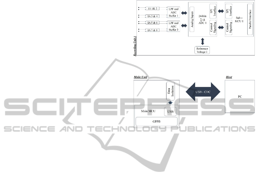
Recording units are responsible to do
measurements from electrodes, amplify, digitize
them, and send them to main unit. All the recording
units function in the same way, and they make their
measurements independently from each other. Each
recording unit is fed by 16 electrodes, which are
used either in bipolar or unipolar mode. In unipolar
mode, recordings are made from just eight
electrodes; however, in bipolar mode, all 16
electrodes are used in pairs. Then, analog signals
from eight channels are converted to digital signals
simultaneously using a Sigma-Delta ADC. Digital
data are transferred from ADC to sub-
microcontroller via SPI, and stored in the sub-
microcontroller. Figure 1 shows the architecture of
an 8-channel recording unit.
The main unit is the core of the design
responsible to manage the device. This unit consists
of main-microcontroller and data isolator. This unit
also sends recorded data to the computer using
USB2.0 interface module integrated in the main
microcontroller. Error! Reference source not
found. shows the main unit and the host, computer.
Figure 1: Recording unit.
Figure 2: Main unit and host.
Data are sent from sub-microcontrollers to main-
microcontrollers using GPPB interface that is
developed for this system. GPPB not only handles
the data transfer from sub- to main-microcontroller,
but also carries commands from main-
microcontroller to sub-microcontrollers. These
commands control the events (data conversion and
SPI, parallel communication, and USB data
transfer).
The system is powered by a battery. The required
power rails are generated in the power unit. The
required voltages are ±5V, +3.3V, and +1.8V. All
these power lines and GPPB are embedded in the
backplane. In addition, backplane carries the
Wilson’s Central terminal implemented in the first
recording unit to all the other units. All working
units are connected to the backplane using DIN
41612 Type R connectors. Figure 3 shows the
backplane and the lines carried by it.
3 DESIGN DETAILS
3.1 Analog Front-End
Analog front-end is the section of the design that
dete cts and amplifies and filters the potentials from
body surface. Error! Reference source not found.
depicts the analog front-end circuitry.
ConceptualDesignandEvaluationofaMultichannelECGDataAcquisitionDevice
241
Figure 3: Backplane carrying GPPB, WCT, and power
rails.
Ag/AgCl electrodes are preferred for their low
half-cell potential values (0.220V). This is important
since half-cell potential can generate dc-offset that
may cause saturation of the amplifier. Analog path
also can cause polarization of the electrodes if sink
current from electrodes. To prevent this effect, op-
amps with high input impedance and low bias
current are used in the input stage.
The measurements are amplified by gain of
13.89 by instrumentation amplifier. The unipolar or
bipolar measurement can be adjust by the jumper at
the input of in-amp as shown in Figure 4. Next, the
analog signals are passed through 500Hz Salen-Key
low pass filter implemented by fully differential
amplifier with unity gain.
3.2 Analog to Digital Conversion
Since we were interested in simultaneous recording,
we selected ADS1278, octal simultaneous 24-bit
Sigma-Delta converter from TI as ADC. This device
provides several flexibilities for conversion type,
interface format, and output format. Four conversion
types are possible: high speed, high resolution, low
speed, and low resolution. It supports two types of
interfaces: Frame-Sync, and SPI, and data can be
read in several format such as discrete or TDM
formats. In prototype design, evaluation module
containing ADS1278 is used. We also use
MSP430F5529LP evaluation board from TI as sub-
microcontroller to read data by 3-wire SPI. The
conversion and data output types are either adjusted
by hardware from ADS1278EVM or by software by
sub-microcontroller. To ensure the proper
functionality of the ADS1278EVM, it was tested
using MMB0 motherboard and ADCPro user
interface both from TI.
Figure 4: Analog path.
3.3 Digital Data
Recorded data is transferred to main-microcontroller
using GPPB to be send to the computer by USB
interface. In this section GPPB, USB and the
embedded operating system that manipulate the
infrastructure are described.
3.3.1 Gppb
GPPB is the interface developed according to the
IEEE488 protocol (ANSI/IEEE, 1988). As shown in
Figure 3, it consists of four distinct buses. Three of
these buses are used for data transfer and one bus is
dedicated to commands. Data are stored in 8-bit
format sub-microcontrollers and main-
microcontroller. For all sub-microcontrollers, the
size of the data buffer is the same (typically 127B).
To have a point-to-point data transfer, the addresses
of the data are sent together with data. The address
determines the cell in main-microcontroller, in
which it is supposed to be stored. Figure 5 shows
this process for a system with one sub-
microcontroller.
Figure 5: Parallel point-to-point data transfer.
For a system with multiple sub-microcontrollers,
address calibration is required to store data in correct
place. This index adjustment is defined by Equation
(1). In this equation, “” 1,2,3,…,32 is the
index of sub-microcontroller, “”
0,1,2,...,127 is the address of data, and “k”
is the new address of data in the main-
BIOSIGNALS2015-InternationalConferenceonBio-inspiredSystemsandSignalProcessing
242
microcontroller. This algorithm prevents data loss
while transferring.
128
1
(1)
Since the parallel interface is asynchronous,
handshaking signals are required to ensure proper
data exchange. Figure 6 shows the operating system
embedded to the sub and main-microcontrollers. It
depicts how the commands, data address, and data
are exchanged using GPPB.
3.3.2 Usb
The integrated USB transceiver of MSP430x5xx
family supports USB 2.0 full-speed (12 Mbps).
Integrated programmable USB Application
Programming Interface (API) together with
Descriptor Tool provide easy data transfer through
USB (Texas Instrument, 2014). In this study
Communication Device Class (CDC) is used for
communication between the device and host
computer.
3.3.3 Operating System
The operating system is the distributed software
embedded in the microcontrollers responsible for
managing of the events. As shown in Figure 6, in
physical layer there are three types of buses
responsible to manipulate the operating system. In
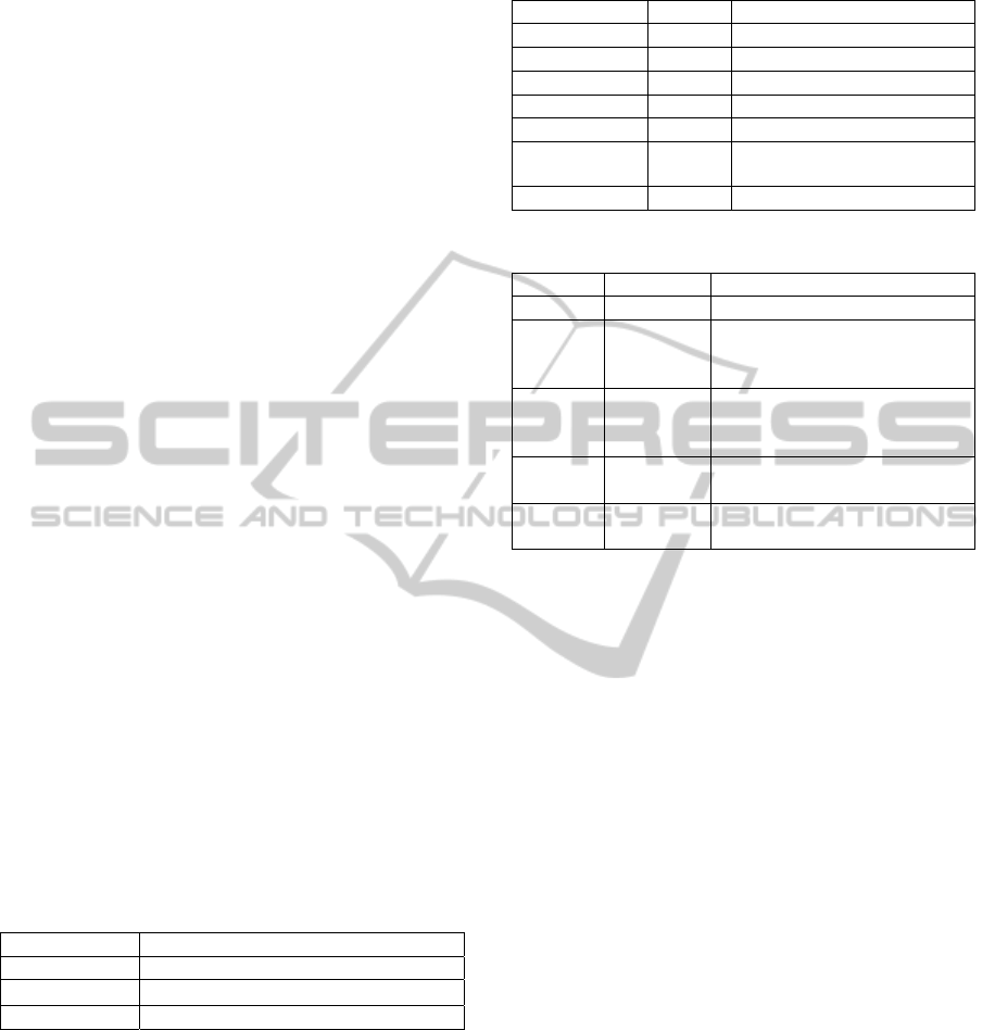
Table 1 buses and their functions are given. Each
event has a distinct code that defines the instruction
and the target of the instruction. For example 0x3F
is SPI command referring to data conversion, and
0x01 is a code for parallel data transfer from sub-
microcontroller. Table2 lists the commands, codes
and the target of the command.
Table 1: Command and data suses.
Bus Function
Command Code define the command
Address 8-bit address of data.
Data 8-bit data
Finally, there are 5 interlocked handshaking
messages responsible of coordination between
events. Three of these handshaking are for
commands and two are for data transfer. Table 3
summarizes the handshaking lines and their
functions. Interlocked handshaking means that the
previous state remains active till the corresponding
handshaking signal is activated. Therefore, the next
command cannot go ahead until the current one has
been completed.
Table 2: Commands, codes, and targets.
Command Code Target
Reset (RST) 0x00 All microcontrollers
SPI 0x3F All sub- microcontrollers
Parallel 0x01 Sub- microcontroller 1
Parallel 0x02 Sub- microcontroller 2
… … …
Parallel 0x20 Sub- microcontroller 32
USB 0xFF Main-microcontroller
Table 3: Command and data handshaking messages.
Message Format Function
CAC1 Command Start and end of the SPI.
CAC2 Command
Start and end of parallel
communication for sub-
microcontroller “n”.
CAC3 Command
Start and end of parallel
communication for all sub-
microcontroller.
DAV Data
Data and address are ready to
be read.
DAC Data
Data and address are read by
main-microcontroller.
4 RESULTS
To have an idea about the feasibility of the
developed concepts, we have done the experiments
using ADS1278EVM and MSP430F5529LP. Our
aim is to have evaluation that proves the workability
of interfaces and codes are used. These interfaces
are: (1) analog-to-digital conversion and SPI, (2)
GPPB, and (3) USB interface. ADS1278EVM
contains the ADS1278 that we plan to use in our
final design. MSP430F5529LP contains the
microcontroller from 5
th
family of MSP430 series
which we plan to use MSP430F5659. The
differences between two devices are mainly in their
memory size and number of I/O pins.
4.1 Spi
In this section two signals are applied to the setup
shown in Figure 7. 8MHz clock is used for
ADS1278EVM and MSP430F5529LP. The
sampling rate is adjusted to 2.66 kHz and data is
gathered in high resolution mode. Input signal is
applied by arbitrary wave generator of Analog
Discovery. The reference voltage is 2.5V, so 1.25V
dc-offset is applied together with both input signals.
In Figure 8 the digitized signal output received and
reconstructed by MATLAB is shown for input signal
ConceptualDesignandEvaluationofaMultichannelECGDataAcquisitionDevice
243
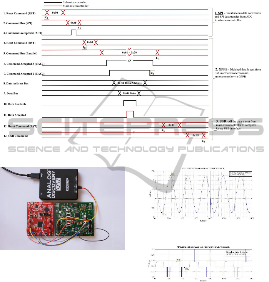
Figure 6: Operating system embedded inside the main-microcontroller. Timing is shown for a system with 32 recording
units. The steps are locked and numbered from 1 to 13 happening one after the other.
Figure 7: Set up used for evaluation of the ADS1278 and
SPI interface.
with amplitude of 2Vp-p and frequency of 1Hz.
Figure 9 is the recovered signal for the square input
with amplitude of 20mVp-p and frequency of 1Hz.
In both figures spikes are obvious in the results
which comes from cables carrying clocks and data.
To eliminate the environmental interference, faraday
cage is recommended.
Figure 8: Recovered 2Vp-p, 1Hz sinusoidal signal from
ADS1278EVM by MATLAB.
Figure 9: Recovered 20mVp-p, 1Hz square signal from
ADS1278EVM by MATLAB.
4.2 Parallel Interface
To simulate the GPPB and its workability two
MSP430F5529LP are used in this section. One of
the boards acts as slave, sub-microcontroller,
sending data through GPPB. The other one acts as
master, main-microcontroller, receiving data via
GPPB. In this way, the workability and the
performance of the parallel data transfer can be
BIOSIGNALS2015-InternationalConferenceonBio-inspiredSystemsandSignalProcessing
244
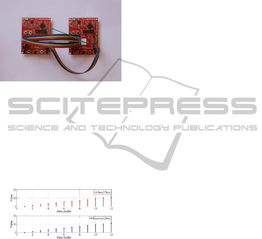
evaluated. The setup used for parallel data transfer is
shown in Figure 10.
Figure 10: Setup used for parallel data evaluation.
For evaluation, data with the size of 12, and
values from 0 to 11 are generated in the slave. These
data are sent from slave to master via GPPB
interface. At the master, data are received and stored
in the buffer defined inside the master. Since data
are sent point-to-point (Figure 6), the received data
have to be the same size and should contain the
same values. To ensure proper execution of this
process, received data are sent to the computer using
the USB interface implemented in master
microcontroller. We expect to have a ramp shaped
data at the final stage. Figure 11 shows the sent data
(red) and the received data (blue).
Figure 11: Parallel data transfer. Signal in red is data sent
by slave (sub-microcontroller) and the figure beneath
shows received data by the master (main-microcontroller).
5 CONCLUSION AND FUTURE
WORKS
In this study the evaluation of the concepts we
developed for multichannel high resolution ECG
data acquisition is considered and experimental
evaluations are made. As it is obvious from Figure 8
and Figure 9, there are spikes at the digital data
received from ADS1278EVM. To solve the spikes,
single PCB containing all stages is an essential. In
addition Faraday Cage is recommended to remove
environmental interferences.
In parallel data transfer and GPPB, just one sub-
microcontroller is used. The timings of the system
(minimum 1ksps) is heavily depended on the
number of sub-microcontroller are used. Further
timing evaluations and improvements are required to
be done in final design. Direct memory access
technique and multi-buffer data storing algorithm
may be required to prevent data loss because of
predicted and unpredicted latencies.
In this paper just one channel is reported;
however, we are working to gather samples from all
the channels simultaneously from multiple ADCs.
Furthermore, for future, additional evaluations
are required to be done on the system performance
such as SNR measurements and analog assessments.
And finally, since this device is aimed to be used
for ECG recording, the experimental results have to
be done to ensure the feasibility of the final product
for ECG application.
REFERENCES
ANSI/IEEE, 1988. IEEE Standard Digital Interface for
Programming Instrumentation, New York: An
American National Standard.
Hoekema, R., Uijen, G. J. H., Stilli,, D. & Van Oosterom,
A., 1998. Lead System Transformation of Body
Surface Map Data. Journal of Electrocardiology,
31(2), pp. 71-82.
Kligfield, P., Childers, R. & et al., 2007.
Recommendations for the Standardization and
Interpretation of the Electrocardiogram Part I: The
Electrocardiogram and Its Technology: A Scientific
Statement From the American Heart Association
Electrocardiography and Arrhythmias Committee,
Council on .... Journal of the American College of
Cardiology, 49(10), pp. 1109-1127.
Texas Instrument, 2014. Programmer’s Guide: MSP430
USB API & Descriptor Tool, s.l.: Texas Instrument.
Texas Instrument, n.d. MSP430Malware: Example codes,
s.l.: Texas Insrument.
ConceptualDesignandEvaluationofaMultichannelECGDataAcquisitionDevice
245
