
Millimetre-wave Electro-Optic Modulator with
Quasi-Phase-Matching Array of Orthogonal-Gap-Embedded
Patch-antennas on Low-k Dielectric Material
Yusuf Nur Wijayanto
1
, Atsushi Kanno
1
, Hiroshi Murata
2
, Sinya Nakajima
1
,
Tetsuya Kawanishi
1
and Yasuyuki Okamura
2
1
National Institute of Information and Communications Technology, 4-2-1 Nukui-Kitamachi, Koganei,
Tokyo, 184-8795, Japan
2
Osaka University, 1-3 Machikaneyama, Toyonaka, Osaka, Japan
Keywords: Electro-optic Modulator, Patch-antenna Array, Quasi-phase-Matching, Low-k Dielectric, Millimetre-wave.
Abstract: In Fibre-Wireless (Fi-Wi) links, conversion devices between wireless microwave/ millimetre-wave and
lightwave signals are required. In this paper, we propose a wireless millimetre-wave-lightwave signal
converter using an electro-optic (EO) modulator with Quasi-Phase-Matching (QPM) array of orthogonal-gap-
embedded patch-antennas on a low-k dielectric material. Wireless millimetre-wave signals can be received
and converted directly to lightwave signals using the proposed device. It can be operated with no external
power supply and extremely-low millimetre-wave losses. The orthogonal-gap-embedded patch-antennas can
be used for receiving dual-linearized or circular polarizations of wireless millimetre-wave signals. The QPM
array structure can be adopted for enhancing modulation efficiency by transit-time effects consideration.
Structure, analysis, and experimental of the proposed device are discussed for 40GHz operational millimetre-
wave bands.
1 INTRODUCTION
Recently, wireless communication has been
implemented and used for transferring data to mobile
devices. Microwave bands are used widely for
carrying data through air medium with several
wireless communication standards such as Wi-Fi,
WiMAX, LTE, and so on (Abichar, 2006) (Akyildiz,
2010). Since demand of high quality data transfers
using mobile devices is always increase time by time,
the microwave bands will be saturated in the near
future. Scientists and researchers are looking for
solving the future problem by minimizing the data,
saving used frequency spectra, enlarging operational
bandwidth, and so on (Mendeiros, 2014) (Lu, 2014)
(Pi, 2011).
In order to enlarge the operational bandwidth,
high operational microwave frequency into
millimetre-wave or sub-millimetre-wave bands are
promising to use for carrying large data with high
transfer speed. The millimetre-wave bands have
relatively large propagation loss in air and metal
cables (Rec. ITU-R P.676-5, 2001) (Iezekiel, 2009).
Therefore, short distance wireless millimetre-wave
communication in pico/ femto-cells can be
developed. Since coverage area of pico/ femto-cells
is small, networking of pico/ femto-cells can be
adopted for enlargement of the coverage area. The
pico/ femto-cell networks can be connected using low
propagation loss optical fibres as backhaul networks
by adopting microwave-photonic technology (Shi,
2011).
Microwave-photonic technology is a combination
technology where microwave and lightwave bands
are operated simultaneously by considering their
advantages such as high mobility, large bandwidth,
no induction, and so on (Seed, 2002). The technology
can be implemented on Fiber-Wireless (Fi-Wi) links
since wireless microwave and optical fibre
communication are used together. In order to realize
the Fi-Wi link, converters between microwave and
lightwave signals are highly required. A high-speed
photo-detector can be used for converting lightwave
signals to microwave signals (Watanabe, 2000). As
the other one, microwave signals can be converted to
lightwave signals by use of a high-speed optical
modulator (Shinada, 2007).
5
Wijayanto Y., Kanno A., Murata H., Nakajima S., Kawanishi T. and Okamura Y..
Millimetre-wave Electro-Optic Modulator with Quasi-Phase-Matching Array of Orthogonal-Gap-Embedded Patch-antennas on Low-k Dielectric Material.
DOI: 10.5220/0005325200050013
In Proceedings of the 3rd International Conference on Photonics, Optics and Laser Technology (PHOTOPTICS-2015), pages 5-13
ISBN: 978-989-758-093-2
Copyright
c
2015 SCITEPRESS (Science and Technology Publications, Lda.)
Generally for wireless applications, a converter from
wireless microwave/ millimetre-wave to lightwave
signals is composed of wireless microwave/
millimetre-wave antennas and optical modulators
(Sheehy, 1993). The antennas are used for receiving
wireless microwave/ millimetre-wave signals. Then,
the received microwave/ millimetre-wave signals are
transferred to the optical modulators by a connection
line, such as a coaxial cable. Therefore, the
microwave/ millimetre-wave signals are modulated
in lightwave signals propagated on optical fibres.
However, microwave/ millimetre-wave signal
distortion and decay might occur in the connection
line when an operational frequency becomes high.
Integration of microwave/ millimetre-wave
antennas and optical modulators fabricated on an
electro-optic (EO) crystal are also developed for
reducing microwave/ millimetre-wave signal
distortion and decay (Bridge, 1991) (Murata, 2012).
They are composed of planar antennas, connection
lines, and resonant electrodes with simple and
compact device structures. Since several microwave/
millimetre-wave planar electrodes on the substrate,
completely impedance matching is required to obtain
effective microwave/ millimetre-wave resonance.
The tuning of them are rather difficult and low
microwave/ millimetre-wave losses might be still
induce along the connection line and their coupling.
New fusion of microwave/ millimetre-wave
antennas and EO modulators were proposed
(Wijayanto, 2011) (Wijayanto, 2012). Patch-antennas
embedded with a narrow-gap were fabricated on EO
crystal as the substrate. Displacement current and
microwave/ millimetre-wave electric field across the
gap can be used for EO modulation. Precise tuning is
not required since only patch-antennas on the
substrate. Therefore, extremely low microwave/
millimetre-wave signal distortion can be achieved
using the fusion structures with a simple and compact
structure. EO modulators using the fusion structures
in an array structure were also reported for enhancing
modulation efficiency by considering transit-time
effect (Yariv, 1989). In high operational frequency,
the patch-antennas becomes small. Therefore,
antenna gain becomes small and microwave/
millimetre-wave-lightwave electric field interaction
length becomes short. The reported devices are
operated effectively for a linear microwave/
millimetre-wave polarization.
In this paper, a millimetre-wave EO modulator
with a quasi-phase-matching (QPM) array of
orthogonal-gap-embedded patch-antennas on a low-k
dielectric material is proposed. By using low-k
dielectric material as an antenna substrate, a large
patch-antenna size can be realized for increasing
antenna gain and enhancing millimetre-wave electric
field strength across the gaps and enlarging
interaction length between millimetre-wave and
lightwave electric fields. Therefore, modulation
efficiency enhancement can be obtained. Further
enhancement of the modulation efficiency can be
achieved using the QPM array structure by
considering transit-time effect. Additionally, the
proposed device can be operated for dual linear or
circular millimetre-wave polarizations.
The device structure, operational principle,
analysis, fabrication, and measurement of the
proposed millimetre-wave EO modulator are
presented for operation with 40GHz millimetre-wave
bands.
2 EO MODULATOR
(a)
(b)
Figure 1: Structure of QPM array of patch-antennas with
orthogonal-gaps on low-k dielectric material stacked with
EO modulator, (a) whole and (b) top views.
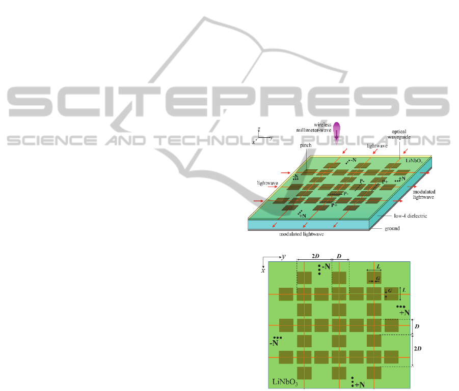
Figure 1 shows a structure of the proposed device.
It consists of a QPM array of patch-antennas with
orthogonal-gaps fabricated on a low-k dielectric
material stacked with a thin LiNbO
3
optical
modulator. The patch electrodes are inserted between
PHOTOPTICS2015-InternationalConferenceonPhotonics,OpticsandLaserTechnology
6
the LiNbO
3
optical crystal and low-k dielectric
material. The patch electrode length, L, is set at a half
wavelength of the designed millimetre-wave. The gap
width, G, is set in micrometre order (<10μm). The
patch electrodes are set in an array structure by
considering a QPM method with a distance of D.
Since a z-cut LiNbO
3
optical crystal is used, optical
waveguides are located on a one side of the gap edge
as shown in cross-sectional view of Figure 2. The gap
position refer to the optical waveguide are slightly
shifted for satisfying the QPM method. A buffer layer
is also inserted between the LiNbO
3
optical crystal
and patch electrodes. The reverse side of the low-k
dielectric material is covered with a ground electrode.
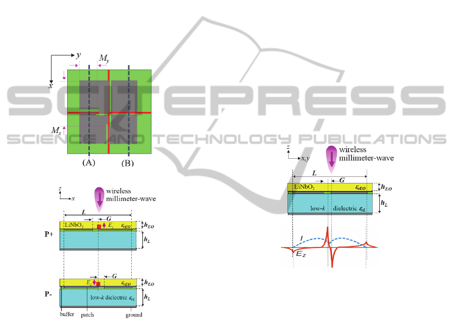
(a)
(b)
Figure 2: Structure of meandering gaps for polarization
inversed structure, (a) top and (b) cross-sectional views.
When a wireless millimetre-wave signal is
irradiated to the device, standing-wave currents are
induced on the patch electrode surface (Lefort, 1997)
(Gupta, 2004). By embedding orthogonal-gaps at the
centre of the patch electrodes, millimetre-wave
displacement current and strong electric field are
induced across the orthogonal-gaps due to current
flow continuity (Rodriguez-Berral, 2011). The
induced millimetre-wave electric field can be used for
optical modulation thru the Pockels EO effect of
LiNbO
3
optical crystal. When lightwave propagating
in the orthogonal optical waveguides located on the
orthogonal-gaps are modulated by the radiated
wireless millimetre-wave signal. Since the gap width
is relatively much smaller than the patch electrode
size, the patch-antenna characteristics are not
changed. Generally, modulation efficiency
improvement can be obtained using an array
structure. However, the spacing between patch
electrodes is required relatively large owing to the
transit-time effect (Yariv, 1989). QPM methods can
be adopted to reduce the spacing of about half.
Therefore, twice modulation efficiency can be
obtained using QPM array structure in the same
device length, since the patch electrodes number
becomes double.
3 ANALYSIS
3.1 Millimetre-wave Analysis
3.1.1 Displacement Current
Figure 3: Millimetre-wave current and electric field profiles
of the proposed device.
When a wireless millimetre-wave signal is
irradiated to the standard patch-antennas with no gap,
a standing-wave millimetre-wave surface current is
induced on the patch electrodes. Then, orthogonal
narrow gaps are introduced at the centre of the patch
electrode as shown in Figure 3. Owing to the
requirement of current continuity on the patch
electrode, millimetre-wave displacement current and
strong electric field are induced across the gap. The
induced millimetre-wave electric field across the gap
is obtained by time integration of the displacement
current. Therefore, it can be expressed as
(
)
=
cos
(
)
(1)
The millimetre-wave current and electric field
profiles of the proposed device are illustrated in
Figure 3.
Millimetre-waveElectro-OpticModulatorwithQuasi-Phase-MatchingArrayofOrthogonal-Gap-EmbeddedPatch-antennas
onLow-kDielectricMaterial
7
3.1.2 Patch-antenna Size
In order to consider for obtaining large antenna gain,
it can be achieved by enlarging patch electrode
fabricated on a low-k dielectric material as the
antenna substrate. In general, a patch electrode size is
inversely proportional to the designed operational
frequency of wireless millimetre-wave signals. It is
also inversely proportional to square root of substrate
effective dielectric constant (Gupta, 2004).
The patch electrode size can be enlarged by
reducing the effective dielectric constant. In order to
reduce the effective dielectric constant of the
substrate, it can be realized using a thin high-k EO
crystal bonded with a low-k dielectric material as
shown in Figure 1. By using a bonded material
structure with a thin EO crystal, the effective
dielectric constant becomes low.
3.1.3 EO Crystal Types
The EO crystal orientation, the distribution of the
millimetre-wave electric field across the orthogonal-
gaps, and position of the optical waveguide must be
taken into account for achieving effective operation.
The orthogonal optical waveguides should be set on
one side of the gap edge as shown in Figure 2, since
a z-cut LiNbO
3
optical crystal is used in the analysis.
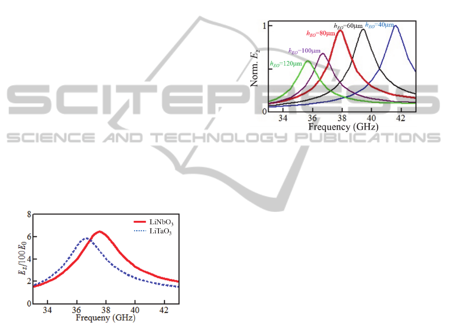
Figure 4: The calculated millimetre-wave electric field
across the gap for z-cut LiNbO
3
(solid-line) and LiTaO
3
(dashed line).
The induced millimetre-wave electric field across
the gaps was calculated using electromagnetic
software analysis. The optical crystal thickness was
set 80μm and low-k dielectric material thickness was
set 130μm with dielectric constant of 3.5. The length
and width of the patch electrodes with gold metal
were set 1.6mm. A gap with 10μm-wide was located
at the centre of the patch electrodes. Ultraviolet
adhesive glue as a buffer layer was also inserted
between the bonded structures. The calculated
electric fields across the gap are shown in Figure 4 for
z-cut LiNbO
3
(solid-line) and LiTaO
3
(dashed line).
The millimetre-wave operational frequencies are
shifted due to different effective dielectric constant of
the devices with bonded structure between
anisotropic LiNbO
3
/ LiTaO
3
crystal and low-k
material. Based on the result, we expected that the
proposed device using z-cut LiNbO
3
crystal can be
used for enhancing modulation efficiency.
3.1.4 EO Crystal Thickness
Figure 5: The calculated millimetre-wave electric field
across the gap for z-cut LiNbO
3
crystal dependences.
Figure 5 shows the calculated millimetre-wave
electric field magnitude across the gap as a function
of operational frequency for several z-cut LiNbO
3
optical crystal thicknesses. The peak frequency is
shifted due to different effective dielectric constant of
the proposed device by changing the LiNbO
3
optical
crystal thickness. When the z-cut LiNbO
3
crystal
thickness becomes thin, operational frequency
becomes high and millimetre-wave electric field
strength becomes large. It is promising also for
obtaining large modulation efficiency.
3.1.5 Millimetre-wave Polarization
Figure 6 shows the calculated electric field
distributions in the z-component for the top view. We
can see that the strong millimetre-wave electric field
is induced across the gaps. The strongest millimetre-
wave electric field is induced when the millimetre-
wave polarization is perpendicular to the gaps.
Almost no millimetre-wave electric field is induced,
when the millimetre-wave polarization is parallel to
the gaps. When the millimetre-wave polarization is
not completely perpendicular or parallel to one of the
gap, the millimetre-wave electric field is induced
across the two orthogonal-gaps. The magnitude of
millimetre-wave electric field across the gap depends
on the millimetre-wave polarization condition.
PHOTOPTICS2015-InternationalConferenceonPhotonics,OpticsandLaserTechnology
8
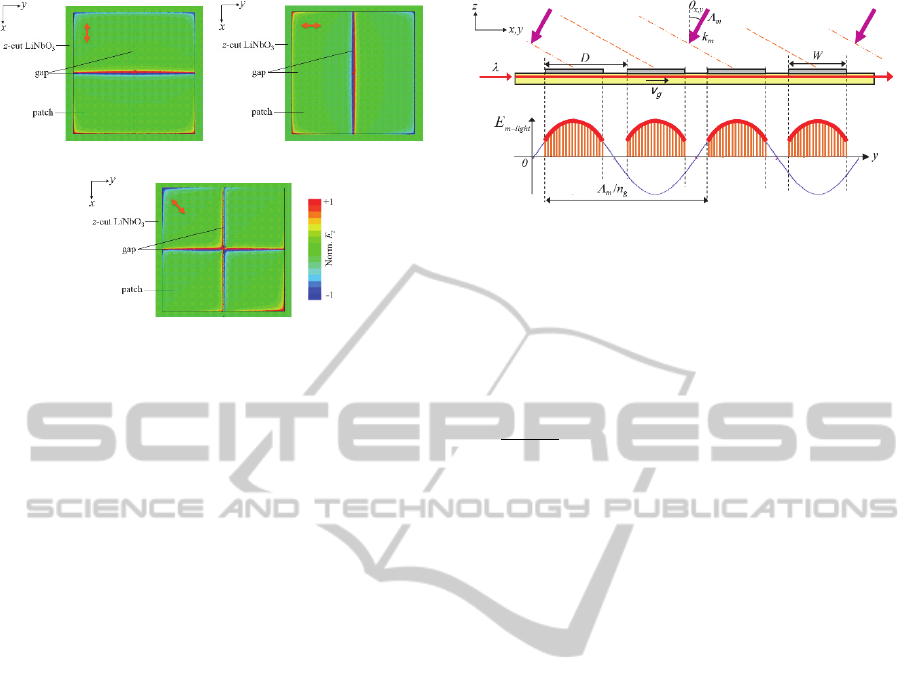
(a)
(b)
(c)
Figure 6: Calculated millimetre-wave electric field
distribution in the z-component for (a) x-, (b) y-, and (c) xy-
polarizations (diagonal).
3.2 Optical Modulation
3.2.1 Transit-time Effect
For an array of gap-embedded patch electrodes, the
temporal phases of the millimetre-wave signal
supplied to the gap-embedded patch electrodes are
changed according their distance, D, and the wireless
irradiation angle,
θ
x
and
θ
y
. When a lightwave
propagates in the optical waveguide, the millimetre-
wave electric field as would be observed by the
lightwave can be expressed by following equation
with taking into account the transit-time of the
lightwave
,
=
cos
+2ℎ(
sin
+)
(2)
where k
m
is the wave number of the millimetre-wave,
n
g
is the group refractive index, h denotes the number
of the gap-embedded patch electrodes, D is a distance
of the patch electrodes (D =
Λ
m
/2n
g
), n
0
is the
refractive index of the millimetre-wave in air (=1),
and
ϕ
is an initial phase of the lightwave (
ϕ
= k
m
n
g
y’). The millimetre-wave electric fields as would be
observed by the lightwave are shown by the
sinusoidal-curve in Figure 7.
The proposed QPM device is an optical phase
modulator, therefore the modulation efficiency,
Δ
φ
from the wireless millimetre-wave signal to the
optical signal is proportional to power ratio between
lightwave carrier and sidebands, when Δ
φ
<< 1. The
modulation efficiency is calculated by the integration
of millimetre-wave electric field as would be
observed by the lightwave along the gap-embedded
Figure 7: Operational principle of QPM EO modulators
under irradiation of a wireless millimetre-wave signal angle
of
θ
x,y
degrees. Modulation efficiency corresponds to the
shaded-areas.
patch electrodes, it can be expressed as following
equation for optical waveguide along y-axis,
Δ(
)
=
Γ()
(,
)
(3)
where
λ
is the wavelength of lightwave propagating
in the optical waveguides, r
33
is the EO coefficient, n
e
is the extraordinary refractive index of the substrate,
Γ is a factor expressing the overlapping between the
induced millimetre-wave and the lightwave electric
field, W are the width of the patch electrodes as the
interaction length of the millimetre-wave and
lightwave electric field, and N is the number of gap-
embedded patch electrodes in an array structure. P(y)
expresses the polarization of the millimetre-wave
electric field in the z-component under the gap edge
along the optical waveguide. The modulation index
of the QPM structure corresponds to the sum of the
shaded areas of the millimetre-wave electric field
observed by lightwave in Figure 7. Since the
modulation index is also a function of wireless
irradiation angle,
θ
, the directivity in the modulation
efficiency can be also calculated using Equation (3).
3.2.2 QPM Array
The millimetre-wave electric fields in the z-
component between two-edges of gaps have different
polarities (Rodriguez-Berral, 2011). The different
polarities enable us to obtain the polarization-
inversed structure for the QPM condition. The
polarization-inversed structures on a z-cut EO
crystals are obtainable by switching spatial
relationship between the gap edge and optical
waveguide along the gap-embedded patch electrodes.
In order to obtain polarization-inversed structure,
meandering gaps can be adopted as shown in Figure
Millimetre-waveElectro-OpticModulatorwithQuasi-Phase-MatchingArrayofOrthogonal-Gap-EmbeddedPatch-antennas
onLow-kDielectricMaterial
9
2. The gaps are meandered on straight optical
waveguide by considering transit-time effect.
Therefore, it can be used for recovering optical
modulation degradation due to miss-matching
between millimetre-wave and lightwave electric
fields.
3.2.3 Wireless Irradiation Angle
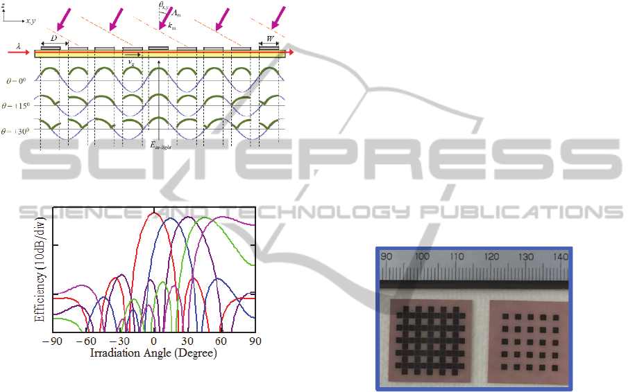
Figure 8: Typical patterns of patch electrodes with
meandering gaps.
Figure 9: Calculated irradiation angle dependence of the
designed QPM EO modulator for several patterns of
meandering-gaps.
The meandering-gaps are promising for wireless
irradiation angle or beam-forming controls. Several
patterns of meandering gaps are designed as shown in
Figure 8. The designed meandering gaps are set by
considering transit-time effect for receiving several
irradiation angles of wireless signals.
The directivity of wireless millimetre-wave
signals in the proposed device can be calculated using
Equation (3). The calculated directivities in the
designed device for several patterns of meandering
gaps are shown in Figure 9. Clearly, the meandering
gaps can be used for controlling irradiation angle or
beam-forming of wireless millimetre-wave signals.
4 EXPERIMENT
4.1 Fabrication Process
The designed device was fabricated. First, a z-cut
LiNbO
3
crystal with a thickness of 250μm was
prepared. Then, single-mode orthogonal channel
optical waveguides were fabricated on the EO crystal
using titanium diffusion method (Hu, 2010). The
titanium were diffused with 1100
0
C for 10 hours.
After that, a 0.2μm-thick SiO
2
buffer layer was
deposited on the EO crystal. An array of patch
electrodes embedded with orthogonal-gaps was also
fabricated on the EO crystal. The patch electrodes
were fabricated using a 2μm-thick gold film on the
EO crystal through thermal vapor deposition,
standard photo-lithography, and a lift-off technique.
The optical waveguides were aligned onto one side of
the gap edge.
A ground metal was deposited to the bottom
surface of a low-k dielectric material. Then, the top
surface of a low-k dielectric material was covered
with an optical adhesive for next bonding process.
Figure 10: A photograph of the fabricated devices with an
array of gap-embedded patch-antennas, (a) with QPM
structures and (b) with no QPM structure.
In bonding process, the EO crystal was flipped
over with 180 degrees. So as the metal antennas
become on the bottom surface of the EO crystal.
Then, the flipped EO crystal was bonded to the low-k
dielectric material by exposing ultraviolet (UV) light
to the UV-cured optical adhesive (Uddin, 2006).
Finally, the 250μm-thick EO crystal was polished to
the designed thickness of 80μm using a polishing
machine with diamond slurry. A photograph of the
fabricated device is shown in Figure 10.
PHOTOPTICS2015-InternationalConferenceonPhotonics,OpticsandLaserTechnology
10
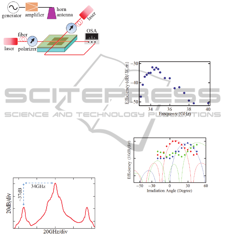
4.2 Measurement Setup
Figure 11: Measurement setup for characterization of the
fabricated devices.
Performance of the fabricated device were
measured experimentally with a measurement setup
as shown in Figure 11. Lights of 1.55μm wavelength
from laser were propagated to optical fibres and
coupled to the fabricated device. Millimetre-wave
signal in 40GHz bands from a signal generator was
amplified and irradiated to the fabricated device using
a horn antenna with an irradiation power of 20mW.
The output lightwave signals were measured using an
optical spectrum analyser (OSA).
Typical of the measured output light spectra from
two orthogonal waveguides are shown in Figure 12,
where a 34GHz wireless millimetre-wave signal was
irradiated at the device at a normal irradiation angle
and polarization of 45 degree. The optical sidebands
were observed clearly. The intensity ratio between the
sidebands and optical carrier were about 37dB.
Figure 12: Typical measured output light spectra from the
orthogonal waveguides.
The measured modulation efficiency as a function
of millimetre-wave frequency is shown by the dots in
Figure 13, when the irradiation angle of the wireless
millimetre-wave signal was set to be normal to the
device. The unit is expressed for power ratio between
carrier and sidebands per millimetre-wave irradiation
power and distance between the horn antenna and
fabricated device. The measured peak frequency was
about 34GHz. It is slightly shifted than the designed
operational frequency due to fabrication error such as
EO crystal thickness, UV-adhesive glue thickness,
and other parameters.
The dots in Figure 14 show the measured
modulation efficiency as a function of wireless
irradiation angle in the yz-plane, when the frequency
of the wireless millimetre-wave signal was set at
34GHz. The largest modulation efficiency for certain
wireless irradiation angle depends on meandering-
gap patterns. The measured directivities are in good
agreement with the calculation results.
Figure 13: Measured modulation efficiency as a function of
the millimetre-wave operational frequency.
Figure 14: Measured modulation efficiency as a function of
wireless millimetre-wave irradiation angles.
5 CONCLUSIONS
Optical modulators with a QPM array of orthogonal-
gap-embedded patch-antennas on a low-k dielectric
material were proposed. A wireless millimetre-wave
signal can be received and converted directly to a
lightwave signal with the proposed device through
EO modulation using the Pockels effect. Performance
of the proposed device for operation in the
millimetre-wave band was demonstrated
experimentally. The proposed device can be operated
for dual linear polarization or circular polarization of
wireless millimetre-wave signals since orthogonal-
gaps are used. Double modulation efficiency can be
Millimetre-waveElectro-OpticModulatorwithQuasi-Phase-MatchingArrayofOrthogonal-Gap-EmbeddedPatch-antennas
onLow-kDielectricMaterial
11

obtained also since a QPM array structure is used.
The proposed device has a compact structure and can
be operated with a low millimetre-wave signal loss
and no external electrical power supply.
The proposed device is promising for broadband
wireless communication such as for Multi-Input
Multi-Output (MIMO) and Space-Division-
Multiplexing-Access (SDMA) (Wijayanto, 2013). It
can be used also for precise measurement/ sensing
applications such as high-frequency Electromagnetic
Compatibility (EMC) chamber and Radio Detecting
and Ranging (RADAR).
ACKNOWLEDGEMENTS
The authors would like thank to Dr. T. Umezawa
from National Institute of Information and
Communication Technology (NICT) Japan and Dr.
H. Shiomi from Osaka University Japan for their
constructive comments and suggestions during
discussion. Thanks to Dr. Y. Ogawa from NICT
Japan for his helpful supports during device
fabrication.
Y. N. Wijayanto, A. Kanno, S. Nakajima, and T.
Kawanishi would like thank to the Ministry of
Internal Affairs and Communications, Japan, for the
financial support partly thru the project entitled
“Research and Development of high-precision
imaging technology using 90 GHz band linear cells”
funded by the “Research and Development to Expand
Radio Frequency Resources.”
REFERENCES
Abichar, Z., Peng, Y., and Chang, J., “WiMAX: The
Emergence of Wireless Broadband,” IEEE Computer
Society, Vols. July-August, pp. 44-48, 2006.
Akyildiz, I. F., Gutierrez-Estevez, D.M., Reyes, E.C., “The
evolution to 4G cellular systems: LTE-Advanced,”
Physical Communication, vol. 3, pp. 217-244, 2010.
Bridges, W. B., Sheehy, F.T., and Schaffner, J.H., “Wave-
Coupled LiNbO
3
Modulator for Microwave and
Millimeter-Wave Modulation,” IEEE Photonics
Technology Letters, vol.3, no.2, pp.133-135, February
1991.
Gupta, V. R. and Gupta, N., “Characteristics of a Compact
Microstrip Antenna,” Microwave and Optical
Technology Letters, vol.40, no.2, pp.158-160, January
2004.
Hu, H., Ricken, R., Sohler, W., "Low-loss ridge
waveguides on lithium niobate fabricated by local
diffusion doping with titanium," Applied Physics B,
vol.98, pp.677–679, 2010.
Iezekiel, S., Microwave photonics: Devices and
Applications, John Wiley & Sons Ltd, Chichester, UK,
2009.
Lefort, G., and Razban, T., “Microstrip Antennas Printed
on Lithium Niobate Substrate,” Electronics Letters,
vol.33 no.9, pp.726-727, April 1997.
Lu, X., Wang, P., Niyato, D., and Hossain, E., “Dynamic
Spectrum Access in Cognitive Radio Networks with RF
Energy Harvesting,” IEEE Wireless Communications,
pp. 102-110, Jun. 2014.
Mendeiros, H. P., Maciel, M. C., Sauza, R. D., and Pellenz,
M.E., “Lightweight Data Compression in Wireless
Sensor Networks Using Human Coding,” International
Journal of Distributed Sensor Networks, vol. 2014, ID
672921, Jan. 2014.
Murata, H., Miyanaka, R., and Okamura, Y., “Wireless
Space-Division-Multiplexed Signal Discrimination
Device Using Electro-Optic Modulator with Antenna-
Coupled Electrodes and Polarization-Reversed
Sructures,” International Journal of Microwave and
Wireless Technologies, vol.4, pp.399-405, April 2012.
Pi, Z. and Khan, F., “An introduction to millieter-wave
mobile broadband systems,” IEEE Communications
Magazine, vol. June 2011, pp. 101-107, 2011.
Recsi. ITU-R P.676-5, “Attenuation of atmospheric gases,”
2001.
Rodriguez-Berral, R., Mesa, F., and Jackson, D. R., “Gap
Discontinuity in Microstrip Lines: An Accurate Semi
analytical Formulation,” IEEE Transactions on
Microwave Theory and Techniques, vol.59, no.6, pp,
1441-1453, June 2011.
Shi, J., Huang, C., and Pan, C., “Millimeter-wave photonic
wireless links for very high data rate communication,”
NPG Asia Materials, vol.3, pp.41, April 2011.
Seeds, A. J., “Microwave Photonics,” IEEE Transactions
on Microwave Theory and Techniques, vol.50, no.3,
pp.877-887, March 2002.
Shinada, S., Kawanishi, T., and Izutsu, M., “A Resonant
Type LiNbO
3
Optical Modulator Array with Micro-
Strip Antennas,” IEICE Transactions on Electronics,
vol.E90-C, no.5, pp.1090-1095, May 2007.
Sheehy, F. T., Bridges, W. B., and Schaffner, J. H., “60
GHz and 94 GHz Antenna-Coupled LiNbO
3
Electrooptic Modulators,” IEEE Photonics Technology
Letters, vol.5, no.3, pp.307-310, March 1993.
Uddin, M. A., Chan, H. P., Tsun, T. O., and Chan, Y. C.,
"Uneven Curing Induced Interfacial Delamination of
UV Adhesive-Bonded Fiber Array in V-Groove for
Photonic Packaging," Journal of Lightwave
Technology, vol.24, no.3, pp.1342-1349, March 2006.
Watanabe, I., Nakata, T., Tsuji, M., Makita, K, Torikai, T.,
and Taguchi, K., “High-Speed, High-Reliability Planar-
Structure Superlattice Avalanche Photodiodes for 10-
Gb/s Optical Receivers,” Journal of Lightwave
Technology, vol.18, no.12, pp. 2200- 2207, December
2000.
Wijayanto, Y. N., Murata, H., and Okamura, Y., “Novel
Electro-Optic Microwave-Lightwave Converters
Utilizing a Patch-antenna Embedded with a Narrow
PHOTOPTICS2015-InternationalConferenceonPhotonics,OpticsandLaserTechnology
12

Gap,” IEICE Electronics Express, vol.8, no.7, pp.491-
497, April 2011.
Wijayanto, Y. N., Murata, H., Kawanishi, T., and Okamura,
Y., “X-Cut LiNbO
3
Optical Modulators Using Gap-
Embedded Patch-Antennas for Wireless-Over-Fiber
Systems,” Advances in Optical Technologies, vol.
2012, Article ID 383212, 8 pages, 2012.
Wijayanto, Y. N., Murata, H., and Okamura, Y., "Electro-
Optic Beam Forming Device Using a Two-
Dimensional Array of Patch-Antennas Embedded with
Orthogonal-Gaps for Millimeter-Wave Signals," IEEE
Photonic Conference 2013, Seattle, 2013.
Yariv, A., Quantum Electronics, 3rd ed., Wiley, New York,
1989.
Millimetre-waveElectro-OpticModulatorwithQuasi-Phase-MatchingArrayofOrthogonal-Gap-EmbeddedPatch-antennas
onLow-kDielectricMaterial
13
