
Creating AlGaAs Photodetectors
O. Rabinovich, S. Didenko, S. Legotin and M. Basalevskiy
National University of Science and Technology “MISiS”, P.O. Box 409, 119313, Russian Federatation
Keywords: AlGaAs, Photodiode, Photodetector, Dark Current, Scintillators.
Abstract: AlGaAs/GaAs photodetectors operate at room temperature in the visible spectrum. Distinctive features of
the photodetectors are: high absolute spectral sensitivity up to 0.112 A / W at λ
max
= 530-570 nm;
photodiodes showed the low dark current of 4.7 nA and 530 nA, accordantly, at 5 V reverse bias. The shift
of the spectral characteristics which is associated with an increase in the band gap was detected.
1 INTRODUCTION
Photodetectors for the visible spectral range can be
used as photodetectors in scintillation counters in
experiments with space rays in neutrino physics, in
experiments with particle accelerators, etc. Getting
information about the particles that came to Earth
from space, is an important research task. For
example, the fastest accelerator allows getting the
particles energy about 10
13
eV, while the energy of
the particles arrived from outer space, can reach
10
17
-10
19
eV. Also due to the sensitivity lack in the
infrared range and high sensitivity in the visible
region, such photodetectors may be used, for
example to control the liquid crystal display (LCDs)
backlight.
Scintillation detector consists of a scintillator
which emits photons when struck by ionizing
radiation and a photodetector that converts light
from the scintillator into an electrical signal. In
present-time detectors optical fibers are used to
improve light focusing from the scintillator.
Typically, the scintillators used for experiments in
high energy physics, emit at a maximum wavelength
λ
max
from 375 to 430 nm. For detection of it light
photomultiplier tubes (PMT) are used because their
maximum spectral sensitivity is almost perfectly
matches the maximum of emission spectrum of
scintillator. But PMT has some disadvantages, that is
why, nowadays, researchers and engineers are
working on finding an alternative to replace the
PMT. The most common alternative is silicon
p-i-n diode (Ryzhikov and Kozin D et al., 2003) or
silicon PMT (SiPM) (Patent RF, 2005; Herbert and
D’Ascenzo et al, 2006; Bloser and Legere et al.
2014).
AlGaAs solid state solutions are high promising
to create photodetectors for this spectral range. Si
has maximum sensitivity about 900 nm, GaAs –
about 800 nm, but by adding Al it can be achieved
high sensitivity in the visible region (400-500 nm)
due to increased bandgap. During the photodetectors
creation it has been assumed that scintillation plate
type SC-301 with maximum in the emission
spectrum about 420 nm is used. To improve the light
focusing optical fibers are used. The wavelength of
transferred light to photodetector is approximately
476 nm.
In this paper photodetectors AlGaAs / GaAs for
detecting light from the scintillator are presented. On
the basis of heterostructures using the standard
contact photolithography photodiodes were
produced (tabl. 1).
Details of the construction and growth method of
these structures are described in (Bloser and Legere.
2014; Murashev and Legotin et al. 2014; Bazalevsky
and Didenko et al. 2014; Legotin and Murashov et
al. 2014; Baryshnikov and Didenko et al. 2012;
Koltsov and Didenko, et al. 2012; Legotin and
Rabinovich et al. 2014). Photodiodes circular Mesa,
the chip size of 4 x 4 mm and a photosensitive
window diameter of 1.5 mm have been mounted in
the housing type TO-39.
87
Rabinovich O., Didenko S., Legotin S. and Basalevskiy M..
Creating AlGaAs Photodetectors.
DOI: 10.5220/0005334100870089
In Proceedings of the 3rd International Conference on Photonics, Optics and Laser Technology (PHOTOPTICS-2015), pages 87-89
ISBN: 978-989-758-093-2
Copyright
c
2015 SCITEPRESS (Science and Technology Publications, Lda.)

Table 1: Basic structure for photodiode.
Layer’s title
Concentration,
(cm
-3
)
Layer’s
width, (nm)
Contact layer, p
+
GaAs
(Be)
2 x 10
18
45
“Window” p
+
AlAs (Be)
2 x 10
18
50
pAl
0.35
Ga
0.65
As(Be)
2 x 10
17
500
nAl
0.35
Ga
0.65
As(Si)
2 x 10
17
500
Buffer n
+
GaAs (Si)
1.5 x 10
18
200
Substrate n
+
GaAs(Si)
1.5 x 10
18
400 μm
2 RESULTS AND DISCUSSION
Schematic cross-sections of finished devices are
shown in figure 1.
Figure 1: Cross section for photodiode.
Dark current and breakdown voltage were measured
by Agilent B1500A semiconductor device analyzer.
Reverse current–voltage characteristic (I-V) of
photodiode is presented in Figure 2. The best
samples demonstrated the dark current I
d
= 3.38 nA
at a reverse bias U
rev
= 5 V. I-V control was carried
out at each stage of devices production, from cutting
wafers into chips till the packaging process (Fig. 3).
The measurements showed that after all
production steps the dark current increased and the
breakdown voltage decreased insignificantly
(Fig. 3).
Calculations of spectral response were carried
out for a p-i-n GaAs structure. It consists of a 0.82
microns thick top p-GaAs layer doped to 5·10
17
cm
-
3
; 45 microns thick i-GaAs region with electron
density 1·10
14
cm
-3
and heavily doped n
+
-substrate
from the back side of the structure. Surface
recombination rate was taken as 2·10
6
cm/s. Figure 4
shows a spectral response of described structure. For
clarity contribution of different regions is shown.
Figure 2: Reverse photodiode I-V characteristic.
Figure 3: Photodiode I-V at wafer and after packaging.
Figure 4: Calculated spectral response of p-i-n GaAs
structure.
Figure 5 shows that the photosensitivity of the
structure from the short-wave edge is determined by
electrons in p-region, and from the long-wavelength
edge by charge carriers generated in the depletion
region and holes in the lightly doped i-region. Thus
blue-shift of spectral response can be achieved by
reducing surface recombination rate and by
increasing mobility and lifetime of electrons in p-
region. Also modeling of p-i-n heterostructure with
PHOTOPTICS2015-InternationalConferenceonPhotonics,OpticsandLaserTechnology
88
p Al
x
Ga
1-x
As layer was performed.
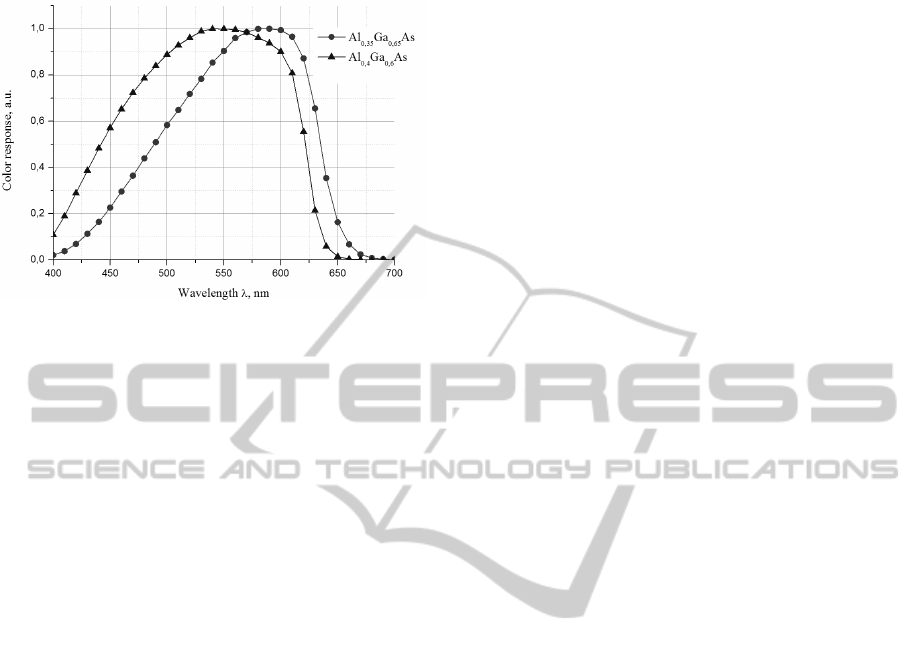
Figure 5: Photodiodes spectral characteristics.
Calculated spectral characteristics are shifted to the
short-wave range and overall sensitivity increases.
At the same time it could be seen that the greatest
increase in sensitivity at wavelengths less than 0.4
microns takes place not for the widest bandgap
material. Someone can find it strange, but the fact is
that in the more wide bandgap-materials the electron
mobility decreases sharply (from 3.1·10
3
cm
2
/V·s for
Al
0.25
Ga
0.75
As to 5.4·10
2
cm
2
/V·s for
Al
0.419
Ga
0.581
As) for the same surface recombination
rate and lifetime of charge carriers.
Spectral characteristics were measured using a
monochromator MDP and apparatus for measuring
the spectral sensitivity of photodetectors
TTM3.435.088. Figure 5 shows the relative spectral
characteristics of the photodiodes.
It’s seen that, at changing the Al mole fraction by
0.05, maximum of spectral sensitivity was shifted by
40 nm to shorter wavelengths. At the same time the
sensitivity at a wavelength of 475 nm was increased
almost twice by choosing the optimum composition
and thickness of the active p-layer. To achieve
greater sensitivity in shorter wavelengths for
photodiodes antireflection coating on “window”
layer will be used.
Photodetectors created for detecting light from
the scintillator based on AlGaAs/GaAs
heterostructures were produced. Photodetectors
measurements showed the low dark current at the
level of 0.5 nA for phototransistors and 10 nA for
photodiodes, for at the same time high breakdown
voltage was about 600 V and 20 V, accordantly.
Experimentally determined values of
composition and thickness for the Al
x
Ga
1-x
As solid
solution allowed to increase the sensitivity almost
twice from 40 to 75 % at a wavelength 475 nm.
Absolute spectral sensitivity of photodiodes reached
0.13 A/W at λ = 570 nm.
ACKNOWLEDGEMENTS
This study was supported by the Federal Targeted
Program “The development of electronic component
base and radio electronics” for 2008 – 2015, state
contract № 14.430.12.0003.
The work was financially supported Basic part of
State the Federal Targeted Program by the Ministry
of Education and Science of the Russian Federation
within the framework of the federal target program
of Russia in 2014 - 2016 years
.
REFERENCES
Ryzhikov, V., Kozin, D., Grinyov, B., et al. 2003. Nuclear
Instruments and Methods in Physics Research Section
A: Accelerators, Spectrometers, Detectors and
Associated Equipment. v. 505 (1–2) p. 58.
Scintillation detector Patent RF. 2005. 2248588.
Herbert, D. J., D’Ascenzo, N., Belcari, N., et al 2006.
Accelerators, Spectrometers, Detectors and
Associated Equipment, v. 567 (1) p. 356.
Bloser, P. F., Legere, J. S., Bancroft, C. M. et al 2014.
Instruments and Methods in Physics v. 763 (1) p. 26.
Murashev, V. N, Legotin, S. A., Didenko, S. I et al. 2014.
Journal of Alloys and Compounds v. 586 (sup. 1) p.
S553.
Bazalevsky, M. A., Didenko, S. I., Legotin, S. A.,
Rabinovich, O.I., Murashev, V.N., Kazakov, I.P et al
2014. Journal of nano- and electronic physics, v. 6
(3), p. 03019.
Legotin, S. A., Murashov, V. N., Didenko, S. I.,
Rabinovich, O.I. 2014. Journal of nano and electronic
physics. v.6 (3) p. 030201.
Baryshnikov, F. M., Didenko, S. I. Chernykh, A. V.,
Chernykh, S.V. et al. 2012. AOP conference
proceedings ion implantation technology, v. 50 p.
1496.
Koltsov, G. I., Didenko, S. I., Chernykh, A. V., Chernykh,
S.V., et al 2012. Semiconductors, v. 46 (8). p. 1066.
Legotin, S. A., Rabinovich, O. I., Murashov, V. N.,
Didenko S. I., 2014. Nano-and elect. phys. v. 6 (3) p.
03019.
CreatingAlGaAsPhotodetectors
89
