Silicon-on-Insulator Slot-waveguide Design Trade-offs
Patrick Steglich
1,2
, Claus Villringer
1
, Silvio D
¨
umecke
1
, Yazmin Padilla Michel
1,2
, Mauro Casalboni
2
and Sigurd Schrader
1
1
Faculty of Engineering and Natural Sciences, University of Applied Sciences Wildau, Wildau, Germany
2
Department of Industrial Engineering, University of Rome ”Tor Vergata”, Rome, Italy
Keywords:
Slot-waveguide, Silicon-organic Hybrid Technology, Optical Field Confinement, Effective Nonlinear Area.
Abstract:
Silicon-on-insulator slot-waveguide structures are designed and analysed numerically. We present our theoret-
ical investigation of field confinement factors and effective nonlinear areas for different waveguide structures
in order to find optimized geometrical dimensions. It is shown that a slot-waveguide with a height of 220 nm,
a slot width of 180 nm and a silicon rail width of 180 nm provides a five times higher field confinement in
the cladding region compared to conventional strip-waveguides which explains the high sensitivity of slot-
waveguide based label-free bio-sensors.
1 INTRODUCTION
The major advantage of slot-waveguides is the fact
that the guided light is confined in-between two sil-
icon rails (Almeida et al., 2004). Consequently, the
light is forced to interact directly with the surrounding
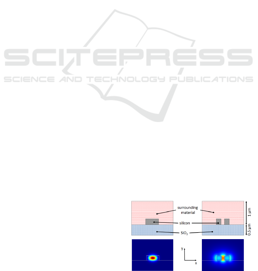
material. Figure 1 shows a detailed cross-sectional
view and compares the guided optical field in a strip-
waveguide to the one of a slot-waveguide. The reason
for this high confinement in-between the silicon rails
is the large-index contrast of the high-index silicon
and the low-index surrounding material. At the inter-
face the normal electric field, which is according to
Figure 1 the E
x
field, undergoes a large discontinuity.
This results in a field enhancement in the low-index
region which is proportional to the ratio of the dielec-
tric constant of the surrounding material to that of sil-
icon.
The high confinement inside the slot is of special
benefit for sensing and electro-optical applications.
The so called silicon-organic hybrid (SOH) technol-
ogy uses organic materials with exceptional high lin-
ear electro-optical coefficients as surrounding mate-
rial (Vivien and Pavesi, 2013). Current electro-optic
modulators are based on semiconductors like silicon.
In silicon photonics, fundamental speed limitations
are related to carrier injection and removal (Vivien
and Pavesi, 2013). Therefore, parametric processes
are impaired by nonparametric processes like two-
photon absorption and become to the main speed lim-
iting factor. Additionally, silicon has a lack of lin-
ear electro-optical coefficients. All this can be over-
come by using organic materials with nonlinear opti-
cal properties as active material.
Slot-waveguides are the key element in order to
integrate organic materials into silicon photonics. Be-
cause the organic materials offer high linear electro-
optical coefficients once can generate advanced mod-
ulation formats (Korn et al., 2013). The reason for
that is that organic materials have less free-carrier
dispersion which normally leads to an intrinsic cou-
pling of amplitude and phase. For that reason, slot-
waveguides have been employed in order to develop
high-speed modulators for telecommunication inter-
connects (Weimann et al., 2014).
In the last decade integrated optical sensors
based on slot-waveguides have also been proposed
(Dell’Olio and Passaro, 2007) and developed (Bar-
Figure 1: Cross-sectional view of a SOI strip-waveguide
(left) and a SOI slot-waveguide (right). The pictures below
show the optical field amplitude distribution. Both waveg-
uide structures are on top of a buried oxide (BOX) substrate.
47
Steglich P., Villringer C., Dümecke S., Padilla Michel Y., Casalboni M. and Schrader S..
Silicon-on-Insulator Slot-waveguide Design Trade-offs.
DOI: 10.5220/0005336200470052
In Proceedings of the 3rd International Conference on Photonics, Optics and Laser Technology (PHOTOPTICS-2015), pages 47-52
ISBN: 978-989-758-093-2
Copyright
c
2015 SCITEPRESS (Science and Technology Publications, Lda.)

rios et al., 2007). In case of label-free bio-sensors it
has been shown that the sensitivity of slot-waveguides
is more than three times higher compared to conven-
tional silicon strip-waveguides (Claes et al., 2009).
This fact is due to the high interaction between guided
light and the surrounding material.
The most challenging issue of SOH technology based
slot-waveguides is the compatibility with common
complementary-metal-oxide-semiconductor (CMOS)
fabrication processes since such integrated photonic
devices need a high integration rate and a cost effi-
cient mass production environment.
For that reason, in this work we present design trade-
offs and an approach in order to improve SOI slot-
waveguide structures for a CMOS-like production en-
vironment. Typical figures of merit like the field con-
finement factor and the effective nonlinear area are
calculated and discussed in detail.
There are several publications about field confinement
factors of slot-waveguide structures. These structures
consist of vertical silicon rails (Robinson et al., 2008)
or multiple nanolayers (Feng et al., 2006). However,
none of them consider SOI slot-waveguides with typ-
ical geometrical dimensions for CMOS-like produc-
tion processes using 200 mm SOI wafers with 220 nm
high SOH slot-waveguides.
In this work we present to our best knowledge a first
comparison of common SOI strip-waveguides with
SOI slot-waveguides by the meaning of modal field
confinement inside the region of interest.
2 SILICON-ON-INSULATOR
SLOT-WAVEGUIDES
A SOI slot-waveguide consist of two silicon rails with
a fixed height of 220 nm due to common CMOS-like
production restrictions. As it can be seen in Figure 1
both silicon rails are located on top of a buried oxide
(BOX) substrate and are separated from each other by
a slot width s and have a rail width w.
Lithographically fabricated slot-waveguides have due
to the side-wall roughness relatively high optical
losses of 10 dB/cm (Baehr-Jones et al., 2005) which
is five times higher compared to common strip-
waveguides (Vivien and Pavesi, 2013). Figure 2
shows one scanning electron microscopy picture of
three slot-waveguides with different slot widths from
the top view and one slot-waveguide in the cross-
sectional view recorded with a focused ion beam.
They are fabricated in a 130 nm SiGe BiCMOS pro-
duction line at the Institute of High-Performance
Microelectronics (IHP) in Frankfurt (Oder) using
200 mm SOI wafers and 248 nm DUV lithography.
Figure 2: Slot-waveguides with different slot widths fabri-
cated with a 248 nm DUV lithography.
Assuming a wavelength of 1550 nm, the refractive in-
dex for the silicon is n
si
= 3.48 and for the BOX sub-
strate n
box
= 1.444 (Palik, 1997; Tsang et al., 2002).
The refractive index of the surrounding material n
sm
is variable because it can be air, gas, fluid or an opti-
cal nonlinear material, depending on the application.
In the following we will use n
clad
as cladding refrac-
tive index instead of n
sm
because we will consider
an organic cladding material. We choose n
clad
= 1.8
which corresponds to a commercially available and
reliable organic material named M3 (commercialized
by GigOptix Inc.). M3 is successfully used for several
slot-waveguide based electro-optical modulators like
in (Palmer et al., 2013a; Leuthold et al., 2013; Korn
et al., 2013; Palmer et al., 2013b).
3 SIMULATION OF
SLOT-WAVEGUIDES
For the calculation of waveguide eigenmodes we em-
ployed a commercial full-vectorial 2D finite element
method (FEM) based mode solver from COMSOL
Multiphysics
r
. Doing this we swept several parame-
ters like the silicon rail width and slot width whereas
the height is fixed to 220 nm and the wavelength is
assumed to be 1550 nm. Triangular vector-elements
with a maximum and minimum element size of 8 nm
and 6 nm, respectively, have been adopted for mesh-
ing the profile. We have always used over 12 · 10
3
mesh elements. For our simulations we consider a
total domain of D
tot
= 3 µm
2
which is illustrated in
Figure 1.
In order to yield the mode field distribution and effec-
tive refractive index, the refractive index distribution
n(x,y) for the structure shown in Figure 1 need to be
declared to calculate eigenvalues and eigenfunctions
of the wave equation
∇ × (∇ × E) − k
2
0
n
2
E = 0, (1)
where k
0
is the wave number in free space. By do-
ing this we get the optical field distribution for the
quasi-TE and quasi-TM mode as shown in Figure 3.
In the following we will neglect the quasi-TM mode
because it is over two times of magnitude smaller than
PHOTOPTICS2015-InternationalConferenceonPhotonics,OpticsandLaserTechnology
48
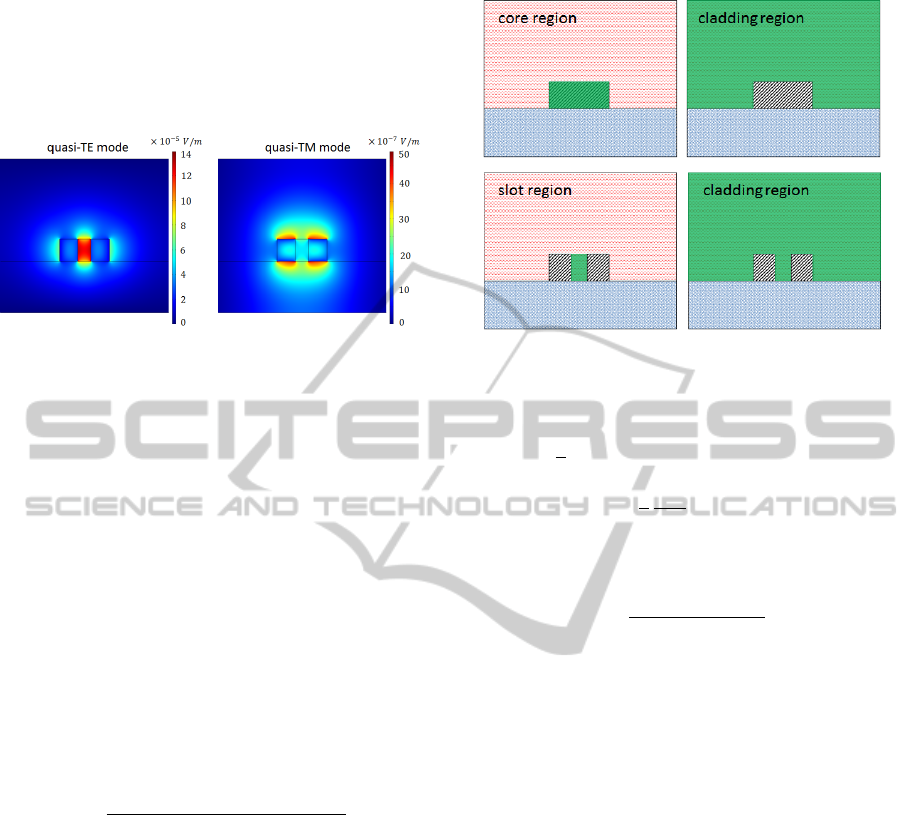
the quasi-TE mode. However, it should be mentioned
that the cross-section capture area for the surface is
typically greater for the quasi-TM mode in biosensing
applications due to the difficulty in functionalising the
interior of the slot.
Figure 3: Optical field distribution for the quasi-TE and
quasi-TM mode of a SOI slot-waveguide.
3.1 Field Confinement Factor of
Slot-waveguides
In order to design, develop and improve slot-
waveguides for applications in the field of biopho-
tonic or high-speed modulators it is necessary to cal-
culate characteristic values which describe the con-
finement and therefore the interaction of light with
the surrounding material. One figure of merit of how
well the guided modal field is confined in a certain
region is the so-called field confinement factor. The
field confinement factor is usually defined as the ra-
tio of the time averaged power flow in the domain of
interest (D
int
) to the time averaged power flow inside
the total domain (D
tot
)
Γ =
Z Z
D
int
Re{[E × H
∗
] · e
z
} dxdy
Z Z
D
tot
Re{[E × H
∗
] · e
z
} dxdy
. (2)
E and H are the electric and magnetic field vectors,
respectively, and e
z
is the unit vector in z direction
(Chuang, 2009). There are three different cases in
order to choose the domain of interest. In case of
common strip-waveguides the domain of interest is
equal to the core region, D
int
=D
core
. In contrast to
that, for bio-sensing applications the region of the
cover medium is considered to be the domain of in-
terest, D
int
=D
cover
, which is valid for strip- and slot-
waveguides as well. Considering slot-waveguides for
electro-optical modulators the domain of interest is
equal to the slot region, D
int
=D
slot
. All possible do-
mains of interest are illustrated in Figure 4. In case
of low-index-contrast waveguides, Equation 2 can be
simplified using the linear relationship between the
electric and magnetic field for a plane-wave
Figure 4: Domains of interest: core D
core
, cladding D
clad
and slot D
slot
regions are highlighted in green. Please note
that the substrate is not included in the cladding region.
1
2
Z Z
Re{[E × H
∗
] · e
z
} dxdy =
1
2
β
ωµ
0
Z Z
|E|
2
dxdy,
(3)
which leads to
Γ =
Z Z
D
int
|E|
2
dxdy
Z Z
D
tot
|E|
2
dxdy
. (4)
However, for high-index-contrast waveguides and
especially for slot-waveguides this linear relation-
ship does not apply since they must satisfy different
boundary conditions (Robinson et al., 2008). Conse-
quently, in this work all confinement factors are cal-
culated according to Equation 2.
3.2 Effective Nonlinear Area of
Slot-waveguides
A figure of merit of how well the waveguide geome-
try supports the nonlinear interaction is the so called
effective nonlinear area (Koos et al., 2007). The
smaller the effective nonlinear area provided by the
waveguide structure the higher the nonlinear interac-
tion which is important for electro-optical modula-
tors.
For the analysis of low-index-contrast systems, it
is usually assumed that the gradient of the dielectric
constant is approximately zero in the entire cross sec-
tion. But this approximation is not valid for high-
index-contrast material systems. Therefore, Koos et
al. derived the effective nonlinear area for high-index-
contrast waveguides in 2007 by using the slowly vary-
ing envelope approximation (Koos et al., 2007). The
Silicon-on-InsulatorSlot-waveguideDesignTrade-offs
49
effective nonlinear area results then from the nonlin-
ear Schr
¨
odinger equation
A
e f f
=
Z
2
0
n
2
clad
·
Z Z
D
tot
Re{[E × H
∗
] · e
z
} dxdy
2
Z Z
D
int
E
4
dxdy
, (5)
with the free-space wave impedance Z
0
=
p
µ
0
/ε
0
≈
377 Ω. In our case is the domain of interest equal
to the cladding domain, D
int
= D
slot
. Equation 5
counts for high-index-contrast material systems. In
case of low-index-contrast material systems it can be
assumed that n
core
≈ n
clad
≈ n
box
≈ n
int
, and the lon-
gitudinal field becomes negligible (Koos et al., 2007).
Furthermore, the transverse components of the elec-
trical field E and the magnetic field H can be ap-
proximated by a scalar function F with the condi-
tion E ≈ F · e
x
and H ≈ (n
int
/Z
0
)F · e
y
where e
x
and
e
y
are the unit vectors in x and y direction, respec-
tively (Koos et al., 2007). Further it can be stated that
D
int
= D
tot
if the nonlinearity is homogeneous in D
tot
.
Now Equation 5 becomes simplified to
A
e f f
=
Z Z
D
tot
F
2
dxdy
2
Z Z
D
int
F
4
dxdy
, (6)
which is similar to the common definition of an effec-
tive area (Agrawal, 2012).
4 RESULTS AND DISCUSSION
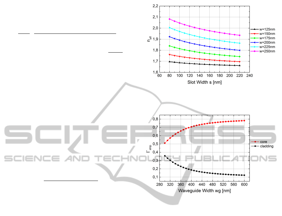
Calculated effective refractive indices n
e f f
as a func-
tion of the slot width s of SOI slot-waveguides are
shown in Figure 5. It can be seen that the effective
refractive index becomes higher by increasing the rail
width w and by decreasing the slot width s.
Figure 6 shows the obtained field confinement fac-
tor Γ
strip
for a silicon strip-waveguide. The domains
of interest are the core and the cladding. Please note
that the substrate is not included in the cladding do-
main. Therefore, the sum of core and cladding field
confinement factor is not equal to unity. As it can be
seen there is a high light confinement in the core re-
gion. These results are in good agreement with the
literature (Vivien and Pavesi, 2013). In order to
maximize the sensitivity of SOI slot-waveguide based
label-free sensors it is necessary to maximize the field
confinement factor of the cladding Γ
clad
. From Figure
7 it can be seen that the confinement in the cladding
region is increased by decreasing the rail width w and
increasing the slot width s. For w = 180 nm the high-
est confinement in the cladding region is obtained in
Figure 5: Calculated effective refractive indices n
e f f
of SOI
slot-waveguides as function of the slot width s and with the
rail width w as parameter.
Figure 6: Field confinement factor Γ
strip
of conventional
SOI strip-waveguides for the core and cladding region as a
function of the waveguide width wg.
the parameter range of our simulation. This result
is in good agreement with (Dell’Olio and Passaro,
2007). For the slot-waveguide with w = 180 nm and
s = 180 nm we obtain a field confinement factor of
Γ
clad
= 0.69. This is an enhancement of about five
times compared to a conventional strip-waveguide
with a typical waveguide width of wg = 500 nm.
With that result, the high sensitivity of slot-waveguide
based label-free sensors as stated by Claes et al. can
be explained (Claes et al., 2009). However, due to the
difficulty in functionalising the interior of the slot the
sensitivity can be smaller than expected.
In order to improve SOI slot-waveguides for
electro-optical applications it is necessary to find the
highest confinement in the slot region. Figure 8 de-
picts the obtained field confinement factors for the slot
region Γ
slot
as a function of the slot width s and the
rail width w as parameter. It can be seen that there
is one maximum of the highest field confinement of
Γ
slot
= 0.216 at a slot width of s = 116 nm and a
rail width of w = 200 nm. This is about four times
smaller compared to a SOI strip-waveguide. How-
ever, in this case it is more convenient to relate the
field confinement factor Γ
slot
to the area where the
PHOTOPTICS2015-InternationalConferenceonPhotonics,OpticsandLaserTechnology
50
Figure 7: Field confinement factor Γ
clad
of a SOI slot-
waveguide for the cladding region in dependence on the slot
width s.
Figure 8: Field confinement factor Γ
slot
of a SOI slot-
waveguide for the slot region as a function of the slot width
s and the rail width w as parameter.
Figure 9: Calculated effective nonlinear area A
e f f
of SOI
slot-waveguides in dependence on the slot width s. The rail
width w was varied as parameter.
light is confined as figure of merit, FOM = Γ
slot
/A
slot
and FOM = Γ
strip
/A
strip
. In our case A
slot
is equal
to D
slot
and A
strip
is equal to D
core
. With that we
can show for our example that the FOM for a SOI
slot-waveguide (s = 116 nm, w = 200 nm) is about
four times higher compared to that one of a strip-
waveguide (wg = 500 nm) which confirms our results
for the cladding field confinement and other publica-
tions like (Almeida et al., 2004).
Furthermore, it is necessary to minimize the effec-
tive nonlinear area A
e f f
in order to improve SOI slot-
waveguides for third order nonlinear effects. Figure
9 indicates that there is a minimum in the parameter
range of our simulation of A
e f f
= 0.032 µm
2
for a slot
width of s = 80 nm and a rail width of w = 225 nm.
Our results are in good agreement with (Muellner
et al., 2009).
5 CONCLUSION
Simulation and analysis of SOI slot-waveguides have
been carried out and field confinement factors and
effective nonlinear areas have been thoroughly cal-
culated with the Finite Element Method. Field con-
finement factors have been calculated in the slot and
cladding region. According to our simulation, SOI
slot-waveguides provide about five times higher field
confinement in the cladding region compared to con-
ventional SOI strip-waveguides. These results can be
used for design optimization in order to achieve op-
timal SOI slot-waveguide dimensions for sensing ap-
plications. For the slot region we have found a maxi-
mum confinement of Γ
slot
= 0.216 which is compared
to a SOI strip-waveguide about four times smaller.
However, relating it to the area there the light is con-
fined it is four times higher compared to a SOI strip-
waveguide. For the effective nonlinear area we have
found a minimum of about A
e f f
= 0.032 µm
2
for our
simulated parameter range. In total, we have demon-
strated design trade-offs and an approach in order to
improve SOI slot-waveguide structures.
ACKNOWLEDGEMENTS
The authors would like to thank the German Federal
Ministry of Education and Research (BMBF) for the
financial support under contract no. 03FH086PX2,
the University of Applied Sciences Wildau (THWi),
Germany, and the Ministry of Science, Technology
and Culture of the federal state Brandenburg, Ger-
many, for financial support. The authors would also
like to thank Fr. Nanni, P. Prosposito, F. De Matteis,
and R. De Angelis from the University of Rome Tor
Vergata, Italy, St. Meister and A. Al-Saadi from the
Technical University Berlin, Germany, and L. Zim-
mermann, D. Knoll, D. Stolarek, J. Katzer, St. Lis-
chke, H. Silz, B. Tillack and W. Mehr from the In-
stitute of High-Performance Microelectronics (IHP),
Germany, for their encouragement and support in the
framework of the Joint-Lab IHP-THWi.
Silicon-on-InsulatorSlot-waveguideDesignTrade-offs
51

REFERENCES
Agrawal, G. (2012). Nonlinear Fiber Optics. Academic
Press, 5 edition.
Almeida, V. R., Xu, Q., Barrios, C. A., and Lipson, M.
(2004). Guiding and confining light in void nanos-
tructure. Opt. Lett., 29(11):1209–1211.
Baehr-Jones, T., Hochberg, M., Walker, C., and Scherer,
A. (2005). High-q optical resonators in silicon-on-
insulator-based slot waveguides. Applied Physics Let-
ters, 86(8):081101.
Barrios, C. A., Gylfason, K. B., S
´
anchez, B., Griol,
A., Sohlstr
¨
om, H., Holgado, M., and Casquel, R.
(2007). Slot-waveguide biochemical sensor. Opt.
Lett., 32(21):3080–3082.
Chuang, S. L. (2009). Physics of Photonic Devices. Wiley,
2 edition.
Claes, T., Molera, J., De Vos, K., Schachtb, E., Baets, R.,
and Bienstman, P. (2009). Label-free biosensing with
a slot-waveguide-based ring resonator in silicon on in-
sulator. Photonics Journal, IEEE, 1(3):197–204.
Dell’Olio, F. and Passaro, V. M. (2007). Optical sensing
by optimized silicon slot waveguides. Opt. Express,
15(8):4977–4993.
Feng, N.-N., Michel, J., and Kimerling, L. (2006). Optical
field concentration in low-index waveguides. Quan-
tum Electronics, IEEE Journal of, 42(9):885–890.
Koos, C., Jacome, L., Poulton, C., Leuthold, J., and Freude,
W. (2007). Nonlinear silicon-on-insulator waveg-
uides for all-optical signal processing. Opt. Express,
15(10):5976–5990.
Korn, D., Palmer, R., Yu, H., Schindler, P. C., Alloatti,
L., Baier, M., Schmogrow, R., Bogaerts, W., Sel-
varaja, S. K., Lepage, G., Pantouvaki, M., Wouters,
J. M., Verheyen, P., Campenhout, J. V., Chen, B.,
Baets, R., Absil, P., Dinu, R., Koos, C., Freude,
W., and Leuthold, J. (2013). Silicon-organic hybrid
(soh) iq modulator using the linear electro-optic effect
for transmitting 16qam at 112 gbit/s. Opt. Express,
21(11):13219–13227.
Leuthold, J., Koos, C., Freude, W., Alloatti, L., Palmer, R.,
Korn, D., Pfeifle, J., Lauermann, M., Dinu, R., Wehrli,
S., et al. (2013). Silicon-organic hybrid electro-optical
devices. Selected Topics in Quantum Electronics,
IEEE Journal of, 19(6):3401413–3401413.
Muellner, P., Wellenzohn, M., and Hainberger, R.
(2009). Nonlinearity of optimized silicon photonic
slot waveguides. Opt. Express, 17(11):9282–9287.
Palik, E. D. (1997). Handbook of Optical Constants of
Solids. Academic Press, 1 edition.
Palmer, R., Alloatti, L., Korn, D., Schindler, P., Baier,
M., Bolten, J., Wahlbrink, T., Waldow, M., Dinu, R.,
Freude, W., Koos, C., and Leuthold, J. (2013a). Low
power mach-zehnder modulator in silicon-organic hy-
brid technology. Photonics Technology Letters, IEEE,
25(13):1226–1229.
Palmer, R., Alloatti, L., Korn, D., Schindler, P., Schmogrow,
R., Heni, W., Koenig, S., Bolten, J., Wahlbrink, T.,
Waldow, M., Yu, H., Bogaerts, W., Verheyen, P., Lep-
age, G., Pantouvaki, M., Van Campenhout, J., Absil,
P., Dinu, R., Freude, W., Koos, C., and Leuthold, J.
(2013b). Silicon-organic hybrid mzi modulator gener-
ating ook, bpsk and 8-ask signals for up to 84 gbit/s.
Photonics Journal, IEEE, 5(2):6600907–6600907.
Robinson, J. T., Preston, K., Painter, O., and Lip-
son, M. (2008). First-principle derivation of gain
in high-index-contrast waveguides. Opt. Express,
16(21):16659–16669.
Tsang, H., Wong, C., Liang, T., Day, I., Roberts, S., Harpin,
A., Drake, J., and Asghari, M. (2002). Optical dis-
persion, two-photon absorption and self-phase mod-
ulation in silicon waveguides at 1.5 µm wavelength.
Applied Physics Letters, 80(3):416–418.
Vivien, L. and Pavesi, L., editors (2013). Handbook of Sili-
con Photonics. CRC Press, 0 edition.
Weimann, C., Schindler, P. C., Palmer, R., Wolf, S., Bekele,
D., Korn, D., Pfeifle, J., Koeber, S., Schmogrow, R.,
Alloatti, L., Elder, D., Yu, H., Bogaerts, W., Dal-
ton, L. R., Freude, W., Leuthold, J., and Koos, C.
(2014). Silicon-organic hybrid (soh) frequency comb
sources for terabit/s data transmission. Opt. Express,
22(3):3629–3637.
PHOTOPTICS2015-InternationalConferenceonPhotonics,OpticsandLaserTechnology
52
