
Fabrication of Surface Relief Optical Elements in Ternary
Chalcogenide Thin Films by Direct Laser Writing
I. Voynarovych
1
, R. Poehlmann
2
, S. Schroeter
2
and M. Vlcek
1
1
Department of General and Inorganic Chemistry, Faculty of Chemical Technology, University of Pardubice,
Studentska 573, Pardubice, Czech Republic
2
Leibniz Institute of Photonic Technology, Albert-Einstein-Str. 9, Jena, Germany
Keywords: Direct Laser Writing, Chalcogenide Glasses, Patterned Structures.
Abstract: Direct laser writing with a continuous-wave high intensity and over-band gap laser is applied to realize
surface relief optical elements in ternary As-S-Se and Ge-As-S thin chalcogenide films. The topology of
created structures in dependence on the experimental conditions is investigated. Analyses indicate that the
formation mechanisms of the surface patterns are thermally induced processes generated by the local
heating and involve thermoplastic deformation, mass flow induced by the surface tension gradient and
evaporation. Diffractive gratings with a period of 2.56 m, depths of up to 100 nm, and different periodic
surface structures were patterned at the surface of 1 m thick films. The spectral dependencies of diffraction
efficiency were measured and discussed.
1 INTRODUCTION
The chalcogenide glass (ChG) family exhibits
several interesting properties that can be exploited
e.g. in optical communication, optical sensing, high
density optical recording, and optical lithography. In
particular, their excellent infrared transparency up to
12–20 m, large third order susceptibility, high
refractive index (usually 2–3.2), and ability to
undergo significant irradiation induced structural
modifications make chalcogenide glass films good
candidates for the fabrication of all-optical switches
(Harbold, 2002) and integrated optical elements
(Meneghini, 1998; Viens, 1999). Optical integrated
as well as diffractive elements in chalcogenide
glasses have been fabricated by several techniques
including interference photolithography (Utsugi,
1975; Chomat, 1976; Palyok, 1999), ion
implantation and direct ion/laser beam writing
(Schroeter, 2007; Nordman, 1996). The direct laser
writing (DLW) by a tightly focused laser beam has
been intensively developed during the last decades
as an efficient way to produce 2D and 3D
microstructures. It attracts high interest due to its
inherent advantages like high precision, moderate
cost, high speed, and high flexibility (Thiel, 2010;
Van, 2009).
Among all the variety of chalcogenide glasses
(ChGs), i.e. glasses containing chalcogen elements
(e.g. S, Se, Te), arsenic trisulfide As
2
S
3
(As
40
S
60
) is
one of the most studied and well-known. A
particular interest attract ternary compositions based
on As
2
S
3
for which the substitution of S by Se gives
the possibility to monotonically change optical
properties such as the band gap energy, from 2.4 eV
down to 1.8 eV, and the refraction coefficient from
2.3 up to 2.7 (Gonzalez-Leal, 2003), whereas the
substitution of tri-coordinated As by four-
coordinated Ge causes the glass network to change
from a two-dimensional layered structure to a three-
dimensional structure with a more rigid network
resulting in a significant change of the
thermodynamic properties such as softening
temperatures, viscosity etc. (Feltz, 1993;
Tatsumisago, 1990).
In this paper we compare the behavior of
different ternary As-S-Se as well as Ge-As-S thin
films under cw laser exposure in dependence on the
writing conditions and demonstrate the possibility to
fabricate surface relief diffractive optical elements
by DLW.
2 EXPERIMENTAL
Bulk samples of As and Ge based glasses from
134
Voynarovych I., Poehlmann R., Schroeter S. and Vlcek M..
Fabrication of Surface Relief Optical Elements in Ternary Chalcogenide Thin Films by Direct Laser Writing.
DOI: 10.5220/0005404001340139
In Proceedings of the 3rd International Conference on Photonics, Optics and Laser Technology (PHOTOPTICS-2015), pages 134-139
ISBN: 978-989-758-093-2
Copyright
c
2015 SCITEPRESS (Science and Technology Publications, Lda.)

ternary systems As-S-Se and Ge–As–S were prepared
by conventional melt-quenching method from high
purity (5 N) elements in evacuated quartz ampoules
for 8 h at 650
o
C (As based samples) or 1000
o
C (Ge
based samples) in a rocking furnace. Thin-film
samples were prepared by vacuum evaporation of
the bulk glassy materials onto clean glass substrates.
The thermal evaporation process was performed
within a coating system (Tesla Corporation, model
UP-858) at a pressure of about 10
-3
Pa. During the
deposition process the substrates were conveniently
rotated by means of a planetary rotation system to
ensure high homogeneity of the film thickness. The
deposition rate was in the range 1–2 nm/s, measured
continuously using the quartz microbalance technique.
The thickness of the thin films was about 1 m
The laser lithography system DWL 66,
Heidelberg Instruments Mikrotechnik GmbH,
equipped with a vertically polarized continuous-
wave He-Cd laser (=442 nm) was used for the
exposures. The maximal laser power available after
the writing objective to expose the samples was
P
max
=1.8 mW. The laser beam was focused to a spot
diameter of about 640 nm by an objective with a
focal length of 4 mm and a numerical aperture of
0.85. The focus distance of the objective is
controlled by an air gauge based autofocus system.
The applied exposure laser power P was tuned by a
rotable polarizer in steps of 10% from P
max
down to
0.4P
max
, resulting in spot intensities between
5.610
5
W/cm
2
and 2.210
5
W/cm
2
. Structures were
patterned at writing speeds of 25-75 mm/s. An
atomic force microscope (Ultraobjective SIS
attached to an optical microscope) was used to
investigate the morphology of the corrugated surface
of the thin films. The transmission spectra and
diffraction efficiencies were measured with the fiber
coupled spectrometer EPP2000 (StellarNet Inc.)
3 RESULTS AND DISCUSSION
To compare the behavior of thin chalcogenide films
with different optical and thermodynamic properties
under the irradiation with an over band-gap cw laser
a series of single lines was written with different
laser intensities ranging from 2.210
5
to
5.610
5
W/cm
2
on each of the samples of the
different investigated compositions. Created surface
structures were investigated by atomic force
microscopy, and the geometrical profiles of each
line were taken by scanning in the direction
perpendicular to the laser beam movement. The
analysis of such profiles shows that they can be
divided into three main groups (see inset of Fig.1)
indicating various possible formation mechanisms
depending on the laser intensity as well as on the
properties of the distinct thin film.
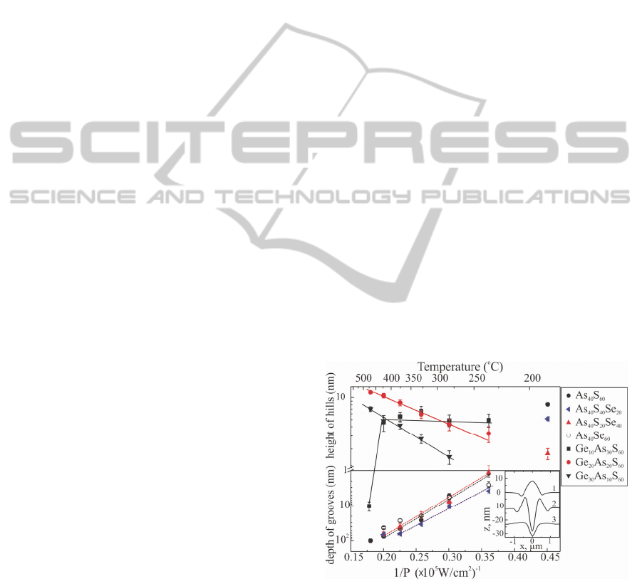
The curve 1 in the inset of Fig.1 represents a
typical profile for photo-induced expansion that
appears at all used intensities for Ge-As-S thin films
and at low intensity of the writing laser beam for As-
S-Se compositions. In this case the shape of the
corrugated structure follows the Gaussian intensity
profile of the laser beam. The dependences of the
height of the emergent elevations (‘hills’) on the
laser intensity are shown in the upper part of Fig. 1
for different compositions.
The curve 2 in the inset of Fig.1 represents
emerging profiles for the case that a groove with a
simultaneously appearing rim surrounding the center
of the laser spot is created. Formation of such a
profile is typical only for As-S-Se thin films above
an experimentally determined threshold value of
2.810
5
W/cm
2
, whereas for Ge-based ternary
compositions only the creation of grooves without
any rim (see curve 3) was observed. The magnitude
of the groove depth obtained from the AFM images,
is represented in the lower part of Fig. 1 as a
function of exposure intensity for the different
compositions.
As we used an over-bandgap writing laser the
beam energy was totally absorbed within a small
volume of the thin film. The penetration depth d
pd
of
the He-Cd laser beam was evaluated according to
the Beer-Lambert law as d
pd
=1/
(
absorption
coefficient). For As
40
S
60-x
Se
x
compositions d
pd
varies
from 240 nm (x=0) down to 80 nm (x=60) and for
the Ge-based compositions d
pd
is 240 nm almost
independent on the composition. Because of the
extremely high intensity and the total absorption of
the light within a very small volume, the thin
chalcogenide film can be locally and rapidly heated
up to temperatures above T
g
, or even to temperatures
where material decomposition and evaporation take
place. The temperatures on the surface at the center
of a stationary Gaussian heat source for a semi-
infinite solid can be calculated as (Carslaw, 1959):
/
2
√
∗
,
(1)
where, t – duration of laser interaction with the thin
film, w – waist of the laser beam (0.64 m), K and D
are the thermal conductivity and diffusivity of the
glass substrate (110
-2
W/K*cm and 5.3310
-3
cm
2
/s
respectively), P
a
=P(1-R), where P is the power of
the incident beam and R the reflectivity at the air-
film interface. The potential of this model to
FabricationofSurfaceReliefOpticalElementsinTernaryChalcogenideThinFilmsbyDirectLaserWriting
135
describe the thermal evolution in chalcogenide thin
films during over-band gap cw laser irradiation was
demonstrated (Nordman, 1999). The temperatures
calculated for our experimental conditions are
shown as the top axis on Fig.1.
The most common and simple, but remarkably
accurate, relation between the changing rate of any
kinetic parameter and the temperature change is
given by the Arrhenius equation: F=A·exp(-E
a
/k
B
T),
where F is a rate constant, A the pre-exponential
factor, E
a
the activation energy for the change to
take place, T the temperature, and k
B
the Boltzmann
constant.
As can be seen from Eq. (1), the temperature on
the thin film surface is proportional to the laser beam
intensity. The straight line dependences for the depth
of grooves for As-based thin films as well as of the
height of hills for Ge-based compositions (see Fig.1)
on the inverse of the beam intensity (and thus on the
inverse temperature) clearly show that both
parameters obey Arrhenius' equation and we can
thus conclude that the formation mechanisms of the
patterned structures are thermally-induced processes.
The temperature of the thin film’s surface for
exposure power levels at which solely expansion
was observed is close to the glass softening
temperature (180-210
o
C range for As-S-Se and 230-
440
o
C for Ge-As-S ternary compositions (Feltz,
1993). The most realistic mechanism is in this case
the thermoplastic deformation proposed in Refs.
(Zhao, 2013; Shiu, 1999). According to this
mechanism, a locally heated volume expands
preferably in the direction to the film’s interface
with air because of the suppresion of expansion in
other directions by the unheated glass and the plastic
deformation due to the yield stress of heated and
thus softened material.
When, however, the surface temperature of the
chalcogenide film at still higher laser intensities
exceeds the softening temperature of a given glass
composition the viscosity of the exposed material
begins to decrease (Feltz, 1993) and thus melts in
the irradiated spot area resulting in a different
surface corrugation mechanism. The processes of
surface corrugation for the case of a locally molten
material area were theoretically and experimentally
investigated by several authors (Blom, 1983; Cline,
1981; Anthony, 1977). According to the proposed
model, the molten material is pulled from the center
of the molten spot by a shear stress and forms the
rim surrounding the central hole (curve 2 in the inset
of Fig.1), which is the result of a surface tension and
a viscosity gradient, in turn resulting from a
temperature gradient induced by the focused laser
beam with a Gaussian intensity profile. In the case
of Ge-based ternary compositions, the more rigid
glass structure and thus the smaller temperature
dependence of the viscosity (Tatsumisago, 1990) in
combination with a counterflow induced by capillary
pressure can prevent the viscous flow in the given
temperature region.
At the highest intensities available for exposures
only for As-based compositions the process of
decomposition/evaporation−back-condensation takes
place when the temperature exceeds the
experimentally determined threshold temperature of
about 370
o
C.
Having in detail investigated the power
dependence of the resulting structural parameters we
have chosen the maximal available intensity of
5.6x10
5
W/cm
2
and a scan speed of 75 mm/s to
pattern surface relief gratings with a period of
=2.54 m and an area of 5x5 mm
2
into ternary As-
S-Se and Ge-As-S thin films. In Fig.2 are shown the
AFM images of diffraction gratings with a period
=2.54 m patterned by DLW with the chosen
writing parameters on the surface of As
2
S
3
(a) and
Ge
25
As
15
S
60
(b) thin films. The groove depth for the
Ge-containing thin films was only up to 12 nm and
the gratings exhibit thus only very low diffraction
efficiency. But these gratings can be further
developed by wet or dry etching. However, the
depth of grooves for a diffraction grating on As-S-Se
thin films can vary from a few nanometers up to
about 100 nm by choosing appropriate writing
parameters.
Figure 1: Dependences of depth of grooves and height of
hills of corrugated structures on the exposed intensity
(bottom axis) and calculated surface temperature (top axis)
for different ternary Ge-based and As-based thin films.
For the used writing parameters given above the
quality of the grating surface for the As
2
S
3
film is
very good, whereas for lower writing speeds
evaporation and back-condensation processes start to
PHOTOPTICS2015-InternationalConferenceonPhotonics,OpticsandLaserTechnology
136
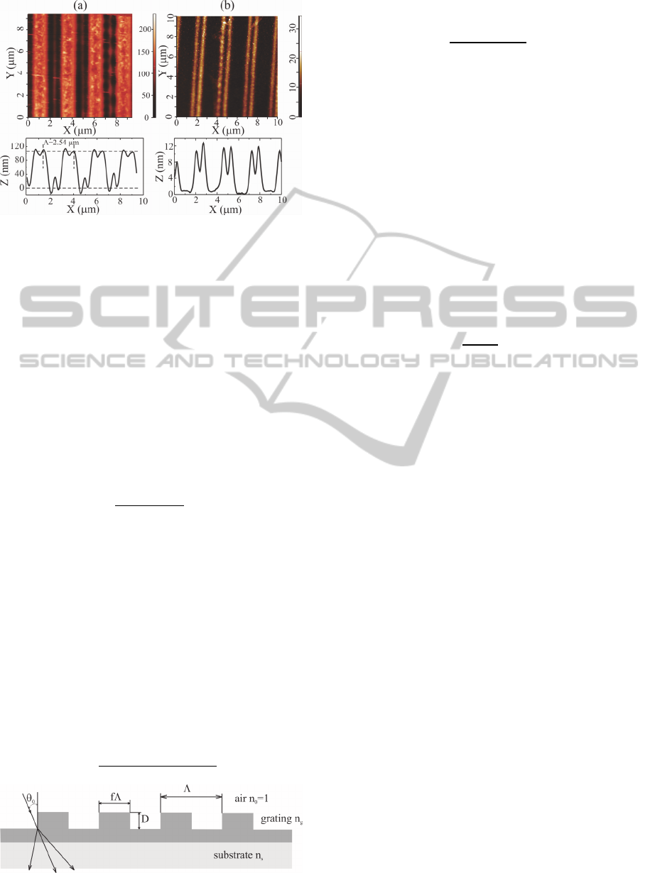
Figure 2: AFM scan and averaged profile of the surface
relief grating formed by DLW on the surface of As
2
S
3
(a)
and Ge
25
As
15
S
60
(b) thin films written with an intensity of
5.610
5
W/cm
2
and a scan speed 75 mm/sec.
take place and randomly spread small material
particles emerge at the surface. This causes an
increased level of stray light deteriorating the
diffraction properties.
Binary surface relief diffractive elements can
exhibit very high diffraction efficiency. Let us
consider the case of a surface relief phase grating on
a thin film evaporated on a usual glass substrate as
shown in Fig. 3.
To define whether a grating is thin or thick the
parameter Q can be used (Collier, 1971):
2
Λ
cos
(2)
where
is the free space wavelength, D the grating
thickness, n the average refractive index. For our
structural parameters Q is less than 1 defining the
grating as thin. Applying the scalar diffraction
theory and neglecting the reflection at the air-film
interface for a thin binary surface relief grating with
a fill
factor f, the zero-order transmittance efficiency
into the grating material can be derived as (Jing,
2011)
12
1
∙1Δ,
(3)
whereas for the other diffraction orders m the
efficiency
is given by:
,
(4)
Figure 3: Binary diffraction grating.
with
Δ
2
1
(5)
As can be seen from Eq. 4, the maximal diffraction
efficiency into the first order is
4/
0.405
for the case f=0.5 and
=.
Approximating the grating profile shown in Fig.
2(a) by a binary structure with D=90 nm, and using
the index of refraction for As
2
S
3
(Laniel, 2003)
decreases from 0.96 at
=400 nm to 0.295 at
=1000 nm.
Taking also into account the Fresnel reflection R
at the interface of the chalcogenide film with the air
for the case of normal incidence (
0
=0) the
efficiencies calculated from Eqs. (3) and (4) are
reduced by the factor 1-R, with
1
1
(6)
The diffraction efficiencies into the chalcogenide
film according to the scalar diffraction theory as
calculated using Eq. (3) to Eq. (6) are represented in
Fig. 4.
For comparison are also shown the results of a
rigorous calculation applying the Rigorous Coupled
Wave Analysis (RCWA) (Moharam, 1982).
The main reason for the differences between the
simulations and the measured diffraction efficiencies
is that the calculations are made for the diffraction
into the chalcogenide film and do not take into
account that the diffracted powers in the experiment
are measured after propagation through the
unstructured part of the layer and the glass substrate
into air. For the short wavelength range the
absorption of As
2
S
3
(Laniel, 2003) reduces the
transmitted power significantly. With increasing
wavelength the absorption of As
2
S
3
is rapidly
decreasing, however the reflections at the interfaces
chalcogenide glass / glass substrate and substrate/air
can lower the transmission. Accordingly the
experimental results are spectrally modulated in
similarity with the transmission of the unstructured
thin film also shown in Fig. 4.
In the focus of interest are currently also
photonic crystals composed of periodic
microstructures that affect the propagation of
electromagnetic and/or plasmonic waves in a
specific manner and offer unique properties for the
realization of different photonic devices. Examples
of such periodic surface microstructures that were
FabricationofSurfaceReliefOpticalElementsinTernaryChalcogenideThinFilmsbyDirectLaserWriting
137
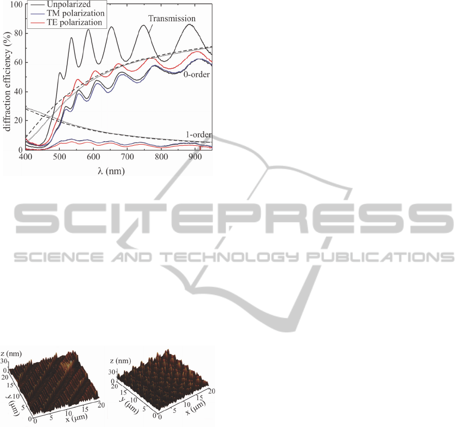
Figure 4: Spectral dependence of thin film transmission, 0-
order and 1-order diffraction efficiencies (solid lines)
measured for normal incidence at a grating prepared by
DLW on the surface of an As
2
S
3
thin film with an intensity
of 5.610
5
W/cm
2
and a scan speed of 75 mm/sec and
diffraction efficiencies calculated with scalar and rigorous
diffraction theories (dashed and dotted line respectively).
fabricated by DLW with a resolution down to about
1 m in a Ge
20
As
20
S
60
chalcogenide thin film are
shown in Fig. 5. However, for practical applications
a post-exposure etching process would be required
in order to significantly increase the depth of the
structures.
Figure 5: AFM images of periodic arrays with different
pattern shapes created by DLW in a Ge
20
As
20
S
60
thin film.
4 CONCLUSIONS
The surface corrugation processes induced by the
irradiation of ternary As
40
S
60-x
Se
x
and Ge
x
As
40-x
S
60
thin films with a continuous wave tightly focused
overband-gap laser emitting at 442 nm were
investigated.
Analyses of the topology of the created
structures indicate that the formation mechanisms of
the surface patterns are thermally induced processes
generated by the local heating and involve
thermoplastic deformation, mass flow induced by
surface tension gradient and decomposition/
evaporation mechanism.
By tuning the laser power diffractive optical
elements like diffraction gratings with a period of
2.56 m and various depths or periodic surface
microstructures with feature sizes down to less than
1 micrometer and different shapes were patterned.
The zero- and first-order diffraction efficiencies
were measured for a diffractive grating in a As
2
S
3
thin film within the visible and near infrared spectral
range. A maximal value of 8% for the first
diffraction order was measured.
ACKNOWLEDGEMENTS
This work was supported by the grant
CZ.1.07/2.3.00/30.0058 from the Czech Ministry of
Education, Youth and Sports
REFERENCES
Anthony T. R. and Cline H. E., 1977 ‘Surface rippling
induced by surface tension gradients during laser
surface melting and alloying’, J. Appl. Phys., vol. 48,
pp.3888-3894.
Blom G. M., 1983 ‘Hole formation in tellurium alloy films
during optical recording’, J. Appl. Phys., vol.54,
pp.6175-6182.
Carslaw H. S. and Jaeger J. C., 1959. Conduction of Heat
in Solids, Oxford University, Oxford, 2
nd
ed.
Chomat H., Lezal D., Gregora I., and Srb I., 1976 ‘Relief
holograms in thin films of amorphous As
2
Se
3
under
high laser exposures’, J. Non-Cryst. Solids, vol.20,
pp.427-437.
Cline E., 1981 ‘Surface rippling induced in thin films by a
scanning laser’, J. Appl. Phys., vol.52, pp.443-448.
Collier R. J., Burckhardt C. B., Lin L. H. 1971. Optical
holography, Academic Press, - Technology &
Engineering, 605 p.
Feltz A. 1993 ‘Amorphous Inorganic Materials and
Glasses’, VCH Weinheim/VCH Publishers, New
York,. 446 p.
Gonzalez-Leal J.M., Prieto-Alcon R., Angel J.A., Marquez
E., 2003 ‘Optical properties of thermally evaporated
amorphous As
40
S
60-x
Se
x
films’, Journal of Non-
Crystalline Solids, vol. 315 pp.134–143.
Harbold J. M., Ilday F. O., Wise F. W., Sanghera J. S.,
Nguyen V. Q., Shaw L. B., Aggarwal I. D., 2002
‘Highly nonlinear As-S-Se glasses for all-optical
switching’, Opt. Lett.,vol. 27, pp.119-121.
Jing X., Jin Y., 2011 ‘Transmittance analysis of diffraction
phase grating’, Applied Optics, vol.50. pp. c11-c18.
Laniel J. M., Menard J., Turcotte K., Villeneuve A.,
Vallee R., Lopez C., Richardson K. A., 2003
‘Refractive index measurements of planar
chalcogenide thin film’, J. Non-Cryst. Solids, vol. 328,
PHOTOPTICS2015-InternationalConferenceonPhotonics,OpticsandLaserTechnology
138

pp. 183–191.
Meneghini C., Villeneuve A., 1998 ‘As
2
S
3
photosensitivity
by two-photon absorption: holographic gratings and
self-written channel waveguides’, J. Opt. Soc. Am. B
vol. 15, pp. 2946-2950.
Moharam M. G., and Gaylord T. K., 1982 ‘Diffraction
analysis of dielectric surface-relief gratings’, J. Opt.
Soc. Am. vol.72, pp.1385-1392.
Nordman N., Salminen O., Kuittinen M., and Turunen
J.,1996 ‘Diffractive phase elements by electron-beam
exposure of thin As
2
S
3
Films’, J. Appl. Phys., vol. 80,
pp.1079-1080.
Nordman O. and Nordman N., 1999 ‘Hole formation
induced by 488.0-nm light in 10-mm-thick amorphous
as-evaporated As
2
S
3
films’, Phys. Rev. B: Condens.
Matter., vol. 60, pp.2833-2838.
Palyok V., Mishak A., Szabo I., Beke D. L., Kikineshi A.,
1999 ‘Photoinduced transformations and holographic
recording in nanolayered a-Se/As
2
S
3
and AsSe/As
2
S
3
films’, Appl. Phys. A, vol. 68, pp. 489-492.
Schroeter S., Vlcek M., Poehlmann R., Fiserova A., 2007
‘Efficient diffractive optical elements in chalcogenide
glass layers fabricated by direct DUV laser writing’, J.
Phys. Chem. Solids, vol. 68, pp.916–919.
Shiu T., Grigoropoulos C. P., Cahill D. G., and Greif R.,
1999 ‘Mechanism of bump formation on glass
substrates during laser texturing’, J. Appl. Phys., vol.
86, pp.1311-1316.
Tatsumisago M., Halfpap B. L., Green J. L., Lindsay S.
M., and Angell C. A., 1990 ‘Fragility of Ge-As-Se
glass-forming liquids in relation to rigidity
percolation, and the Kauzmann paradox’, Phys. Rev.
letters, vol. 64, pp.1549-1552.
Thiel M., Fischer J., von Freymann G., Wegener M., 2010,
‘Direct laser writing of three-dimensional submicron
structures using a continous-wave laser at 532nm’,
Appl. Phys. Lett. vol. 97, p.221102.
Utsugi Y. & Zembutsu S., 1975 ‘Relief type diffraction
grating by amorphous chalcogenide films’, Appl. Phys.
Lett. vol. 27, pp.508-510.
Van Gough D., Juhl A. T. and Braun P. V. 2009,
‘Programming structure into 3D nanomaterials’,
Materials today, vol. 12, p.28.
Viens J-F., Meneghini C., Villeneuve A., Galstian T. V.,
Knystaunas E. J., Duguay M. A., Richardson K. A.,
Cardinal T., 1999 ‘Fabrication and characterization of
integrated optical waveguides in sulfide chalcogenide
glasses’, J. Lightwave Technology vol. 17, pp.1184-
1191.
Zhao D., Jain H., Malacarne L. C., and Pedreira P. R. B.,
2013 ‘Role of photothermal effect in photoexpansion
of chalcogenide glasses’, Phys. Status Solidi B, vol.
250, pp.983–987.
FabricationofSurfaceReliefOpticalElementsinTernaryChalcogenideThinFilmsbyDirectLaserWriting
139
