
Analysis and Design of Hybrid and Graphene-Based
Plasmonic Waveguide Components
D. A. Ketzaki, V. Salonikios, I. Demirtzioglou and T. V. Yioultsis
Dept. of Electrical and Computer Engineering, Aristotle University of Thessaloniki, Thessaloniki, Greece
traianos@auth.gr
Keywords: Graphene, plasmonics, plasmonic waveguides, hybrid waveguides.
Abstract: We present an efficient finite element formulation for the eigenmode analysis of graphene-based plasmonic
waveguides with switching functionalities. The formulation is full-vectorial and addresses graphene as a
surface conductivity, as opposed to bulky material considerations, thus eliminating the need for fine
discretizations inside thin graphene models. Based on this technique, several graphene-enhanced plasmonic
waveguides and components with promising characteristics are proposed.
1 INTRODUCTION
Graphene is a relatively new innovative material,
with interesting new physics and several significant
properties and effects, including the ability to
support surface plasmon propagating modes and
switching functionalities (Bludov et al., 2013).
Optical conductivity of graphene has been shown to
consist of a Drude intraband term and an interband
contribution. These properties may result in either
plasmonic modes in THz (Nikitin et al., 2011) or
enhanced switching in photonic waveguides for the
optical communications regime (Sun et al., 2014). In
particular, for the case of the THz regime, where the
Drude term is dominant, graphene surface plasmons
offer the possibility of waveguiding with strong
confinement, while in the optical communications
spectrum where the interband contribution is
substantial, the tunability of graphene’s conductivity
through electrostatic gating shows great potential for
the design of switching components.
As for the analysis and design of graphene-based
and enhanced waveguides and components, the
finite element method (FEM) is a perfect candidate,
due to its ability to deal with problems of
considerable geometric complexity. However, the
general trend is often to approach graphene as a
bulky material, thus requiring very fine
descritizations inside thin sheets and the surrounding
space as well. We present here an efficient
formulation for both the eigenmode and the 3D
analysis of graphene-based plasmonic waveguides
and components with switching functionalities
which is full-vectorial and addresses graphene as a
thin sheet with a surface conductivity. Based on this
analysis, we propose a graphene-enhanced
plasmonic CGS waveguide with an extinction ratio
of 8.6 dB and a 2.15 dB insertion loss for a 10 um
length, which can be considered highly satisfactory.
A particular investigation of a three-dimensional
microring /microdisk filter revelas the possibility of
actual designs with extinction ratios exceeding 10
dB, which is also a firm basis for further study
towards the development of switched plasmonic
components in the photonics regime.
2 FINITE ELEMENT
FORMULATION
The proposed finite element eigenmode formulation
follows the general framework that has been
proposed in (Selleri et al., 2001), where the electric
field is used as a working variable. The formulation
uses mixed finite elements for the discretization of
the waveguide cross section, with tangentially
continuous (H-curl) vector finite elements in the
transverse plane and scalar (nodal) finite elements
for the axial component. Using the Galerkin
formulation for the Helmholtz equation, the form
12
0
0
rr
S
k dsEEΕ
(1)
expresses the projected problem, reducing its
solution to a finite-dimensional vector subspace. The
24
Ketzaki D., Salonikios V., Demirtzioglou I. and Yioultsis T.
Analysis and Design of Hybrid and Graphene-Based Plasmonic Waveguide Components.
DOI: 10.5220/0005888900240028
In Proceedings of the Fourth International Conference on Telecommunications and Remote Sensing (ICTRS 2015), pages 24-28
ISBN: 978-989-758-152-6
Copyright
c
2015 by SCITEPRESS – Science and Technology Publications, Lda. All rights reserved

electric field can be written in the form
z
tz
EeE E z
, where
( , )
tt
xyEE
represents
the transverse component and
( , )
zz
E E x y
represents the axial component. The adjoint field
z
tz
EeE E z
is selected as the test function in
the Galerkin equation and the final eigenmode
formulation expressed as a function of the effective
refractive index
0
/
eff
n j k
is as follows:
1
,
1
,
22
0 , 0 ,
1
0,
1
0,
2 2 1
0,
t r zz t
S
z r tt z
S
t r tt t z r zz z
SS
t r tt z
S
eff
z r tt t
S
eff t r tt t
S
ds
E E ds
k ds k E E ds
jk E ds
n
jk E ds
n k ds
EE
zz
EE
Ε z z
z Εz
Ε z Ε z
ˆ
0
S
dsE n E
(2)
The domain is terminated by perfectly matched
layers. Following the discretization of the 2D-space,
using basis functions and the degrees of freedom
(nodal or edge-based, according to the field
component) for the electric field quantities and
assuming for the moment that the line integral
vanishes, (2) leads to the quadratic eigenvalue
problem expanded form of Galerkin formulation,
2
0
,2
0
0
0
2,
2
0
0
0
0
0
0
0
00
tt
z m z
t
eff
z
tm
eff
k
k
jk
n
jk
k
n
ST
ST
P
E
Q
E
T
(3)
Where
1
,
,1
,
,,
,1
,
1
,
1
,
,
,
,,
,
,
n
n
nn
n
n
n
t
ij i r zz j
S
zm
ij i r tt j
S
tz
ij i r tt j ij i r zz j
SS
zm
ij i r tt j
S
ij i r tt j
S
ij i r tt j
S
S ds
S N N ds
T ds T N N ds
T ds
P N ds
Q N ds
ww
zz
ww
w z w z
w z z
z w z
(4)
To solve the quadratic eigenvalue problem we
use first companion linearization to reduce it to
2
00
,2
00
2,
0
0 0 0
0 0 0
00
00
0 0 0
0 0 0
0 0 0
0 0 0 0
t
z
tt
eff t
z m z
eff z
t
z
eff
tm
eff t
eff z
n
k jk
n
k jk
n
n
k
n
E
I
E
I
E
S T P
E
S T Q
E
I
E
I
E
T
E
(5)
which is a sparse form with a positive semidefinite
matrix at the right hand side, suitable for sparse
eigensolvers.
As far as the graphene implementation is
concerned, its extremely small thickness (one-atom
thick) dictates its consideration as an ideal two-
dimensional surface with a corresponding surface
conductivity
g
(measured in S). Therefore, any
graphene surfaces in the waveguide eigenmode
analysis are basically represented by one-
dimensional lines in the 2D cross-section of the
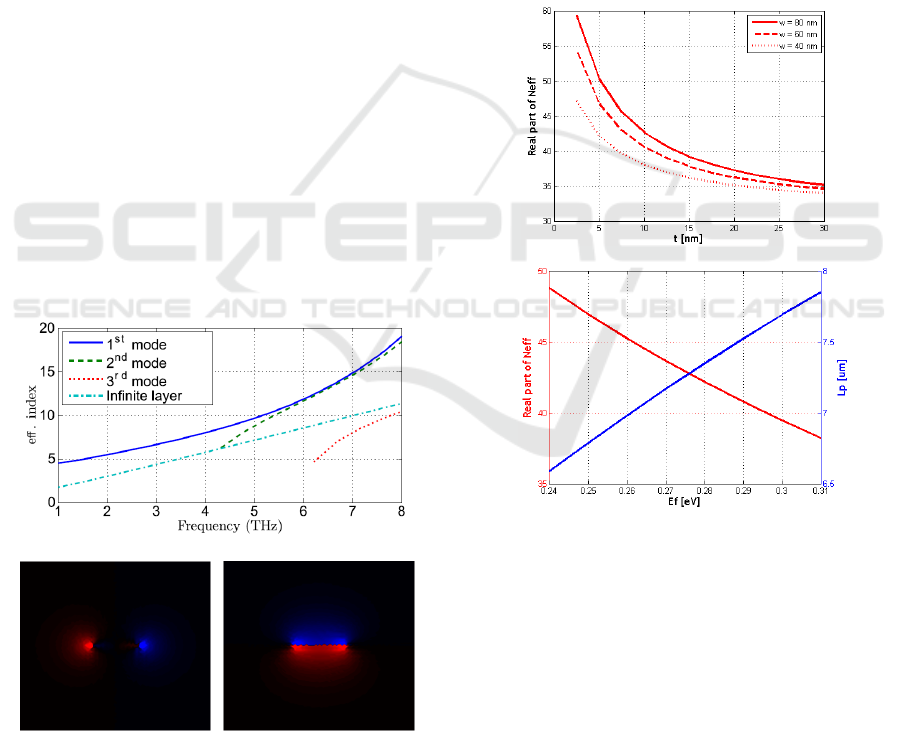
structures (Figure 1).
Figure 1: Representation of graphene as an infinitely thin
sheet (2D cross section) and its surrounding surface.
Analysis and Design of Hybrid and Graphene-Based Plasmonic Waveguide Components
25

A first route to incorporate graphene sheets in
FEM simulations is to start from a bulky material
approach and consider the limit of its thickness to
zero. In this case, graphene’s contribution would be
apparent through its conductivity, thus affecting the
3rd and 4th term of (2) which include permittivity
quantities. In these integrals, separating a finite
surface of thickness
corresponding to the bulky
graphene area, we derive the additional terms
11
22
0 , 0 ,
g t r tt t z r zz z
SS
I k ds k E E dsEE
(6)
where we replace the permittivity with the complex
permittivity of graphene
*
0
/
r r b
j
, and
b
describes an equivalent conductivity of bulk
graphene (in S/m). Assuming that
b
consists of
non-zero real and imaginary parts, we can omit
r
as being included in
b
and have
*
0
/
rb
j
.
Therefore (6) becomes
11
0 0 0 0
g t b t z b z
SS
I jk ds jk E E dsEE
(7)
Assuming an infinitesimal graphene thickness,
variations are negligible in this dimension, giving
0 0 , , 0 0
g t p g t p z g z
SS
I jk dl jk E E dlEE
(8)
where
b
equals the surface conductivity
g
(in
S). It has to be particularly noted that the electric
field component
,tp
E
involved in the first integral is
not the full transverse component but only its
tangential projection on the one-dimensional
graphene line.
An equivalent and more elegant way to arrive at
the same expression is to consider graphene as a
zero thickness sheet in the first place. In this case,
the line integral term in (2) cannot be ignored, as the
graphene current sheet introduces a discontinuity in
the magnetic field, thus affecting the line integral
term. In particular, the interface condition on the
graphene sheet is written in the form
00
,
ˆˆ
ˆ
gg
s g t p z
j
k
E
n E n E
J E z
(9)
where
ˆ
g
n
is the unit vector normal to the graphene
sheet. However, to substitute (9) in the line integral
term of (2) we need to consider a fictitious surface
that surrounds the graphene sheet from both sides
and being infinitely close to it. Therefore, the line
integral is split into two parts, one for the upper
surface, where the outward-pointing unit normal
vector is
ˆˆ
g
nn
and one for the lower one, where
ˆˆ
g
nn
and the line integral takes the form
00
ˆˆ
ˆ
g
SS
g
S
gp
S
I ds ds
ds
jk ds
E n E E n E
E n E E
EE
(10)
which easily results in (9) as well.
Therefore, graphene’s contribution can be
implemented by adding two line integral terms in the
initial formulation, expressed as
, ,g
,,
,
t g z
e t p g t p e z g z
CC
T dl T E E dlEE
(11)
and by considering the corresponding matrices, it
results in the linear eigenvalue problem similar to
(5), where the term
,
00
tg
jk T
is added to
2
0
tt
kST
and
z,
00
g
jk T
is added to
,2
0
z m z
kST
.
The three-dimensional FEM formulation is
similarly based on a standard Galerkin formulation
with vector finite elements in three dimensions,
starting from the 3D version of (2). Since there is no
split in transverse and axial components, the
Galerkin formulation will include only 3D forms of
the first, third and last terms in (2). Following
similar principles, a graphene-raleted term of the
form
00
g
jk T
will be added to the standard FEM
stiffness-mass matrix
2
0
kST
.
3 PLASMONIC AND SWITCHING
COMPONENTS
The proposed formulations are is able to analyze
both plasmon graphene ribbon waveguides in the
THz regime and a switching-capable waveguide
structure for telecom applications, based on the CGS
waveguide (Dai and He, 2009), which is properly
enhanced by graphene.
Fourth International Conference on Telecommunications and Remote Sensing
26
3.1 Graphene waveguide with high-
index dielectric ridge
The first structure simulated was the graphene
waveguide proposed in (Sun et al., 2014). Its
concept takes advantage of a high-index dielectric
ridge to achieve strong field confinement without
using a finite width graphene ribbon which is harder
to fabricate. Placing a wide graphene sheet over a
dielectric ridge of appropriate size, the geometry of
the structure facilitates waveguiding. The relation of
the complex effective refractive index to the
thickness of gap the graphene sheet and the
dielectric ridge, as well as to the chemical potential
are shown in Fig. 3, being in very good agreement
with (Sun et al., 2014).
3.2 Graphene microribbon waveguide
To fully test the functionality of our formulation, we
analyzed a plasmon graphene microribbon
waveguide in the THz regime (Nikitin et al., 2011).
This is a waveguiding structure for frequencies
between 1 and 12 THz (as opposed to the
telecommunications wavelength regime) taking
advantage of the surface conductivity of a graphene
microribbon. The analysis was conducted for a
ribbon width of 5 um and the electric field intensity
plots for the two transverse components are shown
in Figure 2.
Figure 2: Effective refractive index (real part) and mode
profiles for the first mode of a 5um graphere ribbon
waveguide (vertical and horizontal E-field component,
respectively).
3.3 Graphene waveguide with high-
index dielectric ridge
The next structure simulated was the graphene
waveguide proposed in (Sun et al., 2014). Its
concept takes advantage of a high-index dielectric
ridge to achieve strong field confinement without
using a finite width graphene ribbon which is harder
to fabricate. Placing a wide graphene sheet over a
dielectric ridge of appropriate size, the geometry of
the structure facilitates waveguiding. The relation of
the complex effective refractive index to the
thickness of gap of the graphene sheet and the
dielectric ridge, as well as to the chemical potential
are shown in Figure 3, being in very good agreement
with (Sun et al., 2014).
Figure 3: Real part of the effective refractive index with
respect to gap thickness and chemical potential
3.4 Graphene switching component
Based on the analysis, we propose a switching
capability for the classic plasmonic CGS waveguide
(Dai and He, 2009), (Wu et al., 2010) by adding
graphene layers on all interfaces between waveguide
materials, including both sides of the oxide layer,
and also the two vertical ridges of the waveguide.
The ON and OFF states of the waveguide
correspond to chemical potential values 1 eV and 0.1
eV. Selecting a structure length of 10 um, the
insertion loss can be as low as 2.15 dB, almost
Analysis and Design of Hybrid and Graphene-Based Plasmonic Waveguide Components
27
entirely due to metal (not graphene) losses and the
achieved extinction ratio is 8.6 dB, which is highly
promising for further study.
3.5 Switched plasmonic components
with frequency selective
finctionalities
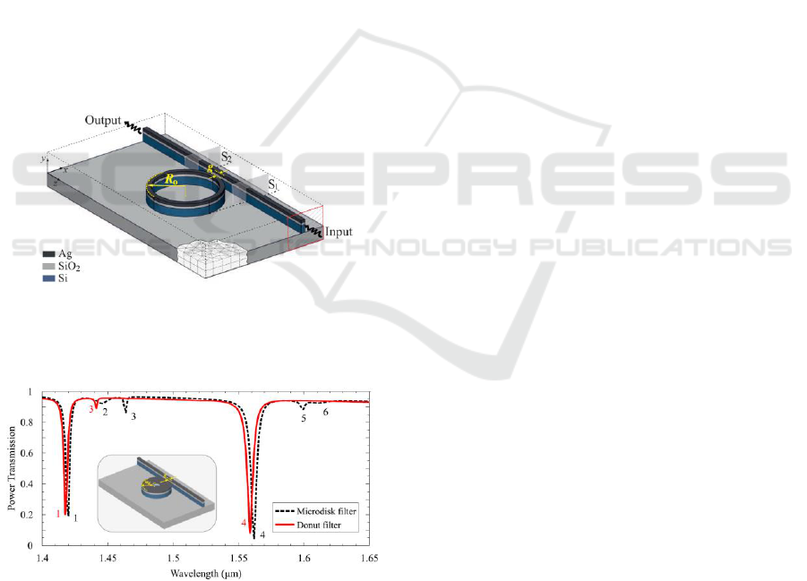
Following the proposed waveguide components we
further proceed to the design of three dimensional
components with frequency tuning functionalities,
like the waveguide-coupled microring structure of
Figure 4. For more enhanced performance, the
microring concept is extended to cover the cases of a
micordisk or a donut-shaped ring. The component's
performance, in terms of the power transmission
coefficient is shown in Figure 5, for both the
microdosk and donut shapes, for the ON state, while
the achieved extinction ratio between ON and OFF
states for the graphene enhanced component exceeds
11.5 dB, which is a figure suitable for practical
considerations.
Figure 4: Microring resonator filter based on the CGS
waveguide
Figure 5: Frequency response of the microdisk and donut
structures, in terms of the power transmission coefficient.
Outer ring radius is 0.85 um, inner ring radius for the
donut structure is 0.45 um and the gap is set to 150 nm.
4 CONCLUSIONS
We have presented a full-vectorial finite element
formulation for the eigenmode analysis of graphene-
based plasmonic waveguides and components with
switching functionalities. The formulation addresses
graphene as a surface conductivity thus eliminating
the need for fine discretizations inside thin graphene
sheets. Finally, several plasmonic or switched
components with promising characteristics have
been proposed.
REFERENCES
Bludov, Υ.V., Ferreira, Α., Peres N. M. R. and
Vasilevskiy M. I., “A Primer on Surface Plasmon-
Polaritons in Graphene,” Int. J. Mod. Phys. B, 27,
1341001, 2013.
Nikitin, A. Y., Guinea, F. and García-Vidal, F. J, “Edge
and waveguide terahertz surface plasmon modes in
graphene microribbon,” Phys. Rev. B, 84, 161407(R),
2011.
Sun, Y., Zheng, Z., Cheng, J. and Liu J., “Graphene
surface plasmon waveguides incorporating high-index
dielectric ridges for single mode transmission,” Optics
Communications, 328, pp. 124–128, 2014.
Selleri, S., Vincetti, L., Cucinotta, A. and Zoboli, M.
“Complex FEM modal solver of optical waveguides
with PML boundary conditions,” Optical and
Quantum Eletronics, vol. 33, no. 4-5, pp. 359-371,
2001.
Dai, D. and He, S., “A silicon-based hybrid plasmonic
waveguide with a metal cap for a nano-scale light
confinement”, Optics Express, vol. 17, no. 19, 2009.
Wu, M., Han, Z. and Van, V., “Conductor-gap-silicon
plasmonic waveguides and passive components at
subwavelength scale,” Optics Express, vol. 18, no. 11,
pp. 11728-11736, 2010.
Fourth International Conference on Telecommunications and Remote Sensing
28
