
New Fabrication Method of Plastic Micro-Lens Arrays for
Researching on Compound Eyes of Insects
Toshiyuki Horiuchi and Ryunosuke Sasaki
Tokyo Denki University, 5 Senju-Asahi-cho, Adachi-ku, Tokyo, Japan
Keywords: Compound Eye, Micro-Lens Array, Projection Exposure, Epoxy Resin, Resist Mold.
Abstract: To develop artificial compound eyes, sizes of element lenses of typical insects were actually investigated, and
a new simple and low-cost method for fabricating plastic micro-lens arrays was developed. It was thought
essential to research on artificial compound eyes that lens parameters were freely controllable by our minds.
For this reason, a new easy and low-cost fabrication method had to be developed. In the new method, original
molds of micro-lens arrays with concave profiles were formed lithographically in a thick resist film. The
concave resist patterns were printed using a handmade 1/19 reduction projection exposure system by only one
exposure. Using intentionally defocused exposure, curvature radiuses were controllable in a very wide range
of 21-85 μm for the same transparent hexagon patterns with an inscribed circle diameter of 26.3 μm. It was
also verified that the resist-mold patterns were faithfully replicated to epoxy resin. After pouring the liquid
resin onto the silicon wafer chip with resist-mold patterns, hardened solid resin with micro-lens arrays was
separated from the wafer chip by peeling off the wafer chip mechanically. It is promising to fabricate micro-
lens arrays with aimed lens parameters although some more subjects should be cared from now on.
1 INTRODUCTION
Human beings have been imitating distinguished
functions of other living things, and invented various
apparatuses exercising performances superior to the
original ones. Recently, biomimetic technologies
utilizing exquisite functions or special organs of small
insects or protozoa are drawing attension for
improving our lives or curing some diseases of our
organs. For example, structures of morpho-butterfly
are utilized for obtaining highly reflective surfaces
with beautiful blue colors in wide view angles (Neu
et al., 2015) (Saito et al., 2004). Hydrophobic surfaces
are researched by getting hints from wrinkles of
living things (Bowden et al., 1998) (Genzer and
Groenewold, 2006). Flapping flight technology
reffering to insects are also researched for developing
light and small flying robots (Maet al., 2013).
Organs that the authors are especially interested
are compound eyes of insects. They are excellent
optical systems that humans are not equipped, and a
lot of very interesting papers were published (Chen et
al., 2011) (Ogata et al., 1994) (Sanders and Halford,
1995) (Cao et al., 2015) (Li et al., 2013) (Tanida et
al., 2001) (Duparré et al., 2006) (Jeong et al., 2006)
(Jiang et al., 2015). Compound eyes are highly
precise optics using micro-lens arrays, and new
applications will probably be found in the future
besides ordinary usage as eyes.
To start researches on compound eyes, it was
thought preferable to possess technology for
fabricating micro-lens arrays with various lens
parameters such as diameters and curvature radiuses
by ourselves easily. For this reason, a new fabrication
method of plastic micro-lens arrays is investigated
here.
2 SURVEYS ON SIZES OF LENS
ARRAYS
Compound eyes have been eagerly researched in the
world, and artificial compound eyes have also been
reported (Ogata et al., 1994) (Tanida et al., 2001)
(Duparré et al., 2006) (Li et al., 2013). Accordingly,
typical sizes of micro-lens arrays are known.
However, in the first step, it is preferable that actual
examples are easily obtained, and they are easily
observed for imitating them. For this reason,
compound eyes of cicada, dragonfly and goldbug
were in fact investigated. Outlooks of insects and
magnified photographs of their compound eyes are
shown in Figures 1-3.
40
Horiuchi, T. and Sasaki, R.
New Fabrication Method of Plastic Micro-Lens Arrays for Researching on Compound Eyes of Insects.
DOI: 10.5220/0005666900400047
In Proceedings of the 9th International Joint Conference on Biomedical Engineering Systems and Technologies (BIOSTEC 2016) - Volume 1: BIODEVICES, pages 40-47
ISBN: 978-989-758-170-0
Copyright
c
2016 by SCITEPRESS – Science and Technology Publications, Lda. All rights reserved
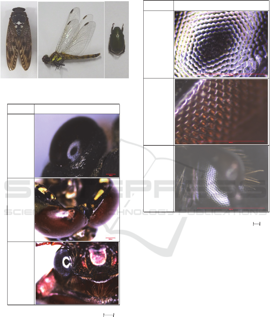
Figure 1: Insects whose compound eyes were investigated.
Figure 2: Photographs of compound eyes of insects.
All of investigated compound eyes were composed of
micro-lenses arrayed in dense hexagonal arrangement
like a honeycomb. Typical widths of the element
hexagons or the inscribed circle diameters of element
lenses were 33, 53, and 16 μm, respectively. For, this
reason, sizes of fabricating micro-lenses were
Figure 3: Magnified view of compound eyes of insects.
tentatively fixed to around above diameters, and a
new simple and easy method for fabricating plastic
lens arrays was investigated. It was considered that
the lens parameters such as diameters, pitches, and
curvature radiuses should be widely controllable to
increase the facility of optical designs. In addition,
lens arrays should be fabricated by researcher
ourselves according to necessary specifications.
Regrettably, roundness or curvature radiuses of the
micro-lenses were not detectable. However, lens
characteristics are defined by both side curvatures of
the lens. In addition, the medium behind the lens is
not air but organic materials. Accordingly, refraction
characteristics of the lens are not decided only by the
curvature radius of the lens surface. For this reason, it
was thought that measurement of the lens surface
curvature was not necessarily required on this stage.
500 μ
m
Cicada
Goldbug
Insect
Outlook of compound eye
Dragonfly
Cicada
Dragonfly
Goldbug
Insect
Magnified view of compound eye
50 μm
(b) Dragonfly
(c) Goldbug
(a) Cicada
New Fabrication Method of Plastic Micro-Lens Arrays for Researching on Compound Eyes of Insects
41
3 NEW FABRICATION METHOD
OF MICRO-LENS ARRAYS
Various fabrication methods of micro-lens arrays
have already been developed in the world.
Representative methods are ink-jetting (Zhu et al.,
2015) (Luoa et al., 2013) (Voigt et al., 2011) (Kim et
al., 2011), etching (Chen et al., 2010) (Deng et al.,
2012), grey scale lithography (Wu et al., 2002)
(Kuang et al., 2009) (Yang et al., 2007), laser tracking
(Wang, 2005) (Chiu and Lee, 2011), heat reflow
(Cheng et al., 2010) (Liu et al., 2010) (Pan and Su,
2007), and others.
However, It was thought that fundamental lens
parameters such as sizes and curvature radiuses
should be in suit with those of actual compound eyes
in the first step. In addition, it was considered that it
was preferable that various lenses were easily
purveyed for the research with a low cost. For this
reason, simple and low-cost fabrication method of
plastic lens arrays was reseached here.
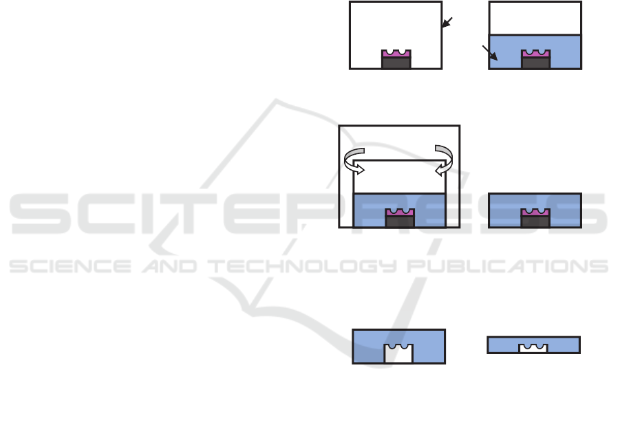
The new method investigated in this research is
shown in Figure 4. At first, original resist-mold
patterns were lithographically formed on silicon
wafers using a handmade 1/19 reduction projection
exposure system (Hirota et al., 2003). Concave resist
patterns were printed by intentionally exposing the
resist under large defocus conditions. By applying
such defocused exposure, smoothly distributed light
intensity profiles were given to the resist films even
using binary reticles with only transparent and opaque
parts and without gray tone parts. After forming the
resist-mold patterns, the wafer was cut in small chips,
and each silicon wafer chip with resist patterns was
fixed at the bottom of a paper cup using a piece of
both-side adhesive tape, as shown in Figure 4(a).
In the next step, a plastic resin was poured on
the resist-mold patterns, as shown in Figure 4(b).
Epoxy resin (Nissin Resin, Crystal Resin NEO) was
used here. After adding a material for hardening the
resin to the main epoxy resin, they were mixed using
a mixing machine with a function of removing air
bubbles (Thinky, AR100), as shown in Figure 4(c).
This time, thicknesses and sizes of the resin blocks
were roughly controlled by the cup diameter and the
poured resin volume. Because the lens characteristics
are influenced by the lens block thickness, however,
the thickness should be strictly controlled in the next
research step.
After the resin block was sufficiently hardened, it
was taken out from the cup, as shown in Figure 4(d),
and the wafer chip with resist patterns was forcibly
peeled off. In concrete, grooves were dug along the
wafer chip edges using a cutter knife, and the wafer
chip was lifted up by climbing a tip of tweezer under
it. As a result, the resin block with profiles inverting
the resist-mold profiles was obtained, as shown in
Figure 4(e).
Convex plastic lens patterns obtained by peeling
the wafer chip off had defects of remained resist
fragments. For this reason, the resist fragments were
removed by dipping the resin block in acetone for a
short while.
Finally, the resin block was thinned by polishing
it. As a result, finished resin plate with micro-lens
arrays were obtained, as shown in Figure 4(f).
Figure 4: New fabrication method of micro-lens arrays.
Because lens sizes and profiles are decided by the
reticle pattern size and the exposure conditions for
forming the original resist patterns, it is expected that
lens parameters are variously and widely changeable
suiting to optical designs.
(b) Pour of epoxy resin.
(a) Wafer chip fixed at the
bottom of a paper cup.
(c) Mixing of hardening
agent and resin. Bubbles
were removed
simultaneously.
(d) Resin block hardened
and taken out of the
paper cup.
(e) Resin block after
removing the wafer
chip.
(f) Finished micro-lens
array plate.
Paper
cup
Liquid
resin
BIODEVICES 2016 - 9th International Conference on Biomedical Electronics and Devices
42
4 EVALUATION OF RESIST
MOLDS AND RESIN LENSES
4.1 Conditions for Printing Concave
Resist-mold Patterns
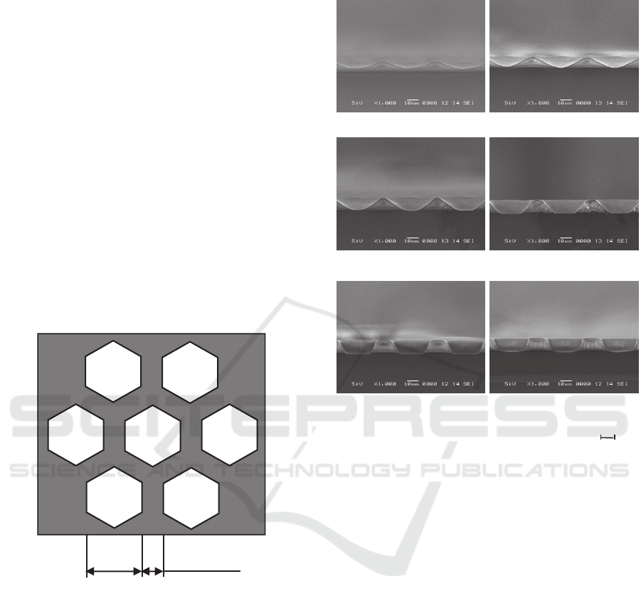
Micro-lens arrays were actually fabricated, and cross
sections and bird’s view profiles were evaluated. As
a resist, positive PMER P-LA900PM (Tokyo Ohka
Kogyo) was used, and the resist was coated on silicon
wafers in a thickness of approximately 10 μm.
Because actual compound eyes were hexagonally
arrayed, reticles shown in Figure 5 were used. The
width of transparent hexagon was fixed to 500 μm.
Because the reduction ratio was 1/19, the hexagon
width corresponds to the width of 26.3 μm on the
wafer plane, and this width almost corresponds to the
element lens diameter of cicada’s compound eye. On
the other hand, opaque boundary widths between
transparent hexagons were changed to 400, 300, and
200 μm.
Figure 5: Reticle patterns used for printing resist-mold
patterns of micro-lens arrays.
4.2 Evaluation of Resist-mold Patterns
At first, the best focal position or the focal origin was
decided as the stage position at which the sidewall
profiles of resist patterns became most perpendicular
to the wafer surface. Concave patterns with favorite
circular cross section profiles were obtained at the
defocus of +150 μm, as shown in Figure 6. Here, “+”
means that the exposed wafer was lowered down
from the projection lens. Concave patterns became
rounder and more circular in “+” direction than “-”
direction. Numerical aperture (NA) of the projection
lens was set at 0.12. Photographs of cross sections
were taken using a scanning electron microscope
(JEOL, JSM-5510).
Figure 6: Cross section variations of resist-mold patterns
under various defocus conditions.
Next, exposure time was varied to investigate the
relationship between the element lens profiles and the
exposure dose. In the experiments to decide the focal
origin by observing cross sections, it was very
difficult to break wafer chips at the exact center of the
concave resist patterns. For this reason, cross section
profiles under various exposure conditions were
evaluated using a laser microscope (Keyence, VK-
8510). Using the laser microscope, bird’s-eye views
were also obtained in addition to cross section
profiles.
At first, cross section profiles of resist-mold
patterns were measured. To evaluate cross section
profiles, they were pasted on screens of CAD
(Computer Aided Design) program (Autodesk,
AutoCAD 2014), and circles were delineated
superimposing on the cross section profiles by
defining the circles as they pass the concave bottoms
and both ends of the circular parts, as shown in Figure
7. By these manipulations, curvature radius R,
maximum profile error from the delineated CAD
circle δ, and concave depth d defined in the figure
were investigated.
500
μ
m 200-400
μ
m
+250 μm
+200 μm
+150 μm +100 μm
+50 μm 0 μm
10 μm
New Fabrication Method of Plastic Micro-Lens Arrays for Researching on Compound Eyes of Insects
43

Figure 7: Evaluated lens parameters of resist-mold patterns.
Figure 8: Wide variety of concave resist-mold patterns
when opaque pattern widths between transparent hexagonal
patterns and exposure doses are changed.
Dependence of circular radius R on exposure dose
is shown in Figures 8 and 9. Exposure dose of 384
mW/cm
2
corresponds to exposure time of 10 min. It
was clarified that the curvature radius was not almost
influenced by the opaque pattern width. This
characteristic is very convenient for designing reticles
to be prepared for fabricating micro-lenses with
aimed curvature radius. It was clarified that profiles
of resist-mold patterns were widely controllable by
changing exposure dose and opaque boundary width
between transparent hexagons, as shown in Figures 8
and 9.
Next, dependence of concave depth d is shown in
Fig. 10. In contrast to circular radius R, the concave
depth d varied depending on both exposure dose and
opaque pattern width between transparent hexagons.
The reason why the concave depths decreased for
reticles with narrow opaque parts is probably because
the resist at the opaque positions are exposed doubly
by light rays through transparent hexagons on both
sides, and slightly sensitized by the defocused
exposure. Therefore, the resist thicknesses of opaque
parts are also decreased during the development.
On the other hand, maximum profile error δ from
circular profiles are shown in Fig. 11. Although errors
became somewhat large under relatively large
exposure dose conditions, they were small, and it was
clarified that almost circular resist profiles were
obtained. Errors of 0.1 μm was the read out limit of
the used microscope.
Figure 9: Curvature radius dependence on exposure dose.
Curvature radiuses are not almost influenced by opaque
pattern widths between transparent hexagonal patterns.
R: Curvature radius
δ: Curvature profile error
d: Concave depth
R
δ
d
BIODEVICES 2016 - 9th International Conference on Biomedical Electronics and Devices
44
Figure 10: Concave depth dependence on exposure time
and opaque pattern width between transparent hexagonal
patterns.
Figure 11: Profile error dependence on exposure time and
opaque pattern width between transparent hexagonal
patterns. Detection limit of profile error was approximately
0.1 μm.
4.3 Replication to Plastic Resin
Because technologies for fabricating resist mold
patterns were almost fixed, replication to plastic resin
was investigated next. That is, feasibility of
separating a wafer chip with resist patterns and a resin
block was investigated, and replicated plastic lens
profiles were compared with the original resist-mold
patterns.
Resist-mold patterns were formed by adding
exposure dose of 230 mJ/cm
2
(exposure time of 6
min). Bird’s-eye views of resist-mold patterns and
replicated plastic lens profiles are shown in Figure
12(a) and Figure 12(b). It was clarified that resist-
mold profiles were almost faithfully replicated to the
resin. In Figure 13, cross sections of resist-mold
patterns and resin lens patterns are compared. It is
known that both cross section profiles are almost the
same though they are symmetrically formed.
Measured curvature radiuses, depths and profile
errors were compared, as shown in Table 1.
Finally, because the hardened resin blocks were
too thick, they were thinned down by polishing.
However, it took very long times to thin the blocks,
and it was very difficult to control the final
thicknesses. It is necessary to develop a better method
to thin the lens plate precisely without spending long
times from now.
(a) Resist-mold patterns replicated by an exposure dose of 230
mJ/cm2 using opaque patterns with a width of 200 μm. The scale
mark of 20 μm is effective only in horizontal direction. Concave
depths are displayed by colors.
(b) Micro-lens pattern finally replicated to epoxy resin.
Figure 12: Comparison of resist mold patterns and faithfully
replicated epoxy micro-lens patterns.
New Fabrication Method of Plastic Micro-Lens Arrays for Researching on Compound Eyes of Insects
45
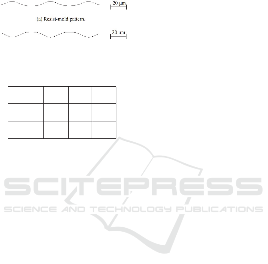
Figure 13: Comparison of profile curves between resist-
mold patterns and faithfully replicated epoxy micro-lens
patterns.
Table 1: Size differences between resist mold pattern and
resin lens pattern.
5 RATIONALITY OF CONCAVE
PATTERNING
Good balance of simplicity and accuracy of the new
method depend on the lithography process for
printing concave resist patterns. The key technology
is projection exposure under intentional large defocus
conditions.
In the past research, a similar method was used for
printing SU-8 patterns with vertical side walls and
very high aspect ratios (Hirota et al., 2003). In that
case, the negative resist SU-8 was a highly
transparent material, and the defocus was given for
making the widths of light intensity distribution
curves at the resist bottom equal to those at the resist
surface. However, in this paper, positive resist of
PMER P-LA900PM with large absorption was used,
and the pattern images were made vague even at the
surface. Using such translucent resist materials and
vague and gentle light intensity distributions, smooth
concave patterns with favourable quasi-spherical
profiles were obtained.
6 CONCLUSION
After investigating the typical compound eyes of
insects, plastic micro-lens arrays with similar lens
parameters were actually fabricated by developing a
new method. The aim is to prepare for developing
artificial compound eyes in the future. Because actual
element lens sizes of typical insects were in a range
of 16-53 μm, how to obtain micro-lens arrays with
such sizes simply and easily were investigated.
Various methods for fabricating micro-lens arrays
have already been proposed in the world. However, a
method that was simpler and more inexpensive was
necessary. In addition, it was preferable to make
possible to fabricate lens arrays by ourselves, and
change lens parameters such as diameters, curvature
radiuses and shapes freely.
In the new method, plastic micro-lens arrays were
fabricated by lithographically printing resist-mold
patterns, and faithfully replicating them to epoxy
resin. It was demonstrated that original concave resist
patterns were simply formed by only one lithography
process using intentionally defocused projection
exposure. In spite of the simplicity, curvature radiuses
of resist-mold patterns were widely controllable by
changing exposure dose. In addition, it was also
demonstrated that the resist-mold patterns were
faithfully replicable to epoxy resin by pouring the
resin onto the resist molds, and peeling a wafer chip
with the resist-mold patterns off mechanically after
the epoxy resin was hardened. Thus, convex lens
arrays of epoxy resin arranged in honeycomb styles,
and with an element shape of hexagon were
successfully fabricated.
There are still some subjects. The main subject is
the development of a better method for fabricating
lens arrays with precisely controlled thickness and
designed outline shapes. It is necessary to get down
to work hereafter.
ACKNOWLEDGEMENTS
This work was partially supported by Research
Institute for Science and Technology of Tokyo Denki
University, Grant Number Q15T-03.
REFERENCES
Bowden, N., Brittain, S., Evans, A. G. John et al., 1998.
Spontaneous formation of ordered structures in thin
films of metals supported on an elastomeric polymer,
NATURE 393 (1998) 146-149.
Resist-mold
pattern
Epoxy resin
pattern
Radius
(μm)
Depth
(μm)
Error
(μm)
32.4 4.2 0.1
31.3 4.1 0.1
BIODEVICES 2016 - 9th International Conference on Biomedical Electronics and Devices
46

Cao, Z., Zhai, C., Wang, K., 2015. Design of artificial
spherical super position compound eye, Optics
Communications 356, 218-222.
Chen, F., Liu, H., Yang, Q. et al., 2010. Maskless
fabrication of concave microlens arrayson silica glasses
by a femtosecond-laser-enhanced local wet etching
method, OPTICS EXPRESS 18, 20334- 20343.
Chen, H., Shen, X., Li, X., Jin, Y., 2011. Bionic Mosaic
Method of Panoramic Image Based on Commpound
Eye of Fly, Journal of Bionic Engineering 8, 440-448.
Cheng, H. C., Huang, C. F., Lin, Y. et al., 2010. Brightness
field distributions of microlens arrays using micro
molding, OPTICS EXPRESS 18, 26888-26904.
Chiu, C. C., Lee, Y. C., 2011. Fabricating of aspheric
micro-lens array by excimer laser micromachining,
Optics and Lasers in Engineering 49, 1232–1237.
Deng, Z., Chen, F., Yang, Q. et al., 2012. A facile method
to fabricate close-packed concave microlens array on
cylindrical glass, J. Micromech. Microeng. 22, 115026
(7pp).
Duparré, J., Dannberg, P., Schreiber, P., Bräuer, A., and
Tünnermann, A., 2005. Thin compound-eye camera,
APPLIED OPTICS 44 , 2949-2956.
Genzer, J. and Groenewold, J., 2006. Soft matter with hard
skin: From skin wrinkles to templating and material
characterization, Soft Matter 2 (2006) 310–323.
Hirota, K., Ozaki, M. and Horiuchi, T., 2003. Low-cost and
High-Performance Micro-Fabrication Method Using
Low Numerical-Aperture Optical Projection
Lithography on Copper-Clad Plastic Boards, Japanese
Journal of Applied Physics 42, 4031-4036.
Jeong, K. H., Kim, J., Lee, L. P., 2006. Biologically
Inspired Artificial Compound eye, Science 312, 557-
561.
Jiang, W., Hu, S., He, Y., Bu, Y., 2015. An artificial
compound eye of photon sieves, Optics & Laser
Technology 74, 93-96.
Kim, J. Y., Brauer, N. B., Fakhfouri, V. et al., 2011. Hybrid
polymer microlens arrays with high numerical
apertures fabricated using simple ink-jet printing
technique, OPTICAL MATERIALS EXPRESS 1, 259-
269.
Kuang, D., Zhang, X., Gui, M., and Fang, Z., 2009.
Hexagonal microlens array fabricated by direct laser
writing and inductively coupled plasma etching on
organic light emitting devices to enhance the
outcoupling efficiency, APPLIED OPTICS 48, 974-
978.
Li, F., Chen, S., Luo, H., Gao, Y., 2013. Curved micro lens
array for bionic compound eye, Optik 124,1346-1349.
Liu, K.H., Chen, M.F., Pan, C.T. et al., 2010. Fabrication of
various dimensions of high fill-factor micro-lens arrays
for OLED package, Sensors and Actuators A 159, 126–
134.
Luoa, Y., Wanga, L., Dinga, Y. et al., 2013. Direct
fabrication of microlens arrays with high numerical
aperture by ink-jetting on nanotextured surface, Applied
Surface Science 279, 36– 40.
Ma, K. Y., Chirarattananon, P., Fuller, S. B., Wood, R. J.,
2013. Controlled Flight of a Biologically Inspired,
Insect-Scale Robot, SCIENCE 340, 603-607.
Neu, S. et al., 2015. Excellent Structure-Based
Multifunction of Morpho Butterfly Wings: A Review,
Journal of Bionic Engineering 12, 170–189.
Niu, S., Li, B., Mu, Z. et al., 2015. Excellent Structure-
Based Multifunction of Morpho Butterfly Wings: A
Review, Journal of Bionic Engineering 12, 170–189.
Ogata, S., Ishida, J., Sasano, T., 1994. Optical sensor array
in an artificial compound eye, Optical Engineering, 33,
3649-3655.
Pan, C.T., Su, C.H., 2007. Fabrication of gapless triangular
micro-lens array, Sensors and Actuators A 134, 631–
640.
Saito, A., Yoshioka, S., Kinoshita, S., 2004. Reproduction
of the Morpho butterfly's blue: arbitration of
contradicting factors, SPIE 5526 (2004) 188-194.
Sanders, J. S., Halford, C. E., 1995. Design and analysis of
apposition compound eye optical sensors, Optical
Engineering, 34, 222-235.
Tanida, J., Kumagai, T., Yamada et al., 2001. Thin
observation module by bound optics (TOMBO):
concept and experimental verification, APPLIED
OPTICS, 40, 1806-1813.
Voigt, A., Ostrzinskia, U., Pfeiffer, K. et al., 2011. New
inks for the direct drop-on-demand fabrication of
polymer lenses, Microelectronic Engineering 88,
2174–2179.
Wang, S. Y., 2005. Computer simulation for the fabrication
of hexagonal micro lens arrays by use of the dragging
process with an excimer laser, OPTICS EXPRESS 13,
5600-5607.
Wu, H., Odom, T. W. and Whitesides, G. M., 2002.
Reduction Photolithography Using Microlens Arrays:
Applications in Gray Scale Photolithography,
Analytical Chemistry, 74, 3267-3273.
Yang, J. J., Liao, Y. S., Chen, C. F., 2007. Fabrication of
long hexagonal micro-lens array by applying gray-scale
lithography in micro-replication process, Optics
Communications 270, 433–440.
Zhu, X., Zhun, L., Chen, H. et al., 2015. Fabrication of high
numerical aperture micro-lens array based on drop-on-
demand generating of water-based molds, Optics &
Laser Technology 68, 23–27.
New Fabrication Method of Plastic Micro-Lens Arrays for Researching on Compound Eyes of Insects
47
