
High Perfomance Integrated Temperature Sensor based on
Amorphous Silicon Diode for Photonics on CMOS
Sandro Rao, Giovanni Pangallo and Francesco Della Corte
Università degli Studi “Mediterranea” - DIIES - Via Graziella Feo di Vito 89122, Reggio Calabria, Italy
Keywords: p-i-n diode, Temperature Sensor, Amorphous Silicon, Photonic Integrated Circuit.
Abstract: A temperature sensor based on a photonic layer-integrated hydrogenated amorphous silicon p-i-n diode is
presented. The linear dependence of the voltage drop across the forward-biased diode on temperature, in a
range from 30 °C up to 170 °C, has been used for thermal sensing. A high sensitivity of 11.9 mV/°C in a
biasing current range ≈34-40 nA has been measured.
1 INTRODUCTION
Hydrogenated amorphous silicon (a-Si:H) is a
promising platform enabling the desired matching
between electronics and on-chip photonics (Della
Corte, 2013). Thin layers of a-Si:H can be in fact
deposited using the CMOS-compatible low-
temperature plasma-enhanced chemical vapor
deposition technique (LT-PECVD), with no impact at
all on the microelectronic layers. Moreover, a-Si:H
could be deposited on different substrates where
crystalline silicon (c-Si) could not, be it a glass, a
metal, an already processed silicon wafer, or even
plastic.
Generally, on-chip temperature measurements are
explored for thermal variation compensation in many
sensing devices such as humidity, pressure, flow,
stress and gas concentration sensors (Mansoor, 2015).
Moreover, many Si-photonic active devices are
temperature-dependent, namely they are sensible to
the environment temperature variations due to the
large thermo-optic coefficient of Si. The thermal
sensitivity of the resonant wavelength for silicon ring
resonators is, i.e., of 100 pm/°C about (Yamada,
2011) or, to mention just another example, in a Mach
Zehnder (MZ) interferometer the TO effect is
responsible of a wavelength shift of 90 pm/°C
(Selvaraja, 2010). Consequently, such devices are not
practical without thermal compensation. Thermal
challenges need to be resolved in order to advance the
Silicon Photonics for future network-on-chip
interconnection systems.
In this work, a temperature sensor based on a
waveguide-integrated a-Si:H p-i-n diode is presented.
The linear dependence of the voltage drop across the
forward-biased diode on temperature variations from
T=30°C up to 170 °C has been accurately measured.
Similar sensors based on a-Si:H diodes were
already reported in literature showing however
sensitivities lower than 3.3 mV/°C in a temperature
range from T=30 up to 80 °C (De Cesare, 2015).
2 AMORPHOUS SILICON P-I-N
DIODE TEMPERATURE
SENSOR
The diode temperature sensor was integrated in
proximity to a Mach Zehnder interferometer (MZI),
Figure 1(a), and in particular close to the MZI arm
where the propagating optical signal phase shift is
achieved by electric-field induced p-i-n diode carrier
depletion. The schematic layout of the realized device
is shown in Figure 1(d) together with its geometrical
dimensions. More details about the MZI fabrication
are provided in (Rao, 2012).
The schematic cross section of the fabricated a-
Si:H waveguide vertical-integrated p-i-n diode is
shown Figure 1 (c). It consists of an intrinsic a-Si:H
layer, 2-μm-thick, between a p-doped a-SiC:H, 2-μm-
thick, and an n-doped a-SiC:H, 300-nm-thick. The p-
i-n cathode top contact is a 200-nm-thick Al layer.
The active area of device is 2.25·10
-4
cm
2
.
Rao, S., Pangallo, G. and Corte, F.
High Perfomance Integrated Temperature Sensor based on Amorphous Silicon Diode for Photonics on CMOS.
DOI: 10.5220/0005744903690372
In Proceedings of the 4th International Conference on Photonics, Optics and Laser Technology (PHOTOPTICS 2016), pages 371-374
ISBN: 978-989-758-174-8
Copyright
c
2016 by SCITEPRESS – Science and Technology Publications, Lda. All rights reserved
371
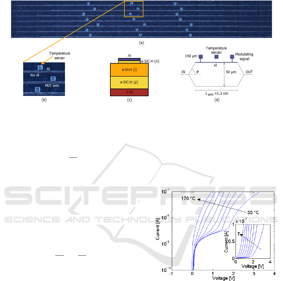
Figure 1: (a) A Optical microscope (top view) of the MZI a-Si:H based modulators and temperature sensors. (b) Top view
and schematic cross section (c) of integrated a-Si:H p-i-n diode temperature sensor. (d) Schematic MZI, plot not in scale.
As well-known, the I
D
current flowing in a p-i-n
diode at a given applied voltage V
D
can be analytically
described using the following formula:
1
kT
qV
SD
D
eII
(1)
where η is the ideality factor, I
s
is the saturation
current, q is the electric charge and k is the Boltzmann
constant.
The characterization of the sensor output has been
performed under forward bias condition where, at
constant DC current, the voltage across the diode is
linearly dependent on the temperature.
In fact, for qV
D
>>ηkT the voltage dependence on
temperature can be obtained from (1), yielding:
S
D
D
I
I
q
kT
V ln
(2)
Equation (2) makes explicit the linear dependence
V
D
-T as long as the non-linear contribution of Is can
be considered negligible with respect to I
D
.
3 EXPERIMENTAL RESULTS
In our setup, the p-i-n diodes have been biased with a
current I
D
kept constant in the whole temperature
range. The devices were tested in a climatic chamber
(Galli Genviro-030-C) setting the reference
temperature through its internal PID digital
microcontroller. A calibrated PT100 sensor, with an
accuracy of ±0.3 °C, was placed in contact with the
device under test in order to monitor, during the
measurements, the exact temperature set points
gradually varied from (to) 30 to (from) 170 °C.
The bias current I
D
was varied in a range from 1
nA to 100 nA and the corresponding voltage drop V
D
across the a-Si:H p-i-n diode was measured by using
the Agilent 4155C Semiconductor Parameter
Analyser. In Figure 2 we report the I
D
-V
D
characteristics, for different temperatures in a range
from 30 up to 170°C.
Figure 2: Forward Current-Voltage Characteristics for
Temperatures Ranging from 30 up to 170°C. the Inset
Shows a Detail of the I
D
-V
D
-T Characteristics in Linear
Scale.
From I
D
-V
D
-T measurements, the highly linear
dependence of the drop voltage across the p-i-n diode
on different temperatures have been extracted as
shown in Figure 3.
In our analysis, the coefficient of determination
(R
2
) has been calculated to evaluate the agreement
between the experimental measurements and their
linear best-fit, f
L
(T). In particular, R
2
allowed us to
quantify the sensor linearity goodness by fitting the
experimental data with a linear model.
AOMat 2016 - Special Session on Advanced Optical Materials
372
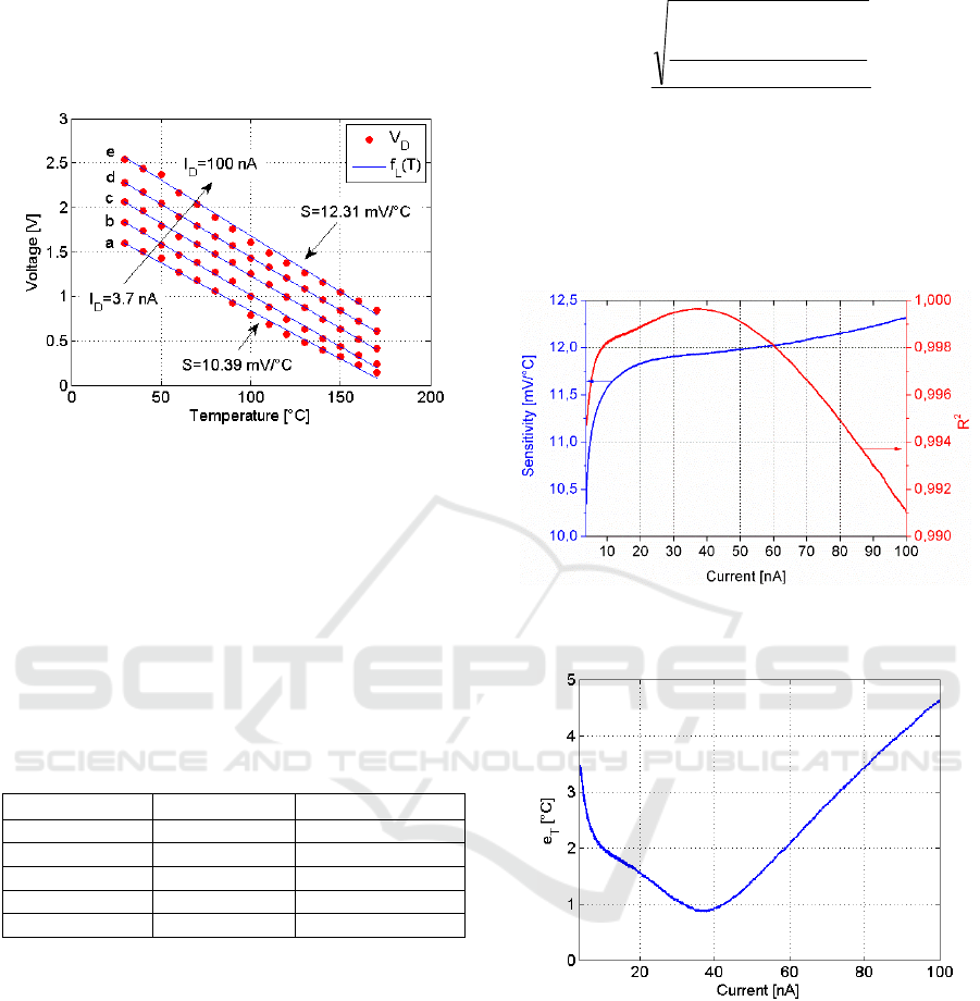
In the same figure, the measured data are fitted
with the best-calculated linear model showing a good
degree of linearity (R
2
>0.99) for the whole considered
range of I
D
, 3.7 nA to 100 nA.
Figure 3: Measured (points) forward voltages versus
temperature at different polarization currents. Experimental
data are fitted with the best-calculated linear model f
L
(T).
The sensor sensitivity, S, is defined as the
temperature derivative of equation (2) and, therefore,
it can be calculated from the slope of the V
D
-T
characteristics. The calculated values of S for the five
cases shown in the figure are reported in Table I.
For I
D
=3.7 nA the sensitivity is 10.39 mV/°C and
increases up to 12.31 mV/°C for I
D
=100 nA.
Table 1: Sensor sensitivity, S, calculated from V
D
-T
characteristics.
lines of Fig. 5 I
D
[nA] S [mV/°C]
a 3.7 10.39
b 38 11.9
c 52 11.99
d 76 12.12
e 100 12.31
A more detailed analysis of R
2
and S is shown in
Figure 4 for all values of I
D
in steps of 100 pA.
It is worth noting that the coefficient of
determination varies by only 0.25% from an average
of R
a
2
=0.9972 over the considered temperature range
leading to a temperature sensor with a highly linear
behavior in a wide range of biasing currents. The
maximum of R
2
~0.9996 has been calculated in the
current range ≈34-40 nA corresponding to a
sensitivity S=11.9 mV/°C.
To evaluate the mismatch between the calculated
linear best-fit, f
L
(T), and the experimental
measurements, the corresponding root mean square
error (rmse) was first calculated and subsequently
converted into a temperature error value using the
following formula:
S
n
TfTV
e
n
i
iLiD
T
1
2
))()((
(3)
where n is the number of the temperature set
points.
The calculated plot, e
T
versus I
D
, for the
considered temperature range is reported in Figure 5.
e
T
is always lower than 5 °C while the minimum
e
T
=0.87 °C is obtained for I
D
=37.3±3.3 nA.
Figure 4: Coefficient of determination and sensitivity
calculated for bias currents between I
D
=3.7 nA-100 nA.
Figure 5: r.m.s. error versus bias current.
4 CONCLUSIONS
A temperature sensor based on a waveguide
integrated a-Si:H p-i-n diode has been designed and
characterized. The linear dependence of the voltage
drop across the forward-biased diode on temperature,
in a range from 30° up to 170°C was demonstrated.
Measurements showed both a high degree of
linearity (R
2
=0.9996) and a high sensitivity (S=11.9
mV/°C) in the biasing current range ≈34-40 nA.
High Perfomance Integrated Temperature Sensor based on Amorphous Silicon Diode for Photonics on CMOS
373

Such devices can be integrated into photonic
integrated circuits (PICs) for sensing applications and
in CMOS compatible photonic active devices for
which the temperature variation is an issue.
REFERENCES
Della Corte, F.G. & Rao, S., 2013. Use of amorphous
silicon for active photonic devices. IEEE Transactions
on Electron Devices, 60(5), pp.1495–1505.
Mansoor, M. et al., 2015. Silicon diode temperature
sensors—A review of applications. Sensors and
Actuators A: Physical, 232, pp.63–74.
Yamada, S. et al., 2011. Experimental investigation of
thermo-optic effects in SiC and Si photonic crystal
nanocavities. Optics Letters, 36(20), pp. 3981.
Selvaraja, S. K. et al., 2010. Thermal trimming and tuning
of hydrogenated amorphous silicon nanophotonic
devices. Appl. Phys. Lett. 97, pp 071120
Be Cesare, G., Nascetti, A. & Caputo, D., 2015. Amorphous
Silicon p-i-n Structure Acting as Light and Temperature
Sensor. Sensors, 15(6), pp.12260–12272.
Rao, S. et al., 2012. A 25 ns switching time MachZehnder
modulator in as-deposited a-Si:H. Optics Express,
20(9), pp. 9351.
AOMat 2016 - Special Session on Advanced Optical Materials
374
