
Analysis and Simulation of Fault Tolerance of a Grid-connected PV
Inverter by Z-source Impedance
Diego P. Chacón-Troya
1
, Christian Jara Alvarez
1
, Enrique Galarza Pablo
1
and José Manuel Aller
1,2
1
Universidad Politécnica Salesiana, Cuenca, Ecuador
2
Universidad Simón Bolívar, Caracas, Venezuela
Keywords: Fault Tolerant Circuits, Z-source Inverter, MPPT, PV Panels.
Abstract: This paper proposes the design of a monophasic inverter connected to a residential network by applying Z-
Source topology. The proposed models were verified in normal operation “STC” and under short circuit
conditions “SC”. The system is presented as coupled to a network without a transformer and with minimum
electrical components. The tolerance of the overcurrent or short-circuit current is also analyzed on this
topology. The signal’s power is conditioned to find the MPP of the PV panels. Its architecture will be outlined,
described and simulated in Matlab’s Simulink®. In order to verify that the design is working properly.
1 INTRODUCTION
The failure analysis in power conversion equipment
has become a critical focus of study in different types
of industrial applications (Cordeiro et al, 2011; Tajfar
and Mazumder, 2012). Current developments for
photovoltaic installations connected to the grid, due
to factors such as declining costs of solar panels and
decentralized power generation, offer a greater
market potential, making them competitive with
conventional energy sources. Guaranteeing the
continual operation of the system is of vital
importance, therefore making the fault tolerance
analysis for this type of systems of vital importance
as well (Tajfar and Mazumder, 2012; Chavan and
Chavan, 2014).
Among the faults that can be found in power
converters are the electrolytic capacitors which are
very susceptible to fault in the systems. In order to
continue the order of importance, we have the
switching devices which groups the semiconductors,
the control circuit, the ceramic capacitors, the diodes
and the inductors (Chan-Puc et al, 2009).
These devices perform the photovoltaic energy
conversion using only electrical components which
increases operational longevity when functioning
correctly. The power converters being the most
vulnerable to faults according to reliability studies
(Petrone et al, 2008; Dhople et al, 2012), its capacity
for fault tolerance reduces unit degradation and
increases performance. However, its cost, weight, and
size make its operation increasing complex because
the system requires more components, making future
improvements to overall system performance a
challenge for the future, including aspects of lifetime
performance of the integrated components in order to
reduce losses and increase reliability (Cordeiro et al,
2011; Petrone et al, 2008; Tuan et al, 2012)
Connecting to the grid without the use of a
transformer is an increasingly popular alternative
where new topologies are studied in order to develop
solid state architecture, mitigate problems associated
with the galvanic connection between the grid and the
PV generator, and reduce size and wear (Tuan et al,
2012; Patrao et al, 2011).
As new power conditioning strategies are
proposed ZSource topology is of special note because
studies have shown that it increases conversion
efficiency by 1% compared with existing systems and
the inverter system by 1% to 15% in comparison to
conventional PWM inverters depending on their use
(Patrao et al, 2011; Meinhardt and Mutschler, 1995).
This article proposes a study of photovoltaic
generation connected to a residential grid, using a
simple fault tolerant topological system in order to
increase reliability in the VSI. As a method for
conditioning solar power, an innovative design is
attached to the inverter which is used to adjust the
voltage levels at the inverter input to maximize the
energy extracted from the solar panels, allowing a
connection to the grid without a transformer
324
Chacón-Troya, D., Alvarez, C., Pablo, E. and Aller, J.
Analysis and Simulation of Fault Tolerance of a Grid-connected PV Inverter by Z-source Impedance.
In Proceedings of the 5th International Conference on Smart Cities and Green ICT Systems (SMARTGREENS 2016), pages 324-329
ISBN: 978-989-758-184-7
Copyright
c
2016 by SCITEPRESS – Science and Technology Publications, Lda. All rights reserved
(Cordeiro et al, 2011). This design is known in
academic literature as ”Z inverter”. Its two inductors
connected in series between the DC source and
inverter allow the limitation of the di/dt variance of
the device, giving the system time to disconnect and
avoid damage or destruction of the system (Peng,
2003; Milady et al, 2009).
2 DEVELOPING
2.1 Z-source Topology
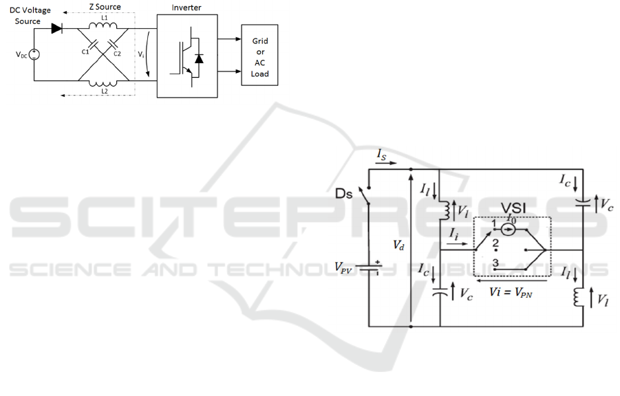
Figure 1: General configuration of a Z Source Inverter
(Hanif, Basu &Gaughan, 2011).
Its topology (Figure 1), allows the coupling between
the AC/DC inverter and the primary DC power source
through an LC filter forming an ”X” between two
inductors and two capacitors, usually with a smaller
capacity than those used in an equivalent
conventional converter, a diode then directs the DC
source current to flow only towards the load. With
this configuration, a short-circuit will not destroy the
system, compared with other types of power
converters, with Buck– Boost functioning stages in
the same device allowing the application of voltage
and current source inverters without needing to
change the system topology (Peng, 2003; Zope et al,
2010; Hanif et al, 2011).
2.2 Z- source Function
A conventional single-phase inverter has 4 operating
states, the Z inverter, allowing an additional
operational state called Short Through or ”ST”, the Z
Source Inverter has 5 operational states ”ZSI” are
classified by 3 operational modes, as detailed in
Figure 2 (Peng, 2003; Hanif et al, 2011):
1) Mode 1: The inverter is operating within normal
operational states, the current circulates through the
load, this mode is represented by an equivalent
circuit, represented by a current source as shown in
Figure 2 (1). The DC voltage source appears across
the Z-network inductor and capacitor. The capacitor
charges (kept in a charged steady state), the inductor
is discharged and energy flows through this to the
load (Zope et al, 2010; Hanif et al, 2011).
2) Mode 2: The Bridge AC / DC operates in zero
states, the higher or lower switches short-circuit the
charge through the device, leaving the load in open
circuit. Its equivalent circuit is a source of zero
amplitude current ”open circuit” as shown in Figure
2 (2). The DC source voltage appears across the
inductor and capacitor (Bost stage), no current flows
to the load (Zope et al, 2010; Hanif et al, 2011).
3) Mode 3: Running on ST inverter the switches short
the Z network, as shown in Figure 2 (3). The load
voltage is zero, the capacitor charge time (
) of the
ST required. This interval is inserted in the states zero
of mode 2, allowing the voltage boost whenever the
photovoltaic panel is unable to provide the required
voltage for any voltage drop due to changes in
temperature or insulation. It should be taken into
account that
2
, at this moment
the voltage in capacitors charges the inductors (Zope
et al, 2010; Hanif et al, 2011).
Figure 2: Equivalent circuits of Z Source Inverter
(Rajakaruna and Jayawickrama, 2010). (1) Mode 1, (2)
Mode 2 and (3) Mode 3.
2.3 Simple Boost Control (SBC)
MATH
The SBC method proposed by Peng (Peng, 2003), is
a control method for the ZSI based on traditional
PWM modulation where two horizontal reference
lines called
and
are added to the carrier signal
and modulation. These two reference lines are
compared with the carrier to generate the ST time of
the Z converter. These levels must be higher than the
amplitude modulation index, so that the ST mode
does not interfere with conventional single-phase
modulation PWM inverter. Limiting the ST value of
the modulation index and meets the condition
.
Analysis and Simulation of Fault Tolerance of a Grid-connected PV Inverter by Z-source Impedance
325
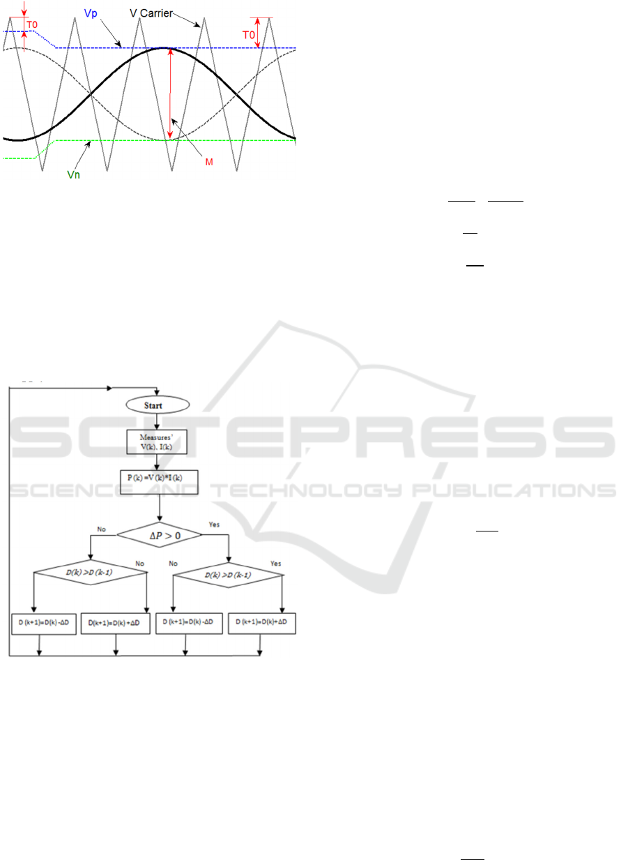
Figure 3: Switching time with “SBC” control method
(Zope, 2012).
2.4 Maximum Power Point Tracking
Strategy
The nonlinear characteristic of the photovoltaic
modules means that its maximum power point cannot
be reached by connecting directly to the load. For the
proposed system the P&O algorithm was been
chosen, a commonly used method, effective and easy
to apply.
Figure 4: MPPT P&O Algorithm (Rajakaruna and
Jayawickrama, 2010).
If the reference voltage
, in the PV array is
disturbed in one direction and the power produced by
the same increases, it means that the operating point
has moved to the MPP, therefore the operating
voltage must be moved in the same direction,
otherwise if the power extracted from the PV array
decreases, the operating point is moved in the
direction opposite the MPP location, therefore the
operating voltage must be moved in the opposite
direction, allowing the system to have a built-in signal
conditioning and connecting directly to the residential
grid, achieving maximum continuous power transfer
from the PV panel to the grid or to the load (Hanif et
al, 2011).
2.5 Modelling Z-Source
Assuming inductors 1 2 and capacitors 1
2, the mathematical equations that describe the
converter operating parameters for SBC Control Z are
(Hanif et al, 2011; Zope, 2012):
V
AC
=
MV
PN
2
=
M BV
PV
2
, (1)
T
0
=
B-1
2B
*T,
(2)
VC=
B+1
2
*V
PV
(3)
1) Design of Inductor: In normal operation of the
inverter mode 1, the inductor current decreases
linearly and its voltage is the difference between the
input voltage PV and the capacitor voltage. At this
point the input voltage appears in capacitors and a
small DC current flows through the inductors.
During mode 2 when operating in Buck – Boost
mode the function of the inductor is to limit ripple
current, and finally in the ST mode, or operating
mode 3, the current inductor increases linearly and the
voltage across the inductor is equal to the voltage
across the capacitor (Peng, 2003; Hanif et al, 2011;
Zope, 2012). According to these considerations the
inductance is calculated:
L=
V*T
0
∆L
(4)
is the maximum current in the inductor,
is the
minimum current in the Inductor
Where, ∆
and
is the time to ST
2) Capacitor Design: The function of the condenser is
to absorb the ripple current and to be able to stabilize
the voltage giving a quality sinusoidal wave to the
inverter output. The capacitor is charged during the
ST period, also as explained above in mode 3 the
current through the capacitor and inductor are equal
(Rajakaruna and Jayawickrama, 2010; Zope,
2012). In order to define the specifications of the
voltage ripple in the capacitor ∆, we must consider
a tolerance about 3% of the peak voltage according to
the specifications given in many applications where Z
converters have been designed (Rajakaruna and
Jayawickrama, 2010; Hanif et al, 2011). In this
manner, the condenser value could be estimated as:
∗
∆
(5)
SMARTGREENS 2016 - 5th International Conference on Smart Cities and Green ICT Systems
326
Where
is the ST period,
is the average current
through the inductor, and 4VC is considered 3% of
VC.
2.6 Modelling and Simulation
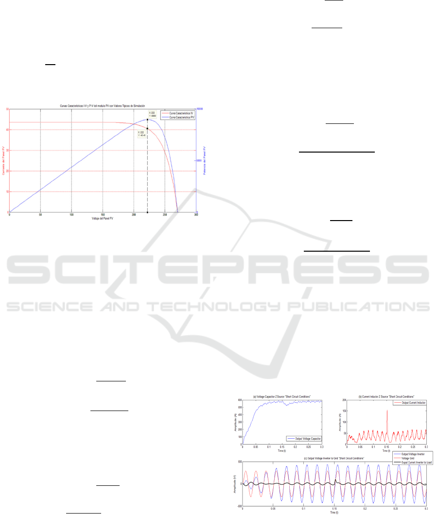
1) Characteristic PV Panel Curve: Considering the
standard operating conditions “STC” 25°;
1000
, the values of the photovoltaic panel
MPP are: Voltage 220,
40A Power 8800, as shown in Figure 5:
Figure 5: Characteristic curve PV Panel in "STC.
From the characteristic values of the PV panel the
maximum current through the Z inductor is obtained,
which corresponds to 30% of the average current
.
2.7 Modeling Z-source
To know the maximum boost factor B, it is necessary
to know the peak output voltage
294,
the
208, and the modulation factor
0,6,
230, using the equation (1):
B=
2V
AC
V
PV
*M
2 ∗ 294
220 ∗ 0,6
=4,45
For a frequency modulation of 10, the time
of ST according to the equation (2) is:
1
2
∗
4,45 1
2 ∗ 4,45
∗
1∗10
39,76μs,
It should be noted that the maximum
can be
inserted in mode 2 without any problem. The
maximum voltage the Z capacitor using equation (3)
is:
VC
B1
2
*V
PV
4,711
2
*230
599,5V.
The capacitor voltage provides the maximum values
supporting the DC bus and the switches of the inverter
bridge when in open circuit. With equation (4), the
value of the Z network inductance is calculated.
L=
VC*T
0
∆L
=
599,5
v
*39,76
us
24
≅1 mH,
To calculate the Z-source capacitor, use the Equation
(5).
C =
I
L
*T
0
∆V
C
=
40
A
*39,76
us
0,03*599,5
≅88,4 uF
The equations used for the analysis are
approximations of the Z converter and do not
consider factors such as transience due to switching,
resonant transience, or component resistances, so that
resonances not predicted in the design are occurring.
According to information obtained in literature (Zope
et al, 2010; Das et al, 2008; Shen et al, 2006
), the
converter stability output voltage can be increased by
a capacitor of1000.
Figure 6: Characteristic Curves of VZI in “STC”.
The AC output voltages connected to the network
shown in Figure 6 are very close to those calculated.
Analysis and Simulation of Fault Tolerance of a Grid-connected PV Inverter by Z-source Impedance
327
1) Fault Tolerance Test: When a short circuit occurs
in a conventional inverter “VSI” without Z network,
it produces a sudden change in current over time
/, as shown in Figure 7. A high current short-
circuit is generated in a short time putting the system
at risk, due to a delayed protection response which in
the best of cases produces strain on the components
or total destruction of the system.
Figure 7: Output of “VSI” in Short Circuit Conditions.
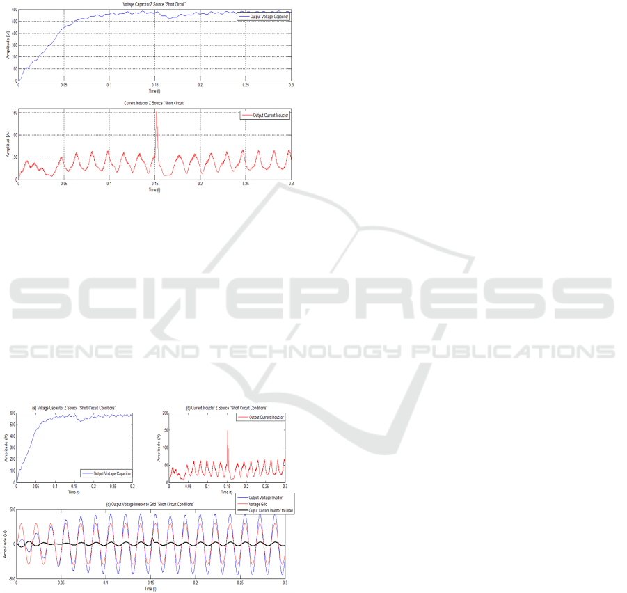
Upon the contingency of a short-circuit in the
proposed VZI system, as shown in Figure 8, the Z
network responds as we expected, attenuating the
variation /. This helps to allow the system
Protection the time needed to react without destroying
the enabled devices. In addition, if the failure is
dissipated before the protection activates, the inverter
can continue to operate normally as the Z network
does not allow the current to instantly rise to
destructive levels.
Figure 8: Ouput Waveforms from VZI “Short Circuit
Conditions”.
3 CONCLUSIONS
This paper proposes and analyzes a photovoltaic
system connected to the grid with a new fault-tolerant
topology.
The proposal combines an efficient topology fault
coverage, reduces stress on the components, and
increases the availability of power compared to
conventional photovoltaic inverter systems.
System behavior is analyzed via simulations in
STC and short circuit conditions, which reveals the
characteristic advantages offered by the Z Source
inverter. The results revealed that the Z network can
provide effective protection against short circuit,
decreasing the variation / in the system,
allowing enough time for the system protection to
intervene. With this feature, the system can withstand
short circuits without harming the operation or
performance of electronic devices.
This architecture is a good alternative for
applications in PV systems, for improving reliability
of these systems without increasing the number of
components and reducing the associated costs, and
improving the conversion efficiency of the inverter
compared to classical topologies.
REFERENCES
A. Cordeiro; J. Palma, J. Maia and M. Resende, 2011. Fault
tolerant design of a classical voltage-source inverter
using Z-source and standby redundancy, Electrical
Power Quality and Utilization (EPQU), 11th
International Conference,201, IEEE, pp. 1–6.
A. Tajfar, S. Mazumder 2012. A1 fault-tolerant switching
scheme for a high-power high-frequency-link inverter,
IECON 2012 - 38th Annual Conference on IEEE
Industrial Electronics Society, Oct 2012, pp. 5898–
5903.
F. Chan-Puc; H. Calleja, V. Sánchez, R. Acosta, and E.
Torres, 2009. Tendencias Actuales en el Diseño de
Convertidores de Potencia para Aplicaciones en
Fuentes de Energía Renovables, Revista de ingeniería
eléctrica, electrónica y computación, Diciembre 2009,
Vol. 7 No. 2.
S. B.Chavan and M. S. Chavan, 2014. Power switch faults,
diagnosis and tolerant schemes in converters of
photovoltaic systems a review, Department of
Electronic & Communication Technology, September
2014, vol. 3, Issue.
G. Petrone; G. Spagnuolo, R. Teodorescu, M. Veerachary,
and M. Vitelli, 2008. Reliability issues in photovoltaic
power processing systems, IEEE Trans Ind Electron,
July 2008, vol. 55, no. 7.
S. Dhople; A. Davoudi, A. D. Garcia, and P. Chapman,
2012. A unified approach to reliability assessment of
multiphase dc–dc converters in photovoltaic energy
conversion systems, Power Electronics, IEEE
Transactions, vol. 27, no. 2, pp.739–751.
M. Tuan; T. Wijnhoven, and J. Driesen, 2012. Fault-
tolerant topology of a grid-connected PV inverter
SMARTGREENS 2016 - 5th International Conference on Smart Cities and Green ICT Systems
328

coupled by a scott transformer, Conference on Power
and Energy, IPEC 2012, IEEE, pp. 428–433.
I. Patrao, E. Garcia, and F. González, 2011.
Transformerless topologies for gridconnected single-
phase photovoltaic inverters, Renewable and
Sustainable Energy Reviews, vol. 15, no. 7, pp. 3423–
3431.
M. Meinhardt and P. Mutschler, 1995. Inverters without
transformer in photovoltaic applications, http://www,
srt. tu-darmstadt, de/fileadmin/general/publicat/
meinepe.
F. Z. Peng, 2003. Z-source inverter, Industry Applications,
IEEE Transactions, vol. 39, no. 2, pp. 504–510,.
S. Rajakaruna and L. Jayawickrama, 2010. Steady-state
analysis and designing impedance network of z-source
inverters, Industrial Electronics, IEEE Transactions,
vol. 57, no. 7, pp. 2483–2491.
P. Zope; A. Patil, and A. Somkuwar, 2010. Performance
and simulation analysis of single-phase grid connected
pv system based on z-source inverter, Power
Electronics, Drives and Energy Systems (PEDES) &
2010 Power India, 2010 Joint International
Conference, pp. 1–6.
S. Milady; D. Silber, F. Pfirsch, and F. Niedernostheide,
2009. Simulation studies and modeling of short circuit
current oscillations in igbts, Power Semiconductor
Devices & IC’s, 2009. ISPSD 2009. 21st International
Symposium on IEEE, pp.37–40.
M. Hanif; M. Basu, and K. Gaughan, 2011. Understanding
the operation of a z-source inverter for photovoltaic
application with a design example, IET Power
Electronics, 2011,vol. 4, no. 3, pp. 278–287.
P. Zope 2012. Modeling and simulation of z-source inverter
design and control strategies, Ph.d., thesis, Electronics
and telecommunication engineering under the faculty
of engineering and technology, no. 3, pp. 22–28.
A. Das; D. Lahiri, and A. Dhakar, 2008. Residential solar
power systems using z-source inverter, TENCON 2008-
2008 IEEE Region 10 Conference.
M. Shen; A. Joseph, Y. Huang, F. Peng, and Z. Qian, 2006.
Design and development of a 50kw z-source inverter
for fuel cell vehicles, vol. 2, pp. 1–5.
Analysis and Simulation of Fault Tolerance of a Grid-connected PV Inverter by Z-source Impedance
329
