
Direct Observation of the 2D Gain Profile in High Power Tapered
Semiconductor Optical Amplifiers
Rebecca B. Swertfeger
1
, James A. Beil
1
, Stephen M. Misak
1
, Jeremy Thomas
2
, Jenna Campbell
2
,
Daniel Renner
2
, Milan Mashanovitch
2
and Paul O. Leisher
1,2,*
1
Rose-Hulman Institute of Technology, 5500 Wabash Ave, Terre Haute, Indiana, U.S.A.
2
Freedom Photonics, LLC., 41 Aero Camino, Santa Barbara, California, U.S.A.
Keywords: Semiconductor Laser, Diode Laser, Semiconductor Amplifier, Tapered Amplifier, Master-Oscillator Power-
Amplifier (MOPA), High Power, Beam Quality, Single-Mode, Gain Profile, Longitudinal Spatial Hole
Burning, Optical Communication Sources, Free-Space Optical Communication, InGaAsP, InP.
Abstract: A novel experimental approach to permit direct observation of the 2D gain profile in high power tapered
semiconductor optical amplifiers and integrated MOPA devices is reported. A two-dimensional simulation of
the photon, carrier, and gain distributions inside the tapered amplifier demonstrate gain saturation effects that
could be measured by directly viewing the spontaneous emission profile inside of the cavity. Tapered lasers
with a built-in window on the back of the device are fabricated and a SWIR microscope camera is used to
measure the spontaneous emission profile under operation at varying injection levels. The effect of gain
saturation due to stimulated emission is clearly observed and in close agreement with the theoretical model.
1 INTRODUCTION
Modest (watt-class) power levels and diffraction-
limited beam quality are required for a variety of
diode laser applications including optical
communication, narrow linewidth seeding, and
pumping. Conventional ridge waveguide lasers are
not capable of achieving these output levels due to the
low cross-sectional area (high series resistance) and
catastrophic optical mirror damage (in devices
operating at wavelengths below 1100 nm). For
optical communication applications, devices
operating around 1500 nm are particularly important.
Tapered diode laser master oscillator power amplifier
(MOPA) devices grown on InP substrates have shown
promise as a source of watt-class diffraction limited
optical power at 1550 nm (Donnelly, 1998) and
(Selmic, 2002).
The general concept of the tapered MOPA device
is as follows. Single-mode laser oscillation occurs
within the etched ridge waveguide laser region.
Optical power from this single-mode laser section is
then output into the mode expansion region, where
the fundamental Gaussian beam is free to expand due
to diffraction. A flared, or tapered, contact is
patterned in this region with an angle that is matched
to the natural diffraction angle of the injected beam.
This section operates above saturation intensity and
serves to efficiently amplify the signal. Because the
beam is free to expand, the cross-sectional area of the
device grows with position, keeping the peak
intensity much lower than would occur in a traditional
high power single-mode ridge waveguide laser
(promoting good reliability) and also greatly reducing
the thermal resistance of the device, allowing for
much higher power extraction than would be possible
in a traditional single-mode device. A schematic
drawing is shown in Figure 1.
In an ideal taper, the output optical mode from the
ridge region propagates along the length of the taper,
expanding (due to diffraction) to form a larger version
of the same mode. The mode is amplified as the
tapered region is pumped with electrical current,
leading to high optical output powers. For a fixed
taper angle, the longer the taper, the more the mode is
expanded and the higher the achievable output power.
114
Swertfeger R., Beil J., Misak S., Thomas J., Campbell J., Renner D., Mashanovitch M. and Leisher P.
Direct Observation of the 2D Gain Profile in High Power Tapered Semiconductor Optical Amplifiers.
DOI: 10.5220/0006187301140121
In Proceedings of the 5th International Conference on Photonics, Optics and Laser Technology (PHOTOPTICS 2017), pages 114-121
ISBN: 978-989-758-223-3
Copyright
c
2017 by SCITEPRESS – Science and Technology Publications, Lda. All rights reserved
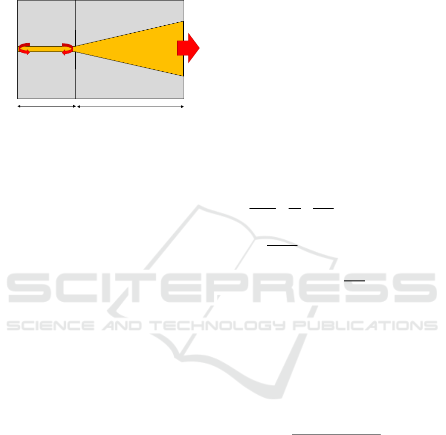
Figure 1: Schematic diagram of a single spatial mode
tapered master oscillator (MO) power amplifier (PA) laser.
In real tapered lasers, this ability to scale power while
maintaining single-mode performance is limited by
the stability of the lateral optical mode. The onset of
beam filamentation occurs in regions where the gain
is not well-saturated, such as along the edges of the
optical mode where the intensity is lower. Reflection
at the front facet creates a backwards-travelling wave
that can seed laser oscillation, especially in the
regions where the carrier density is high due to poor
gain clamping.
Because tapered amplifiers are edge-emitting
devices, typical measurement techniques do not
permit observation of the gain profile (though the
integrated amplified spontaneous emission can be
measured). In larger laser systems (solid state, fiber,
and gas lasers, for example), the gain can be measured
through the observation of the spontaneous emission
from the side of the laser cavity. High power tapered
semiconductor lasers, however, are bonded junction
down, and the excess solder that pools along the edge
of the device prevents investigation of the gain from
the side of the device. Thus, there exists a need for a
technique which allows for measurement of the gain
profile within the tapered amplifier, and the
demonstration of any such approach would greatly
benefit the development of tapered laser diodes.
In this paper, a method which permits direct
observation of the two-dimensional spontaneous
emission profile, and hence gain profile, within a
tapered optical amplifier is demonstrated. In the next
section, a model which accounts for coupling of the
photon density to the gain profile is developed. The
subsequent sections report the design of the device
and experimental results of the approach.
2 THEORY
2.1 Model Development
Modeling of the 2D photon and carrier distribution in
the tapered power amplifier was based on the
semiconductor laser rate equations and leveraged our
groups’ prior work modeling the effects of
longitudinal spatial hole burning in broad area
semiconductor lasers (Hao, 2014). The standard
semiconductor rate equations are modified to permit
variation of the local carrier density N(z), local
photon density
, and local gain
with
longitudinal position, as described in equations (1)
through (3) In a perfect optical amplifier, feedback
from the emitting facet (and cavity resonance) is
suppressed, thus it is only necessary to track the
forward propagating photon density.
(1)
(2)
(3)
The following parameters are defined as follows.
is the internal quantum efficiency, is the injection
current, and is the electron charge. is the volume
of the active region,
is the photons’ group
velocity, is the optical mode confinement factor,
is the intrinsic optical loss,
is the gain coefficient,
and
is the transparency carrier density. is the
carrier lifetime which includes Auger recombination,
Shockley-Read-Hall recombination, and spontaneous
radiative recombination (Chuang, 1995).
(4)
The finite difference method was used to solve the
simultaneous differential equations along the length
of the cavity. The length of the cavity was divided
into 50 steps and once the photon density was known
for the first point, it was calculated for the second, and
so on. This propagation process was repeated for
many steps in the width of the cavity so that a two-
dimensional model could be created.
Coupling of the photon population to the carrier
population results in an inverse relationship between
gain and photon density. Thus, as the injected signal
from the master oscillator is amplified along the z-
direction of the amplifier, gain and carrier density are
L
MO
L
PA
Single-Mode
Master Oscillator Tapered Power Amplifier
Direct Observation of the 2D Gain Profile in High Power Tapered Semiconductor Optical Amplifiers
115

necessarily reduced. Spontaneous emission, which is
proportional to the square of carrier density, is used
to extract the gain profile.
The two-dimensional distribution of gain is
calculated following a quasi 1D approach.
Fraunhofer far-field diffraction of the injected optical
mode is assumed, resulting in a linear divergence of
the fundamental Gaussian-like mode along the cavity
length. The diffraction angle is calculated from a 2D
cross-sectional effective index simulation of the
optical mode in the ridge waveguide of the master
oscillator and the unconfined slab which comprises
the power amplifier. The total input photons and
beam width are used as inputs to the amplifier
simulation. At each position z, the local photon and
carrier population distributions are computed. As the
simulation proceeds to the next segment, the beam is
propagated forward and reshaped to follow the
calculated diffraction angle. This process is repeated
to propagate the beam through the entire length of the
amplifier and results in a solved 2D profile of photon
density, carrier density, and gain.
2.2 Simulation Results
A tapered optical amplifier operating at 1550 nm was
simulated subject to the following parameters: taper
length = 2.5 mm, taper angle = 4 , master oscillator
ridge width 4.0 µm, tapered amplifier injection
current I
PA
= 4000 mA, and input power supplied
from the master oscillator P
MO
= 23 µW. Additional
simulation parameters are reported in (Hao, 2014).
Figure 2 depicts the simulated 2D photon density
profile in the tapered amplifier section of the device.
As shown, the low optical power injected from the
master oscillator leads to small signal amplification
along the first ~65% of the total length of the
amplifier. Gain saturation and linear amplification
take over at this point, increasing the total optical
power to above 500 mW.
Figure 2: Simulated 2D photon density profile for the
tapered MOPA device.
Figure 3 depicts the simulated 2D gain distribution in
the tapered amplifier for the case of zero input optical
power (amplified spontaneous emission is not
included in the model) and for the case of 23 µW
input optical power. In the case of zero injected
optical power, the 2D gain profile is uniform along
the width and length of the taper. The amplification
of the 23 µW signal injected by the master oscillator
leads to saturation of the gain in the same region
where the photon density is highest, demonstrating
the coupling between these two critical parameters.
Figure 3: Simulated 2D gain profile for a tapered MOPA
device. The asymmetry of the optical photon density leads
to gain reduction due to saturation near the front of the
amplifier.
3 EXPERIMENT
3.1 Device Design and Fabrication
The integrated master oscillator and tapered power
amplifier (MOPA) laser was designed in a manner to
permit direct observation of the 2D spontaneous
emission profile in the cavity. Figure 4 depicts a basic
schematic drawing of the device geometry. The edge-
emitting tapered MOPA structure is designed to be
soldered junction-down to an expansion-matched
heatsink, with separate isolated contacts permitting
individual injection of the master oscillator and power
amplifier sections. A window opening is patterned on
the back (n-side) of the diode to permit viewing of the
spontaneous emission from the quantum well along
the entire length of the device through a microscope.
The InGaAsP-based semiconductor epitaxial
structure was grown by metalorganic chemical vapor
deposition (MOCVD) on InP. The InGaAsP
waveguide is 500 nm thick with InP used for the
cladding layers. The active region comprises two 6.5
nm InGaAsP quantum wells emitting at 1550 nm
surrounded by 10 nm InGaAsP barriers. The tapered
MOPA devices were fabricated using standard
fabrication processes. The single-mode ridge
waveguide master oscillator section is designed for a
lateral width of 4 µm and was dry etched using
chlorine-based reactive ion etching followed by a wet
etch clean-up.
P
MO
= 23 µW
I
PA
= 4000 mA
P
MO
= 0 µW
I
PA
= 4000 mA
P
MO
= 23 µW
I
PA
= 4000 mA
PHOTOPTICS 2017 - 5th International Conference on Photonics, Optics and Laser Technology
116
Figure 4: Schematic drawing of the tapered n-window
device.
Current confinement is provided through
openings lithographically patterned in a SiO
2
insulating layer. The taper angle of 4 corresponds to
the full-width 1/e divergence angle of the lateral beam
in the amplifier section. Laser bars were cleaved to a
total length of 4 mm and anti-reflectance coatings
were deposited on the rear and front facets,
respectively. Feedback at the rear of the master
oscillator section is provided by a narrow trench
which was etched into the waveguide to permit ~30%
reflectance in the waveguide despite the anti-
reflectance coating along the back of the device. The
devices were hard soldered using AuSn to junction-
down to patterned AlN heatsinks which permit
separate injection of the master oscillator and power
amplifier sections of the device.
Figure 5 depicts a schematic layout of the
photomask used in the device fabrication. The pink
region represents the dielectric oxide via and hence
pumped active area of the chip. The overlap of the
lateral optical mode with the lateral gain profile is
improved over standard tapered laser designs through
control of the current flow. This technique is
motivated by prior work wherein the gain of the
tapered laser is pixelated (Salet, 1998) and (Walpole,
2000). The blue region shows the window opening in
the backside contact which permits viewing of the
spontaneous emission profile. The window is pulled
back from the injected region of the device by 75 µm.
Figure 6 depicts optical microscope images of the
top-side and bottom-side of three completed chips
prior to device singulation.
Figure 5: Layout of the tapered laser structure showing
several photomask levels.
Figure 6: Optical microscope images of the (top) top and
(bottom) bottom side of fabricated chips prior to bonding.
3.2 Experimental Setup
A schematic diagram of the experimental setup used
to characterize the devices is shown in Figure 7. The
shortwave infrared region (SWIR) microscope is
configured as follows. A 14-bit WiDy model 640U-
S InGaAs camera (640x512 pixel) is mounted to a
Navitar near infrared (NIR) zoom system with a 36
mm working distance and capable of 2X to 20X
adjustable magnification. Co-axial illumination with
a NIR light source is used for initial focusing but
turned off for spontaneous emission measurements.
The tapered master oscillator power amplifier
(MOPA) chip-on-heatsink is attached to a 1 in
2
copper heatsink which is subsequently mounted to a
thermoelectric cooling (TEC)-controlled stage. The
laser output is collected from the edge of the device
by an optical fiber placed near the exit facet, while the
spontaneous emission profile can be simultaneously
recorded by the camera from the top. For optical
power measurements, the fiber is removed from the
front of the device and replaced with a thermopile.
The current and ridge current are separately
controlled and pin probes are used to provide contact
to the associated copper contact pads on the alumina
heat spreader. Figure 8 depicts a photograph of the
experimental setup.
Spontaneous
Emission
Laser Output
Master Oscillator
(MO)
Power Amplifier
(PA)
Direct Observation of the 2D Gain Profile in High Power Tapered Semiconductor Optical Amplifiers
117
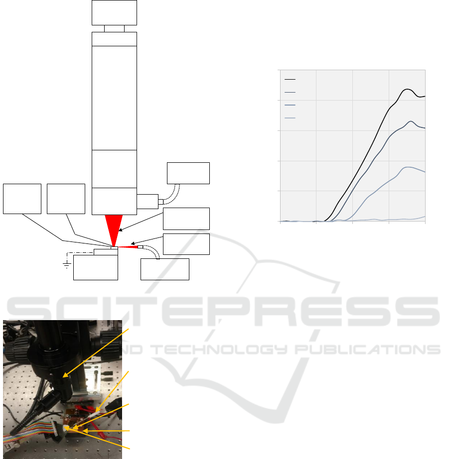
Figure 7: Schematic diagram of the SWIR microscope setup
for observation of the 2D spontaneous emission profile.
Figure 8: Photograph of the experimental setup.
3.3 Experimental Results
General device characterization of the tapered MOPA
structure occurred as follows. All measurements
were performed continuous wave at a controlled
temperature of 15 C. The device output power was
measured as a function of the injected amplifier
current for four master oscillator (single-mode ridge
section) injection current levels ranging from 0 mA to
300 mA. As shown in Figure 9, a maximum output
power of ~400 mW is achieved at I
MO
= 300 mA and
I
PA
= 4000 mA. The power vs. current characteristics
clearly shows that the tapered amplifier section does
not lase without optical injection from the master
oscillator section. The roll/kink behavior observed
above 3000 mA is attributed to the onset of
multimode oscillation.
Figure 9: CW power vs. tapered amplifier injection current
measured at four master oscillator current values and at a
heatsink temperature T = 15 C.
Figure 10 depicts the measured CW optical
spectra for the case where the amplifier current is held
constant while the master oscillator injection level is
varied. Figure 10 confirms the absence of laser action
when the master oscillator is turned off. As the
master oscillator current is increased, two features are
observed. First, a clear lasing peak appears and red-
shifts with increasing IMO. This behavior is
attributed to self-heating in the master oscillator
section of the device. Second, a large amplified
spontaneous emission pedestal appears around the
lasing peak. This ASE pedestal occurs due to the
excessively high threshold current of the master
oscillator section, which lacks any real feedback from
the front, and only 30% feedback in the rear. It is
clear from this result that the high threshold of the
master oscillator section limits the overall efficiency
of the device.
TEC
Heat Sink
Ridge
Current
Injection
Taper
Current
Injection
Fine Focus
Adjustable
Zoom
IR
Microscope
Adapter
C-mount
Coupler
SWIR
Camera
Microscope
Lamp Fiber
Fiber to OSA
/ thermopile
Spontaneous
Emission
Stimulated
Emission
Probe card (I
PA
)
Current probe (I
MO
)
Tapered laser chip
TEC controlled heatsink
SWIR microscope
0
100
200
300
400
500
0 1000 2000 3000 4000
Output Power (mW)
I
PA
(mA)
I
MO
= 300 mA
I
MO
= 200 mA
I
MO
= 100 mA
I
MO
= 0 mA
PHOTOPTICS 2017 - 5th International Conference on Photonics, Optics and Laser Technology
118
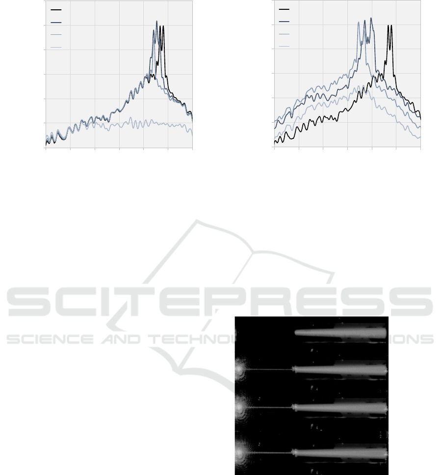
Figure 10: CW optical emission spectrum measured for a
constant power amplifier current of 4000 mA at four
different master oscillator current values at T = 15 C.
Figure 11 depicts the CW optical emission spectra for
the case where the master oscillator injection level is
held constant while the tapered amplifier current is
increased from 1000 mA to 4000 mA. The behavior
of this data series lends insight into the operation of
the tapered MOPA structure. At a current of 1000
mA, no lasing peak in the amplifier is observed – only
the spontaneous emission of the amplifier itself. This
is attributed to injection in the amplifier below the
transparency current density condition. As the
tapered amplifier current increases to 2000 mA, a
strong lasing peak at ~1500 nm is observed (two
longitudinal modes are evident). The background
spontaneous emission profile has also increased due
to the amplified spontaneous emission in the device.
As the current in the tapered amplifier is further
increased, the peak lasing wavelength and broadband
spontaneous emission profile are red-shifted (again
due to self-heating). Less obvious is an apparent
reduction in the total amplified spontaneous emission
due to increased gain saturation.
Figures 12 and 13 depict the SWIR microscope
images taken for the cases where the tapered
amplifier current is held constant and where the
master oscillator current is held constant,
respectively. The apparent blurring of the tapered
gain section is not caused by defocus; as previously
discussed the current injection is pixelated in this
region in order to create a lateral gain profile which
better matches the fundamental optical mode
amplified in this section. A significant amount of
light is seen to scatter off the rear facet of the power
amplifier and is caused by the etched trench which
serves to provide feedback to the master oscillator.
Figure 11: CW optical emission spectrum measured for a
constant master oscillator current of 300 mA at four
different power amplifier current values at T = 15C.
Scattering of the laser emission can also be seen
where the master oscillator and power amplifier
intersect and is caused by mode effective index
mismatch at this location. A small amount of laser
light can be seen scattering at the front facet of the
amplifier – this scattered light is attributed to
imperfections in the facet cleave or antireflection
coating.
Figure 12: SWIR microscope image of the spontaneous
emission measured at a constant tapered amplifier injection
current of 4000 mA and varying master oscillator injection
current values.
The simulation of this device predicted the low
output power of the single-mode master oscillator
section would make it difficult to observe the gain
saturation effects in the amplifier section. In the
analysis of the microscope images taken at I
PA
= 4000
mA, a nonlinear color map was applied
in order to investigate the gain saturation effects.
-90
-80
-70
-60
-50
-40
-30
1430 1450 1470 1490 1510 1530 1550
Relative Intensity (dB)
Wavelength (nm)
I
PA
= 4000 mA
I
MO
= 300 mA
I
MO
= 200 mA
I
MO
= 100 mA
I
MO
= 0 mA
-90
-80
-70
-60
-50
-40
-30
1430 1450 1470 1490 1510 1530 1550
Relative Intensity (dB)
Wavelength (nm)
I
MO
= 300 mA
I
PA
= 4000 mA
I
PA
= 3000 mA
I
PA
= 2000 mA
I
PA
= 1000 mA
I
MO
= 0 mA
I
PA
= 4000 mA
I
MO
= 100 mA
I
PA
= 4000 mA
I
MO
= 200 mA
I
PA
= 4000 mA
I
MO
= 300 mA
I
PA
= 4000 mA
Direct Observation of the 2D Gain Profile in High Power Tapered Semiconductor Optical Amplifiers
119
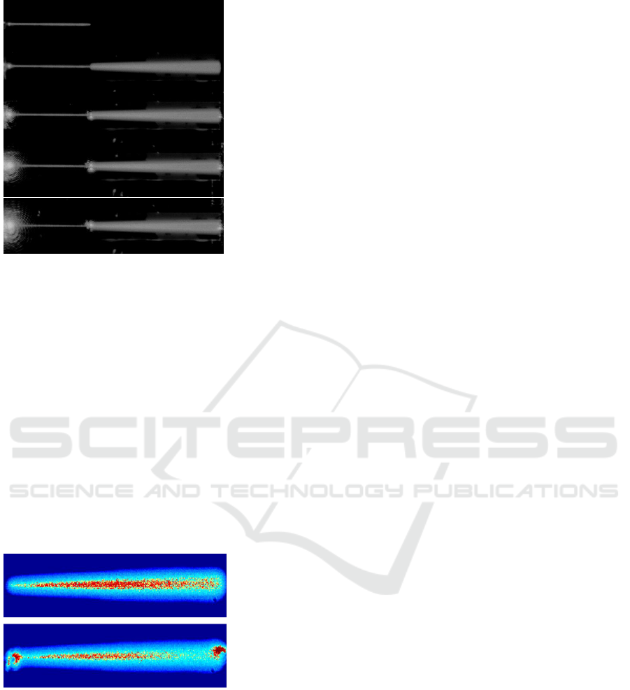
Figure 13: SWIR microscope image of the spontaneous
emission measured at a constant master oscillator injection
current of 300 mA and varying tapered amplifier injection
current values.
Figure 14 depicts the rescaled color map images of
the measured spontaneous emission profiles at I
MO
=
0 and 300 mA. As shown, there is a clear decrease in
the spontaneous emission, and hence gain, in the final
~35% of the device, just as predicted in the numerical
simulations. It is worth noting that the photon density
due to stimulated emission is many orders of
magnitude higher in this region at 300 mA than at 0
mA. Despite this, a reduction in the light captured by
the microscope in this region clearly indicates that the
optical signal being measured is spontaneous
emission from the quantum well (as opposed to
scattered stimulated emission).
Figure 14: Rescaled color map image comparing the
measured spontaneous emission profiles at zero and 300
mA master oscillator injection currents. Suppression of the
spontaneous emission near the exit of the facet of the
tapered amplifier is a clear indicator of gain reduction due
to local saturation.
4 DISCUSSION
The development of high power, high-efficiency
tapered amplifiers stands to benefit from
measurement techniques which enables a better
understanding of the internal device physics. This
work, for the first time, enables direct observation of
and mapping of the gain saturation effect in a
semiconductor optical amplifier. The technique relies
on the incorporation of a window in the back-side of
the device so that the spontaneous emission profile
can be directly observed for devices bonded junction
down. This first demonstration utilized a separately
addressable tapered MOPA device exhibiting an
unusually high master oscillator threshold current
attributed to antireflection coatings applied to both
sides of the device. Nevertheless, the effects of gain
saturation are clearly observed in the images taken.
Subsequent work in this area will first focus on
applying the technique to devices which operate at
much greater output levels. It is expected that this
technique will then be used to improve the gain
pixelation design to ensure more uniform gain
extraction over the entire area of the device.
ACKNOWLEDGEMENTS
The authors acknowledge support by NASA under
award number NNX16AD20G.
REFERENCES
J. P. Donnelly, J. N. Walpole, S. H. Groves, R. J. Bailey, et
al., "1.5-um tapered-gain-region lasers with high-CW
output powers," IEEE Photonics Technology Letters,
vol. 10, pp. 1377-1379, 1998.
S. R. Selmic, G. A. Evans, T. M. Chou, J. B. Kirk, et al.,
"Single frequency 1550-nm AlGaInAs-InP tapered
high-power laser with a distributed Bragg reflector,"
IEEE Photonics Technology Letters, vol. 14, pp. 890-
892, 2002.
T. Hao, J. Song, and P. O. Leisher, "Rate equation analysis
of longitudinal spatial hole burning in high-power
semiconductor lasers," Proc. of SPIE, pp. 91340S-
91340S-7, 2014.
T. Hao, J. Song, R. Liptak, and P. O. Leisher,
"Experimental verification of longitudinal spatial hole
burning in high-power diode lasers," Proc. SPIE. pp.
90810U-90810U-9, 2014.
S. L. Chuang, Physics of optoelectronic devices. New York:
Wiley, 1995.
P. Salet, F. Gerard, T. Fillion, A. Pinquier, et al., "1.1-W
continuous-wave 1480-nm semiconductor lasers with
I
MO
= 300 mA
I
PA
= 0 mA
I
MO
= 300 mA
I
PA
= 1000 mA
I
MO
= 300 mA
I
PA
= 2000 mA
I
MO
= 300 mA
I
PA
= 3000 mA
I
MO
= 300 mA
I
PA
= 3000 mA
I
MO
= 0 mA
I
PA
= 4000 mA
I
MO
= 300 mA
I
PA
= 4000 mA
PHOTOPTICS 2017 - 5th International Conference on Photonics, Optics and Laser Technology
120

distributed electrodes for mode shaping," IEEE
Photonics Technology Letters, vol. 10, pp. 1706-1708,
1998.
J. N. Walpole, J. P. Donnelly, L. J. Missaggia, Z. L. Liau,
et al., "Gaussian patterned contacts for improved beam
stability of 1.55-um tapered lasers," Photonics
Technology Letters, IEEE, vol. 12, pp. 257-259, 2000.
Direct Observation of the 2D Gain Profile in High Power Tapered Semiconductor Optical Amplifiers
121
