
Optimization of Transfer Times in Pinned Photodiodes
Lutz Girgenrath
1,3
, Martin Hofmann
1
, Ralf K
¨
uhnhold
1
and Holger Vogt
2,3
1
ELMOS Semiconductor AG, Heinrich-Hertz-Str. 1, 44227 Dortmund, Germany
2
Fraunhofer Institute for Microelectronic Circuits and Systems, Finkenstrasse 61, 47057 Duisburg, Germany
3
University Duisburg-Essen, Duisburg, Germany
Keywords:
CMOS Imaging, Lateral Drift-field Photodetectors (LDPD), High-speed Imaging, Large Pixels.
Abstract:
An implantation scheme which enhances the readout speed of a silicon pinned photodiode (PPD) with large
pixel length is presented. The basic PPD structure was developed for Time-of-Flight (TOF) distance measure-
ment applications by the Fraunhofer IMS in Duisburg, Germany, and was fabricated in a standard 0.35 µm
CMOS process. The optimized design of this PPD introduces the possibility to improve the electron readout
speed by changing the n-well configuration with a second well implantation. The local increase in doping
concentration creates a designated electron path which utilizes the reset voltage of the readout node. This
behaviour is shown by simulation and measurement results are presented.
1 INTRODUCTION
In recent years, the usage of optical and contact-
less distance measurements like phase-modulation or
time-of-flight has increased. These types of measure-
ments require high speed and high performance sen-
sors which are already widely used in entertainment
systems. In the last years they found their way into
the automotive sector for distance measurements and
gesture control. Since these systems require informa-
tion about the light pulse or phase, an external light
source is needed to illuminate the area. The usage
of IR-light is mandatory for scanning applications in
terms of eye safety and distraction. However, the
quantum efficiency (QE) of silicon for this part of the
spectrum is rather poor ((Green and Keevers, 1995))
and the sensors reach their limits when an applica-
tion needs both a high sensitivity and a fast signal ac-
quisition. Since the sensitivity is defined mainly by
the photosensitive area, one must use large diodes es-
pecially when operated in unfavourable environments
or with IR-light. However, increasing the sensor area
leads to a longer transfer time due to the quadratic
dependence between the length of the electron path
and the transfer time. Many groups tried to mitigate
this behaviour for smaller PPD ((Xu and Theuwis-
sen, 2013), (Tubert et al., 2009), (Han, 2015)). The
goal of this work is to maximize the diode length
while maintaining a sufficent transfer speed for 3D-
ToF measurements ((Driewer et al., 2016)) The ba-
Figure 1: a) Schematic design of the basic diode structure
invented by the Fraunhofer IMS in Duisburg and b) top view
of the readout and draining path.
sic diode structure which was used in this paper was
taken from the work of D. Durini, A. Spickermann
and A. Suess ((Durini et al., 2010), (Spickermann
et al., 2011), (S
¨
uss et al., 2013)). In this already en-
hanced pixel (fig. 1a) the n-well is directly connected
to the Floating Diffusion (FD) and the charge is not
any longer stored in the well but is accumulated in the
FD. The changed accumulation principle is crucial for
the presented type of n-well enhancement. Beside the
Transfer Gate (TG), there is a second gate for electron
accumulation called the Collection Gate (CG), which
is set to a constant positive potential. Furthermore a
second draining path was implemented (see fig. 1b) to
keep the n-well depleted between two accumulation
cycles. The electron current can be switched between
the signal (FD) and the draining path (DD). The diode
also features a lateral doping gradient which provides
312
Girgenrath L., Hofmann M., KÃijhnhold R. and Vogt H.
Optimization of Transfer Times in Pinned Photodiodes.
DOI: 10.5220/0006239603120316
In Proceedings of the 5th International Conference on Photonics, Optics and Laser Technology (PHOTOPTICS 2017), pages 312-316
ISBN: 978-989-758-223-3
Copyright
c
2017 by SCITEPRESS – Science and Technology Publications, Lda. All rights reserved

a built-in electrical field and the connection of the n-
well to the FD gives the opportunity to use the reset
voltage to implement a stronger electric field to the
diode as will be shown.
2 SIMULATION
The potential inside the n-well is pinned to a con-
stant value determined by the p+ top layer and the
p substrate and it depends on the doping concentra-
tions. Therefore, the dominating transport mecha-
nism is diffusion which is up to two orders of mag-
nitude slower than the electron transport in an electric
field. The pinned photodiode can be interpreted as a
simple p-n-p structure and the pinning voltge can be
calculated from the built-in potentials of the two p-n-
junctions. Thus the pinning voltage depends only on
the technology parameters, which are defined by the
implantation dose and implantation energy. There-
fore, the lateral doping gradient changes the pinning
voltage across the length of the diode and provides
a built-in electrical field. Since a gradient depends
on the length it is applied on, this effect vanishes in
bigger sensors. All previous mentioned solutions cre-
ate an internal field and are not implementable for
larger sensors (>15 µm). The key to increase the read-
out speed for large pixels is to introduce a potential
difference across the diode bigger than the pinning
voltage, which is only possible by bypassing the pin-
ning behaviour. We succeeded to achieve this with a
second well implantation to create a designated elec-
tron path with a slightly higher doping concentration.
The voltage distribution inside the n-well with and
without the second implantation is shown in figure
2. The readout voltage is not anymore suppressed by
the pinning behaviour. Also the depletion zone is ex-
panded. The implantation is applied at the end of the
front end of line so the thermal diffusion is negligi-
ble and the doping concentration increases only in a
distinct area of the well as an overall higher doping
concentration would reduce the width of the deple-
tion zone. However, the transition from the slightly
higher doping concentration of the n-well to the dop-
ing concentration of the readout node could result in
a barrier which slows down the electrons. Figure 3
shows the simulated conduction band energy across
the diode for different n-well implantation doses. The
barrier-free electron transport requires the conduction
band energy to follow a monotonic decreasing func-
tion. Figure 4 shows the maximum energy gradi-
ent under the CG as well as the maximum voltage
drop across the diode for the different implantation
doses. Without the second implantation the voltage
Figure 2: Simulation result of the voltage distribution across
the photodiode without the second implantation (top) and
with the second implantation (bottom). The electrons travel
through the diode on the path from B to A.
drop does not exceed 1 V. The simulations suggest to
set the target implantation dose to 3.0e11 cm
−2
. The
increased depletion region increases the quantum ef-
ficiency in the IR spectrum but decreases the well ca-
pacitance. The pixel performance is not affected by
the smaller capacitance as the electrons are stored in
the FD. Furthermore, a higher doping concentration
reduces the electron drift velocity ((Jacoboni et al.,
1977)) in a constant electrical field provided by the
pinning voltage. The decrease in mobility is compen-
sated by the 1.7 times stronger voltage gradient which
leads to an increased electron speed. Particularly the
strong electric field on the well interfaces drives the
electrons towards the readout node and the electron
velocity at these interfaces with the second implan-
tation is nearly two orders of magnitude higher. The
path-time-diagram for one electron based on the ve-
locity calculation (in figure 5) shows that the second
implantation can enhance the transfer time of the pho-
todiode doesn’t show a strong quadratic dependence
anymore. The influence of the strong field at the well
interface can be seen as the curve saturates. However,
these are the calculations for one electron and the time
to ensure complete charge transfer may be a factor of
5-10x longer in any PPD ((Fossum and Hondongwa,
2014)) especially if a barrier is present. It is important
for 3D-ToF measurements to reduce the transfer time
to a minimum as any remaining charge affects the dis-
tance calculation and thus reducing the measurement
range. A complete charge transfer after 10 ns is de-
sirable. Therefore, a diode length of 26 µm with the
second implantation could provide good results.
3 MEASUREMENT
We analyzed five different pixel configurations which
differ from each other by their length and implanta-
tion scheme. Table 1 shows the main differences be-
tween the measured devices. We extended the length
of the diode for the second device in order to see the
influence as the transfer time rises. The velocity simu-
lations are based on the implantation scheme of pixel
C. The higher doping concentration of 3.8e11 cm
−2
Optimization of Transfer Times in Pinned Photodiodes
313
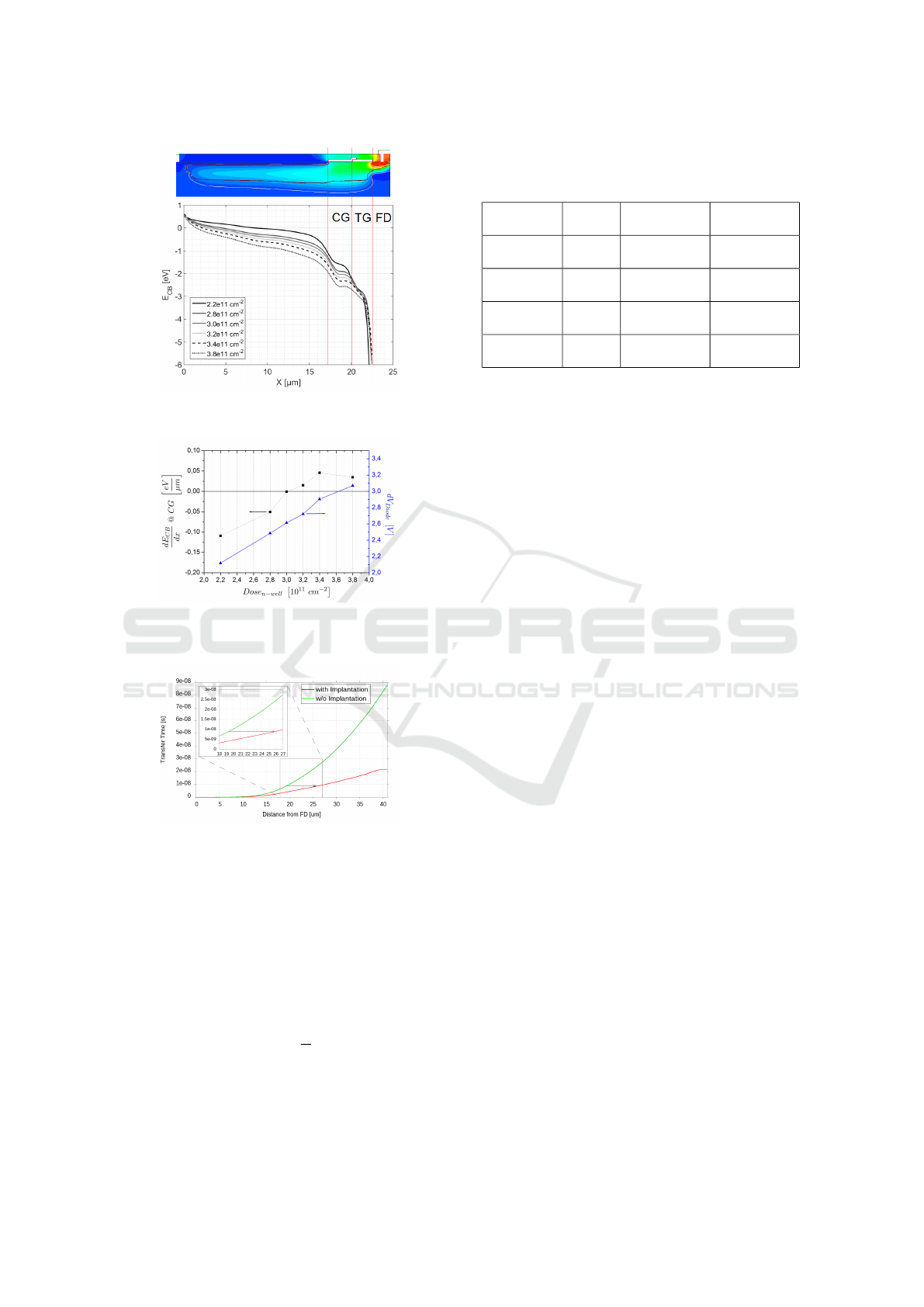
Figure 3: Simulation result of the conduction band energie
across the diode for different implantation doses.
Figure 4: Simulation of the maximum energy gradient un-
der the CG (left, black square) and the maximal voltage
drop across the diode (right, blue triangle).
Figure 5: Path-time-diagram for one electron of a simulated
40 µm photodiode along the path from A to B.
for the short reference pixel derive from the optimiza-
tion of the charge storage. The schematic measure-
ment setup is shown in figure 6. The chip is positioned
in-plane with the laser and is illuminated indirectly
over two mirrors which redirect the light beam of the
laser towards the camera. The mirrors are attached to
a moving platform to adjust the distance between the
laser and the sensor. We used different distances to
change the light itensity on the sensor as the radiation
angle of the laser is 10
◦
(I ∝
1
r
2
). The highest possi-
ble intensity with a propagation distance of 200 mm
is defined as I
0
. We measured laser response curves
which not only give information about the shutter ef-
ficiency but also about the transfer behaviour of the
Table 1: Length and implantation scheme of the measured
pixel configurations.
Pixel Length n-well Impl. 2nd Impl.
A
Ref. Short
19 µm
Phosphorus
3.8e11 cm
−2
-
B
Ref. Low
26 µm
Phosphorus
3.0e11 cm
−2
-
C
Impl. Low
26 µm
Phosphorus
3.0e11 cm
−2
Phosphorus
1.0e11 cm
−2
D
Ref. High
26 µm
Phosphorus
3.8e11 cm
−2
-
E
Impl. High
26 µm
Phosphorus
3.8e11 cm
−2
Phosphorus
1.0e11 cm
−2
electrons. Figure 7 shows the measurement princi-
ple to extract the laser response curves. The trigger-
ing of the laser and the shutters is performed on-chip
and the positions of the pulses refer to this global trig-
ger. The laser pulse is shifted towards the TG1 shutter
which is positioned at 75 ns. The laser delay can be
adjusted in time steps of 6.25 ns. The laser response is
then plotted against the time remaining between TG1
shutter and laser pulse (time before shutter: t
BFS
) as
a function of the propagation delay in respect to the
time of flight of the laser pulse. An ideal photodiode
with infinite electron speed should not show any sig-
nal before the laser and the TG1 shutter overlap. This
means that the time the first signal is recorded is equal
to the transfer time for a complete charge transfer. All
measurements take place in the dark. The background
signal of the sensor which is subtracted from the sig-
nal is also measured. The TG1 shutter length t
S
is
set to the lowest value so only electrons with a trans-
fer time between t
BFS
and t
BFS
+ t
S
will contribute to
the signal output. The number of accumulation cycles
was adjusted to just reach the maximum output for the
highest signal level to maintain comparability of the
devices and the different t
BFS
. Therefore, the num-
ber of accumulation cycles represent the sensitivity of
the sensor. Since the relation between the light inten-
sity and generated electrons is linear, the number of
accumulations to fill the readout capacitance should
be proportional to the light intensity. We analyze the
pixel performance by their charge transfer efficiency.
Since the diode is always connected to one of the two
draining paths, the charge transfer inefficiency (CTI)
is given by the amount of generated electrons which
are not effectively drained from the n-well before the
TG1 shutter opens and therefore contributing to the
FD discharge. The CTI is equal to the voltage drop
if the signal reaches the maximum possible output as
the accumulations are set to a constant value. For
lower signal levels the CTI is calculated in respect
to the highest measured signal. An ideal diode with
infinite electron speed should show the first signal af-
PHOTOPTICS 2017 - 5th International Conference on Photonics, Optics and Laser Technology
314
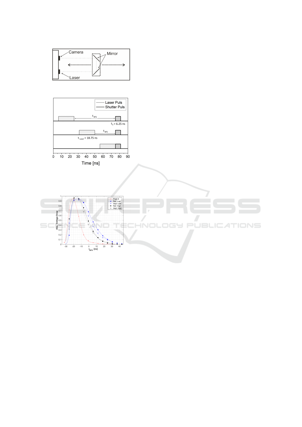
Figure 6: Measurement setup to extract the laser response
curves.
Figure 7: Measurement principle to extract the laser re-
sponse curves. The signal level is plotted against the time
remaining between laser and shutter. The positions refer to
the global on-chip trigger.
Figure 8: Normalized laser response curves of the five dif-
ferent pixel configurations for I = I
0
.
ter the laser and TG-shutter overlaps with no CTI at
0 ns. The corresponding laser response curve of an
ideal sensor gives the exact form of the laser pulse. A
slower readout speed shifts the peak towards longer
transfer times and broadens the measured pulse as the
electrons are not drained fast enough from the diode.
Therefore, the CTI at 0 ns gives a good idea of the
quality of the measured pulse.
4 RESULTS
The measurement results of the different pixel vari-
ations are presented in figure 8. The absolute volt-
age drop is calculated relative to the maximum sig-
nal level of the sensor. The increase in diode length
from 19 µm (Pixel A) to 26 µm (Ref. High) increases,
as expected, the transfer time as well. Directly af-
ter the laser puls, 8 % of the charges remain in Pixel
A. So the curve represents the laser pulse reasonably
well while in the longer version of this pixel (Ref.
High) 49 % of the charges remain at 0 ns and the time
to reach the same CTI as the short version is up to
20 ns longer. The simulation (fig. 5) shows transfer
times of 9 ns for 19 µm and 25 ns for 26 µm which
are in good agreement with the measured laser re-
sponse curves. Reducing only the doping concentra-
tion of the n-well results in a stronger influence of the
pinning voltage which slows down the readout speed
significantly. Therefore, the second implantation en-
hances the transfer behaviour but not as noticeable as
suggested by the simulation. The measurements for
lower intensities (fig. 9a and 9b) show an increase
in CTI for pixels with a higher n-well doping con-
centration while the CTI for pixels with lower n-well
doping concentration remain stable. As discussed in
chapter 2, the increased doping concentration affects
the well capacitance and the depletion zone. Also a
barrier is formed in the readout path. This effect is
observable in the number of accumulation cycles to
reach the maximum voltage drop (fig. 10). The rela-
tion between the intensity and the number of cycles
is not linear for the higher doping concentration. The
number of electrons which are generated by incident
photons is affected by the depletion zone. As long
as there are enough electrons the barrier is not ob-
served in the number of accumulations. Therefore,
the influence of the barrier vanishes for higher inten-
sities which provide enough electrons to fill the FD.
The second implantation enhances the performance of
the pixel but the mismatch between measurement and
simulation suggests a barrier in the readout path even
for the reduced n-well implantation dose. The barrier
is probably formed by bulk effects which are not cov-
ered by a 2D simulation. A further enhancement in
transfer speed should still be achievable by adjusting
the well configuration under the CG.
5 CONCLUSIONS
In this work a new type of n-well enhancement for a
pinned photodiode was presented. It has been shown
that a local increase in doping concentration of the
n-well enhances the transfer speed of a specific type
of pinned photodiode. The simulation shows that a
26 µm long photodiode reaches the same performance
in terms of transfer speed as a 19 µm long photodiode.
Therefore, it is possible to mitigate the quadratic de-
pendence of the transfer time from the diode length.
Optimization of Transfer Times in Pinned Photodiodes
315
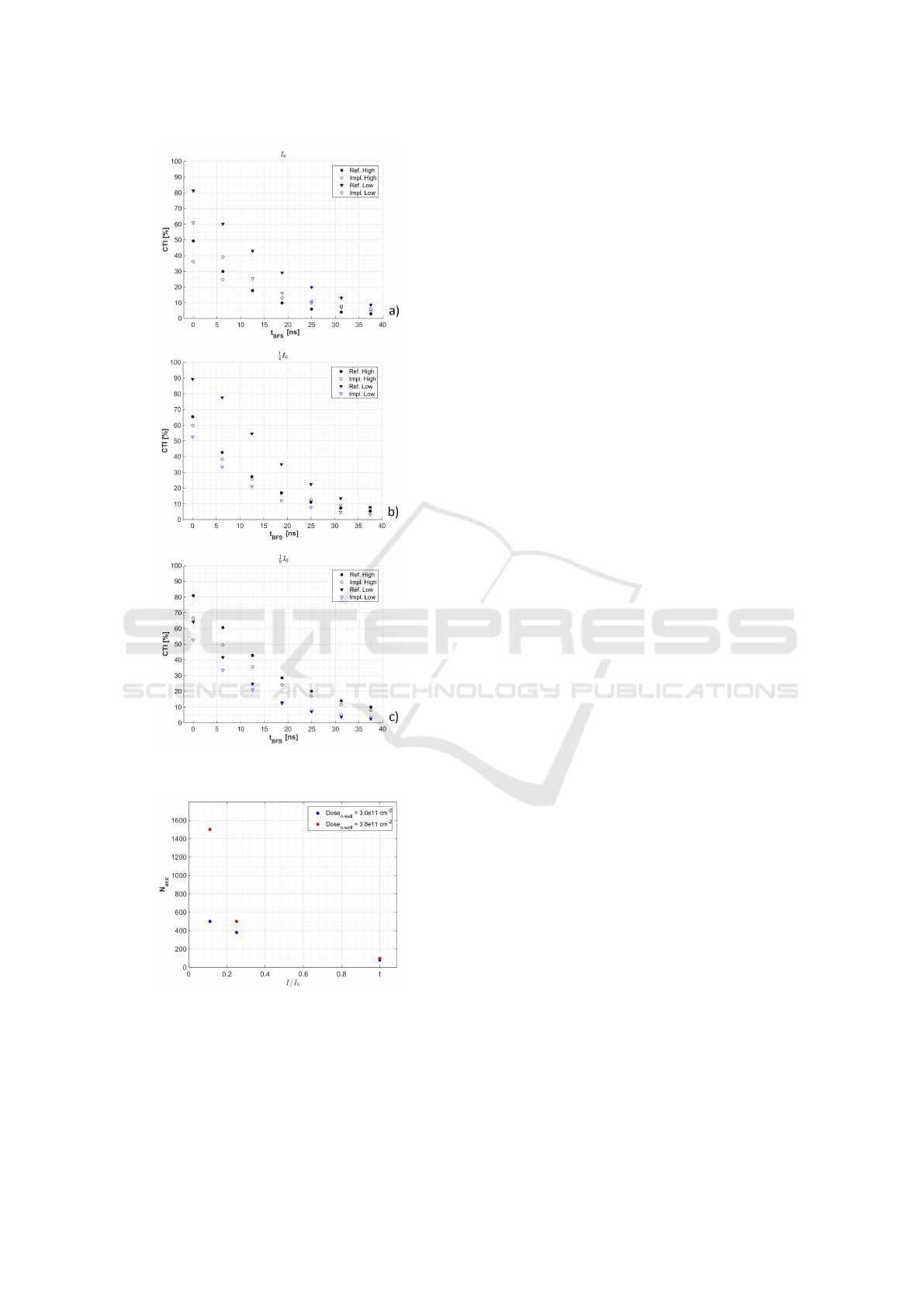
Figure 9: CTI measurements for the longer pixel in relation
to the light intensity. a) I = I
0
b) I = 0.25I
0
c) I = 0.11I
0
.
Figure 10: Number of accumulation cycles which are ness-
esary to reach the maximum voltage drop for different light
intensities.
Nevertheless, without prior optimization of the con-
nection of the readout path and the n-well, the transfer
behaviour of a 26 µm long PPD was only slightly im-
proved. The readout speed of the full n-well (t
BFS
= 0)
was increased by up to 40 % for the same pixel length.
For longer transfer times no significant improvement
could be achieved due to possible formation of a bar-
rier. However, stable results over a wide intesity range
can be achieved if the n-well doping concentration is
adjusted in respect to the second implantation. The n-
well configuration at the transition between well and
readout path remains crucial in terms of transfer speed
and will be investigated in the future.
REFERENCES
Driewer, A., Hosticka, B. J., Spickermann, A., and Vogt,
H. (2016). Modeling of the charge transfer in a lat-
eral drift field photo detector. Solid State Electron.,
126:51–58.
Durini, D., Spickermann, A., Mahdi, R., Brockherde, W.,
Vogt, H., Grabmaier, A., and Hosticka, B. J. (2010).
Lateral drift-field photodiode for low noise, high-
speed, large photoactive-area cmos imaging applica-
tions. Nuclear Instruments and Methods in Physics
Research Section A: Accelerators, Spectrometers, De-
tectors and Associated Equipment, 624:470–475.
Fossum, E. R. and Hondongwa, D. B. (2014). A review of
the pinned photodiode for ccd and cmos image sen-
sors. IEEE J-EDS, 2:33–43.
Green, M. and Keevers, M. (1995). Optical properties of
intrinsic silicon at 300 k. Progress in Photovoltaics:
Research and Applications, 3:189–192.
Han (2015). A time-of-flight range image sensor with back-
ground canceling lock-in pixels based on lateral elec-
tric field charge modulation. IEEE J-EDS, 3:639–641.
Jacoboni, C., Canali, C., Ottaviani, G., and Quaranta, A. A.
(1977). A review of some charge transport properties
of silicon. Solid State Electron., 20:77–89.
Spickermann, A., Durini, D., S
¨
uss, A., Ulfig, W., Brock-
herde, W., Hosticka, B. J., Schwope, S., and Grab-
maier, A. (2011). Cmos 3d image sensor based on
pulse modulated time-of-flight principle and intrinsic
lateral drift-field photodiode pixels. ESSCIRC, 2011
Proceedings of the, pages 111–114.
S
¨
uss, A., Nitta, C., Spickermann, A., Durini, D., Varga,
G., Jung, M., Brockherde, W., Hosticka, B. J., Vogt,
H., and Schwope, S. (2013). Speed considerations
for ldpd based time-of-flight cmos 3d image sensors.
European Solid State Circuits Conference (ESSCIRC),
pages 299–302.
Tubert, C., Simony, L., Roy, F., Tournier, A., Pinzelli, L.,
and Magnan, P. (2009). High speed dual port pinned-
photodiode for time of flight. Proc IISW.
Xu, Y. and Theuwissen, A. J. (2013). Image lag analysis
and photodiode shape optimization of 4t cmos pixels.
IISW, 153.
PHOTOPTICS 2017 - 5th International Conference on Photonics, Optics and Laser Technology
316
