
Simulation of Copper Thin Film Thickness Optimization for Surface
Plasmon using the Finite Element Method
Tanaporn Leelawattananon
1
, Kitsakorn Locharoenrat
1
and Suphamit Chittayasothorn
2
1
Department of Physics, Faculty of Science, King Mongkut’s Institute of Technology Ladkrabang, Thailand
2
Department of Computer Engineering, Faculty of Engineering, King Mongkut’s Institute of Technology Ladkrabang,
Bangkok, Thailand
Keywords: Surface Plasmon Wave, Kretschmann Configuration, Finite Element Method, Simulation.
Abstract: This paper presents a computer simulation of optical activations based on the Kretschmann configuration
using a prism for the observation of the surface plasmon wave. This is according to the condition of the
dispersion relation. The analysis of the electric field of the surface plasmon wave which appears at the
interface between the metal layer and the air layer is done by using the Finite Element Method (FEM). The
simulation is performed using the COMSOL Multiphysics software which supports the FEM. The objective
of our experiment is to find the most suitable thickness of the metal thin film which is most suitable for the
surface plasmon excitation when activated by 632.5 nm red laser light source. The red laser light source is
commonly available and also very economical. The metal used in our work is copper which is an
economical noble metal and gives better conductivity than gold. The findings from the simulation will be
used in the future high precision physical experiments. The outcome of this research project, the surface
plasmon wave on copper thin film, is expected to be used in bio-molecular detectors or high speed THz
communications.
1 INTRODUCTION
During the past decades, the need to verify and
process data by using optics have been growing and
developing rapidly. Optical sensors which are able
to detect bio-molecular objects such as DNA protein
are widely available. They have both sensitivity and
size advantages over non-optical sensors (Anker et
al., 2008). These optical sensors use the Surface
Plasmon Resonance (SPR) principle which works by
the optical excitation at the interface between the
metal thin film layer and dielectric layer (or the test
sample layer). The most widely used noble metals
for the metal layer is gold. Gold has less oxidation
and is very resistant to atmospheric contaminants
(G. Boisde, A. harmer, 1996). However, gold is very
expensive. It has been recently found that copper has
better conductivity than gold. It is also cheaper. The
main disadvantage of copper is the ease of having
oxidation. However, copper is better in term of
diffusion. Copper does not diffuse into the silicon
substrate when gold does. Copper is therefore used
in the standard silicon manufacturing process such
as CMOS technology (G.V. Naik, et al., 2013).
Furhermore, there is a research result which reports
that copper is an excellent plasmonic material (P.
Robusto, R. Braunstein, 1981). Also, according to a
research work (V.G. Kravets, et al., 2014), the
application of Graphene layer over copper layer can
significantly reduce the oxidation; thus the copper
layer is slowly deteriorated and improves plasmonic
characteristic.
Recently, surface plasmon wave find
applications in high speed communications and high
frequency electronic technology since they have
frequencies in the THz ranges (H. Sakai et al.,
2016).
The thickness of the metal film has direct effects
to the excitation of the surface plasmon wave, both
from the consistency of the waves and the
amplitudes of the electric fields of the waves. In
order to find the optimum waves for the given metal
and the given optical source, this project models the
excitation using the Kretschmann configuration. We
also analyze the result electric field of the surface
plasmon wave which take place at the interface
between the metal thin film layer and the sample test
layer using the finite element method (FEM). We
intend to use the economical 632.5 nm red laser light
source with thin film copper. The COMSOL
188
Leelawattananon, T., Lorchalearnrat, K. and Chittayasothorn, S.
Simulation of Copper Thin Film Thickness Optimization for Surface Plasmon using the Finite Element Method.
DOI: 10.5220/0006395601880195
In Proceedings of the 7th International Conference on Simulation and Modeling Methodologies, Technologies and Applications (SIMULTECH 2017), pages 188-195
ISBN: 978-989-758-265-3
Copyright © 2017 by SCITEPRESS – Science and Technology Publications, Lda. All rights reserved
Multiphysics software (COMSOL Inc., 2017) which
supports the FEM is employed.
2 THEORETICAL
BACKGROUNDS OF THE
SURFACE PLASMON
RESONANCE (SPR)
Surface plasmon waves or surface plasmon
polaritons (SPPs) are generated at the surface
between metal-dielectric interfaces when excited by
the incoming light with an appropriate frequency.
The excitation of surface plasmon waves can be
done by having light beams contact prisms and the
phase of the light at the metal-dielectric interface is
matched to the phase of the surface plasmon waves.
In the early years of the research in this area Otto
(Y. Suzuki et al., 1989) and Kretschmann (T.A.
Leskova et al., 2000) developed an experimental
optical excitation which created SPs waves by using
a prism and coated a metal thin film on the surface
of the prism. Attenuated total reflection (ATR) is a
technique to observe the plasmons. The reflected
light intensity are measured by changing the incident
angles of the incoming light to various degrees. At a
certain angle which is referred as the "resonance
angle", the reflected ATRs from the prism signifies
the light absorption by the electrons in the metal and
their resonance which in turn creates the surface
plasmon wave at the metal–dielectric interface.
Apart from this, there are also researches which use
the grating (A. Iadicicco et al., 2005) and optical
waveguides (Wei Du and Feng Zhao, 2014) for the
optical excitations of surface plasmons.
The Kretschmann method employs a detecting
microscope which moves to different positions to
give different angles as shown in Figure 1. When
the incoming light travels from the medium which
has higher refractive index to the medium which has
lesser refractive index, and the light impacts the
interface between the two medium with the angle
greater than the critical angle, the light will be
totally reflected. This phenomenon is called Total
Internal Reflection (TIR). The TIR creates a kind of
electromagnetic wave between the contact surfaces
of the two media called the evanescent
electromagnetic field. The minimum amount of the
total internal reflection is observed when the
incoming energy of the incident light is coupled onto
the flat metal. This is referred to as “attenuated total
reflection” (ATR).
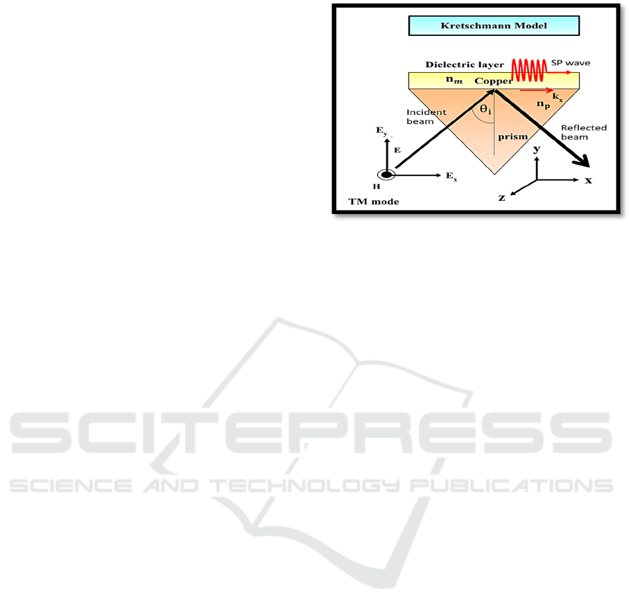
Figure 1: Surface Plasmon excitation at the surface when
activated by light impact to the prism using the
Kretschmann’s configuration.
As shown in Figure 1, the TM-polarized incident
light impacts the prism and activates the excitation
of the surface plasmon waves at the interface
between the metal thin film and dielectric layer (air
layer). The wave vector of the light can be adjusted
to be equal to the wave vector of the surface
plasmon by launching it from the prism through the
metal thin film. The prism is a medium with a higher
refractive index than the metal film. Light moving in
the prism is reflected at the prism-metal layer
interface by means of total internal reflection. The
evanescent field of the reflected light at the prism-
metal interface penetrates into the metal. With the
appropriate thickness of the metal layer, the
evanescent wave reaches the metal-dielectric
interface (or metal-air interface). In the case that the
phase of the incoming light propagating in the prism
matches the phase of the surface plasmon waves, the
surface plasmon resonance is generated and surface
plasmon waves propagate along this metal-dielectric
interface. They are generated according to a certain
condition which depends on the incident angle and
the incident wavelength:
k
k
k
n
sin
θ
(1)
k
sp
is the wave vector of surface plasmon waves
k
x
is the wave vector of the incoming light
n
p
is the refractive index of the prism
θ is the resonance angle ( ATR angle)
According to the equation, the energy and
momentum of the incoming light which impact the
prism are transfered to the electrons group of the
metal thus excites surface plasmon wave. Dispersion
relation of surface plasmon wave is shown in the
following equation:
Simulation of Copper Thin Film Thickness Optimization for Surface Plasmon using the Finite Element Method
189

k
k
ω
c
ε
ε
ε
ε
(2)
When the dispersion relation is combined with
the excited condition, it is found that the minimum
incident angle of the incoming light is:
θ
sin
1
n
ε
ε
ε
ε
(3)
If the wavelength of the incident light and the
relative permittivity of the metal layer are known,
the suitable incident angle which activates the
surface plasmon wave can be calculated.
3 THE SIMULATED
EXPERIMENTS
The excitation of the surface plasmon resonance
phenomenon needs to have the k-vector of the
activating light which impacts the prism equals to
the k-vector of the surface plasmon wave (SP wave)
at the interface between the metal thin film layer and
the air layer. We therefore simulate the light
activation using the Kretsckmann’s configuration
which is a relatively easy to implement activation
method. A prism with high refractive index and
coated with copper thin film is implemented as
shown in Figure 2. Electric fields of the surface
plasmon wave at the copper-air interface (metal-air
interface) are analyzed using the finite element
method (FEM). The COMSOL Multiphysics
software is deployed.
Parameters as shown in the Table 1 are set
according to the dispersion relation. This is to make
the k-vector of the p-polarized (TM mode) light
which impacts the prism equals to the k-vector of the
Figure 2: The optical excitation of the Kretschmann’s
configuration.
SP wave. When the light penetrates into the metal
thin film, free electrons groups in the metal are
coupling with the activating light and vibrate
resonantly with the frequency of light. This
phenomenon is called the surface plasmon resonance.
When the incident angle of the light is equal to
the resonance angle (also called the Attenuated Total
Reflection angle θ
ATR
), the parallel component of k-
vector of the incoming light is matched to the
parallel k-vector of the surface plasmon. At this
stage, the light transfers its energy to electrons
groups in the metal and becomes surface plasmon
energy. There is no reflect back of the light from the
prism. The evanescent wave at the metal-dielectric
layer couples to the surface plasmon which results in
the propagation of the surface plasmon wave along
to the metal-air interface as previously mentioned.
Table 1: Important parameters of each medium.
Parameter name Value
Refractive index of Air 1
Refractive index of Prism
(BK7)
1.5151
Relative permittivity of Prism
(Real part)
2.2955
Relative permittivity of Prism
(Imaginary part)
3.6715e-8
Refractive index of Copper
Thin film
0.30730
Relative permittivity of Copper
(Real part)
-11.681
Relative permittivity of Copper
(Imaginary part)
2.1090
Incident wavelength of Light 632.5 nm
Power of Light 1 W
kx
k0*n
prism
*sin(θ)
ky
k0*n
prism
*cos(θ)
In this simulation project, the incident angles are
changed gradually 1 degree at a time from 30 to 80
degrees. Corresponding surface resonance waves
which are activated by the light are observed. The
light source is the TM mode laser which has the
wavelength of 632.5 nm with a power of 1 W. The
simulated thickness of the copper layer varies from
20 nm, 40 nm, 60 nm, 80 nm to 100 nm.
Electromagnetic wave propagation as described
by the Maxwell’s wave equation (in frequency
domain) is as follows:
E
k
ε
E0
(4)
where
is the
relative permittivity of material
SIMULTECH 2017 - 7th International Conference on Simulation and Modeling Methodologies, Technologies and Applications
190
E is the
electric field equation
is the
wave vector in free space
It is a differential form equation. We use this
equation in the RF module of the Comsol
Multiphysics for analyzing the amount of the
electromagnetic field at the interface between the
thin metal film and the air.
Moreover, we specify Floquet boundary
condition both at the left surface and the right
surface of every layer in this model to ensure the
symmetry of the electric field along and parallel to
the interface in the x-y plane.
We also determine the Port boundary condition
of this model by using the
bottom boundary as
Active Port for light impact. The
input power of the
laser source is set to
1 Watt. The top boundary is
used as the Passive Port
which allow light to be
transmitted through without reflections.
For the meshing of the 2D geometry in this
research work, We partition
the subdomain into
triangular mesh elements. The resolution of the
mesh is set to be extra fine.
For the impact angle from 30 to 80 degrees, we
use the Parametric Sweep to be
range(alpha_min,alpha_step,alpha_max)
where
alpha_min
is equal to
30
degrees, alpha_max is
equal to
80 degrees, and alpha_step is 0.01 degrees.
After specifying physical quantities such as
material properties, constraints, parameter,
COMSOL Multiphysics is then
internally compiles
all related
PDE equations automatically using the
finite element analysis. Multiple solvers are used
together with adaptive meshing and error control
which has been previously specified. Results can be
observed from the graphical user interface.
4 RESULTS
In the first analysis using the finite element method
on the COMSOL Multiphysics software, the TM-
polarized incident light with the 632.5 nm
wavelength impacts the prism with different impact
angles. We found that when the surface plasmon
resonance phenomenon takes place at the interface
between the air layer and the copper layer with the
thickness of 20 nm, 40 nm, 60 nm, 80 nm, and 100
nm, there are surface plasmon waves when the
incident angle of the incoming light is 44.8 degrees.
The incident angle and the light’s wavelength
correspond with the dispersion relation equation.
However, the characteristics of the electric field of
surface plasmon wave are different when the
thickness of the thin copper film layer is changed.
When the surface plasmon resonance
phenomenon is taking place at the contact point
between the metal thin film and the air, if the
thickness of the metal film is suitable, and the
impact angle of the TM mode light is suitable, the
simulated electric field at the interface will be
clearly seen with high amplitude. This demonstrates
that the light reflectance
approaches the minimum or
even zero. Such an angle is called the
resonance
angle.
The resonance angel can be shifted if the
dielectric layer is changed to other materials such as
biomolegular sustances. The resonance angle is
therefore can be applied to checked the existence of
bio-molecular DNA.
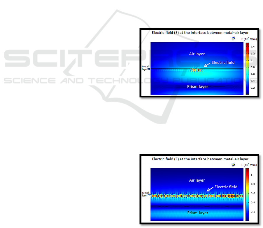
When the copper thin film thickness is 20 nm, it
is found that the electric field between the interface
of the copper film and the air has low amplitudes.
The average amplitude is 5.1x10
4
V/m as shown in
Figure 3. The electric field that occurs does not
show clear patterns and does not seem to be
consistent along the copper-air interface.
Figure 3: Electric fields of surface plasmon wave at the
interface between the 20 nm copper film and the air.
When the copper thin film thickness is 40 nm, it
is found that the electric field between the copper-air
interface has high amplitudes. The average
amplitude is 2.7x10
5
V/m as shown in Figure 4. The
Figure 4: Electric fields of surface plasmon wave at the
interface between the 40 nm copper film and the air.
Simulation of Copper Thin Film Thickness Optimization for Surface Plasmon using the Finite Element Method
191
electric field that occurs show clearer patterns and
consistent along the copper-air interface.
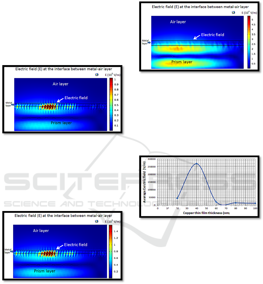
When the copper thin film thickness is 60 nm, it
is found that the electric field between the interface
of the copper film and the air has low amplitudes.
The average amplitude is 2.2x10
4
V/m as shown in
Figure 5. The electric field that occurs show unclear
patterns and not consistent along the copper-air
interface.
Figure 5: Electric fields of surface plasmon wave at the
interface between the 60 nm copper film and the air.
When the copper thin film thickness is 80 nm, it
is found that the electric field between the interface
of the copper film and the air has low amplitudes.
The average amplitude is 2.9x10
4
V/m as shown in
Figure 6. The electric field that occurs show unclear
patterns and not consistent along the copper-air
interface.
Figure 6: Electric fields of surface plasmon wave at the
interface between the 80 nm copper film and the air.
When the copper thin film thickness is 100 nm, it
is found that the electric field between the interface
of the copper film and the air still has very low
amplitudes. The average amplitude is 1.1x10
4
V/m
as shown in Figure 7. However, the electric field that
occurs does not show clear patterns and is not
consistent along the copper-air interface. The
patterns can not be used to identify if they are
surface plasmon wave at the interface.
Figure 7: Electric fields of surface plasmon wave at the
interface between the 100 nm copper film and the air.
A graph is plotted to show the relationship
between the maximum amplitude of the electric field
at the copper-air interface and the thickness of the
copper film. The graph shows a concave downward
pattern. The highest point of the graph is when the
thickness of the copper film is 40 nm. This is the
best point when activated by the 632.5 nm light
source.
Figure 8: The graph which shows relationships between
the maximum amplitude of the electric field at the copper-
air interface and the thickness of the copper thin film.
The next step is to find the most suitable impact
angle for the given light source. We then change the
impact angle parameter to other values around the
44.80 degrees (this is the degree according to the
dispersion relation equation) and keep the impact
light TM mode to have the wavelength of 632.5 nm
to find a suitable impact angle for best surface
plasmon resonance phenomenon. The simulated
observable surface plasmon wave with highest
amplitude at the interface between the copper thin
film and the air are considered. Table 2 shows the
observation results.
After having the first results, the second analysis
is conducted. The finite element method on the
COMSOL Multiphysics software is still employed.
The wavelength of the TM-polarized incident light is
changed to be 785 nm with a power of 1 W and the
SIMULTECH 2017 - 7th International Conference on Simulation and Modeling Methodologies, Technologies and Applications
192
incident angle is now changed to be 44 degrees. The
thickness of the thin copper film are 20 nm, 40 nm,
60 nm, and 80 nm. The simulated electric field
patterns and amplitudes are observed.
Table 2: The incident angles (ϴ
ATR
) which are suitable for
different copper thin film thickness.
Copper
thin film
thickness
(nm)
Optimized
incident
angle
(ϴ
ATR
,
degrees)
Δϴ
(degrees)
E
avg
(V/m)
20 44.14 0.66 4.4x10
4
40 44.80 0 2.7x10
5
60 44.84 0.04 2.1x10
4
80 44.86 0.06 1.4x10
4
100 45.88 1.08 1.2x10
5
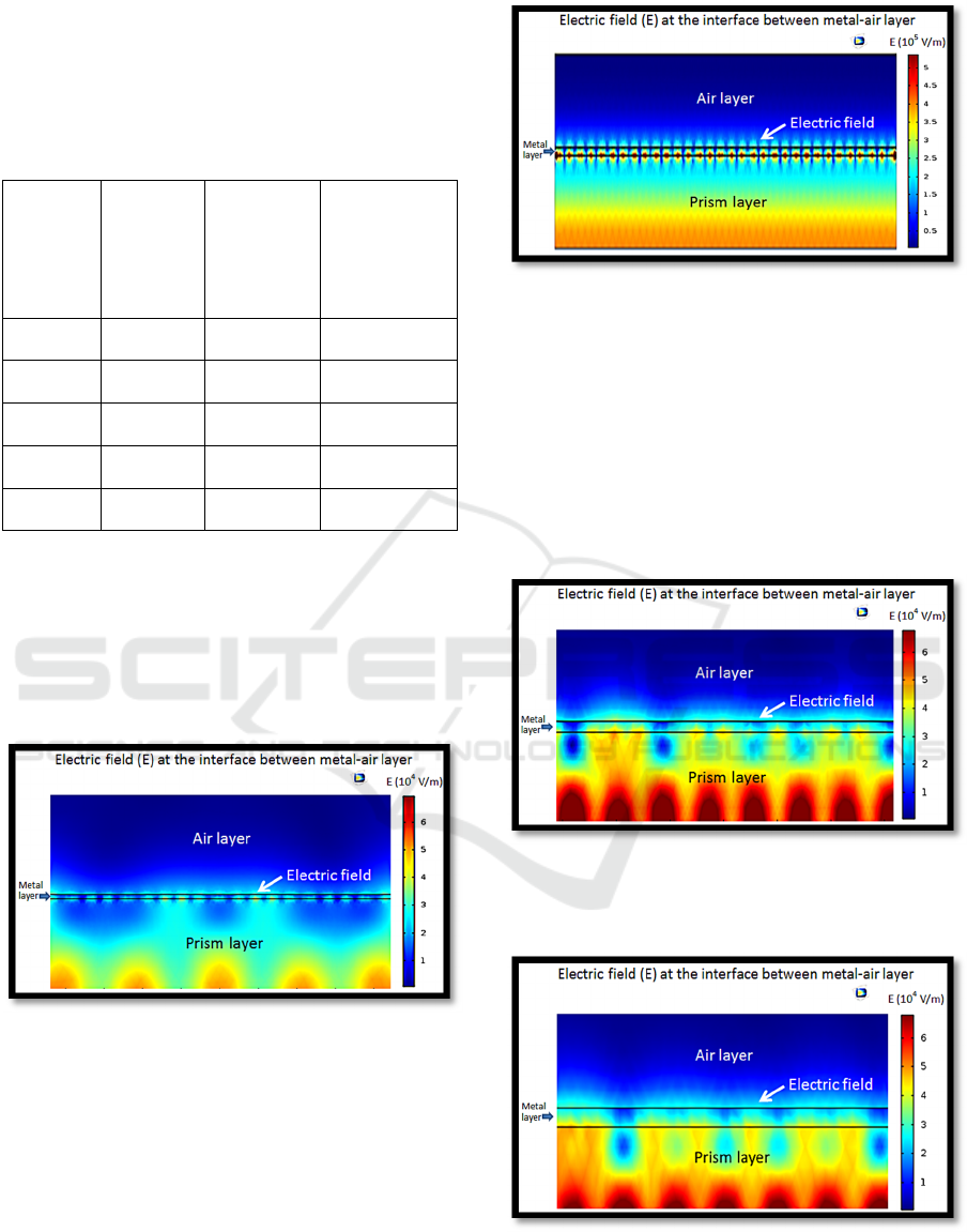
When the copper thin film thickness is 20 nm, it
is found that the electric field between the interface
of the copper film and the air has low amplitudes.
The average amplitude is 2.8.x10
4
V/m as shown in
Figure 9. The electric field that occurs show clear
patterns and consistent along the copper-air
interface.
Figure 9: Electric fields at the interface between the 20 nm
copper film and the air when the light has 785 nm
wavelength.
When the copper thin film thickness is 40 nm, it
is found that the electric field between the interface
of the copper film and the air has high amplitudes.
The average amplitude is 2.5x10
5
V/m as shown in
Figure 10. The electric field that occurs show clear
patterns and consistent along the copper-air
interface.
Figure 10: Electric fields at the interface between the 40
nm copper film and the air when the light has 785 nm
wavelength.
When the copper thin film thickness is 60 nm, it
is found that the electric field between the interface
of the copper film and the air has low amplitudes.
The average amplitude is 2.5x10
4
V/m as shown in
Figure 11. The electric field that occurs show
unclear patterns and not consistent along the copper-
air interface.
Figure 11: Electric fields at the interface between the 60
nm copper film and the air when the light has 785 nm
wavelength.
Figure 12: Electric fields at the interface between the 80
nm copper film and the air when the light has 785 nm
wavelength.
Simulation of Copper Thin Film Thickness Optimization for Surface Plasmon using the Finite Element Method
193

When the copper thin film thickness is 80 nm, it
is found that the electric field between the interface
of the copper film and the air has low amplitudes.
The maximum amplitude is 2.7x10
4
V/m as shown
in Figure 12. The electric field that occurs show
unclear patterns and not consistent along the copper-
air interface.
From the simulation results, it is found that the
thickness of the thin copper film has direct effect to
the occurrence of the surface plasmon waves. The
thickness of 40 nm is considered the best thickness
for the activation with the 632.5 nm wavelength. It
yields very clear and consistent surface plasmon
waves pattern. It also has the highest electric field
amplitude at the copper-air interface.
Our analysis results which are obtained by using
the finite element method, give similar results to (F.
Atida Said et al., 2016) which uses the finite
difference method when the incident light source has
785 nm wavelength. That is, when the light source
with the 785 nm wavelength is used, the best copper
thin film thickness is 40 nm. It gives high and
consistent surface plasmon wave amplitudes at the
copper-air interface.
5 CONCLUSIONS
Recently, researches in the area of plasmonics have
been highly active. There are applications in various
areas such as biomedical engineering where SPR
devices are used as sensors to detect the presence of
DNA molecules which are adhered to metal
surfaces. Such adhesion layer change the local
refractive index which results in the shift of the
resonance angle of the incoming light. Moreover, the
electric field of the plasmon wave with high
applitudes can be used to generate second ( or third)
harmonics due to surface plasmon coupling
(E.M.
Kim et al., 2005) (H.J. Simon et al., 1974). This
could identify the
structural information of bio-
molecular substances
. Plasmons also have been
considered as a means of transmitting information
on computer chips. This is another potential
application in technology. Plasmons support
frequencies in the THz range. This would solve the
data loss problem of conventional wires which have
the GHz transmissions loss problem. In this project,
we try to find the suitable thickness of the copper
film which creates the surface plasmon resonance at
the copper-air interface when the light source is the
632.5 nm TM mode. This light source is an
economical red laser which can be easily found
commercially. It is cheaper and easier to find than
the green laser and blue laser lights. Based on the
finite element method, the results suggest that the
copper thin film with the thickness of 40 nm is the
most suitable one for the surface plasmon resonance
using the Kretschmann configuration. The simulated
electric field amplitude at the copper-air interface is
high and consistent along the interface when the
632.5 light is applied which also means that the best
surface plasmon resonance is generated at this
metal-air interface.
It is very likely that if a
Graphene film is applied over the copper thin film
with the thickness of 40
nm, the plasmonic
characteristics will be positively improved; thus
improves the copper based
surface plasmon sensors
which are to be developed.
REFERENCES
Anker, J. N., Hall, W. P., Lyandres, O., Shah, N. C., Zhao,
J. and Van Duyne, R. P., 2008. Biosensing with
plasmonic nanosensors. In Nature Materials 7, 442-
453.
G. Boisde, A. Harmer, 1996. Chemical and biochemical
Sensing with Optical Fibers and Waveguides. In
Artech House: Boston, USA.
G. V. Naik, V. M. Shalaev, A. Boltasseva, 2013.
Alternative Plasmonic Materials: Beyond Gold and
Silver. In Advance Materials, 25, 3264-3294.
P. Robusto, R. Braunstein, 1981. Optical measurements of
the surface plasmon of copper. In Phys. Stat. sol. (b)
107, 443-449.
V. G. Kravets, et al., 2014. Graphene-protected copper and
silver plasmonics. In Scientific Reports 4, 5517, 1-7.
H. Sakai, S. Okahisa, Y. Nakayama, K. Nakayama, M.
Fukuhara, Y. Kimura, Y. Ishii, M. Fukuda, 2016.
Plasmonic and electronic device-based integrated
circuits and their characteristics. In Solid-State
Electronics(125), 240-246.
COMSOL Inc., 2017. COMSOL Multiphysics® The
Platform for Physics-Based Modeling and Simulation.
In Website: https://www.comsol.com/comsol-
multiphysics.
Y. Suzuki, S. Shimada, A. Hatta, W. Suëtaka, 1989.
Enhancement of the IR absorption of a thin film on
gold in the otto ATR configuration. In Surface Science
Letters( 219), L595-L600.
T. A. Leskova, M. Leyva-Lucero, E. R. Méndez, A. A.
Maradudin, I.V. Novikov, 2000. The surface enhanced
second harmonic generation of light from a randomly
rough metal surface in the Kretschmann geometry. In
Optics Communications(183), 529-545.
A. Iadicicco, A. Cusano, S. Campopiano., A. Cutolo and
M. Giordano, 2005. Thinned fiber Bragg grating as
refractive index sensors. In IEEE Sensors Journal
5(6), 1288-1295.
SIMULTECH 2017 - 7th International Conference on Simulation and Modeling Methodologies, Technologies and Applications
194

Wei Du, Feng Zhao, 2014. Surface plasmon resonance
based silicon carbide optical waveguide sensor. In
Materials Letters(115), 92–95.
F. Atida Said, P. Susthitha Menon, M. Nuriman Nawi, A.
Md Zain , A. Jalar , B. Yeop Majlis, 2016. Copper-
graphene SPR-based biosensor for urea detection. In
IEEE International Conference on Semiconductor
Electronics (ICSE) , 264-267.
E. M. Kim et al., 2005, Surface –enhanced optical third-
harmonic generation in Ag island films. In Phys. Rev.
Lett. 95, 227402.
H. J. Simon, D. E. Mitchell, J. G. Watson, 1974 , Optical
second-harmonic generation with surface plasmons in
silver films. Phys.Rev. Lett. 33, 1531-1534.
Simulation of Copper Thin Film Thickness Optimization for Surface Plasmon using the Finite Element Method
195
