
Optimization Parameters for Laser-induced Forward Transfer of
Al and Cu on Si-wafer Substrate
Mohammad Hossein Azhdast
1
, Hans Joachim Eichler
1
, Klaus Dieter Lang
2
and Veronika Glaw
2
1
Institute of Optics and Atomic Physics, Technical University of Berlin, Ernst-Ruska-Gebäude, Berlin, Germany
2
Institute of Electrical Engineering and Computer Science, IZM Fraunhofer, Gustav-Meyer-Allee 25, Berlin, Germany
Keywords: Laser, Material Processing, Laser Direct Writing, Nano Particle Deposition.
Abstract: The research goal is to perform a laser-writing study to deposition of micro/nano particles on the substrate
as interconnection usage. The threshold of laser energy, pulses per laser shot, as well as pulse overlapping is
crucial to achieve the best deposition results possible. The present study aims to the novel technique by laser
deposition of Aluminium and Copper nano particles on silicon wafer substrate. Thin µm films have been
deposited from one-side coated glass to Silicon wafers by sputtering nano particles using laser radiation.
Distance between donor film and substrate (ε) was up to several 100 µm and it has been optimized as 300
µm. A step-by-step optimization guide for deposition parameters were first developed and presented. The
identification of laser energy threshold, pulses per laser shot, in addition to pulse overlapping is essential if
the best deposition results are going to be drawn by laser direct writing method. This technique is regarded
as the most important direct-write alternative for lithographic processes in order to generate patterns with
high-resolution.
1 INTRODUCTION
The goal of this thesis is to perform a complete
study of Laser deposition, structuring, and adhesion
mechanism as one of the generative manufacturing
processes with laser radiation. One of the methods of
making thin films is sputter deposition. This
procedure is a process that particles will be ejected
from the material owing to bombardment of the
solid target by energetic atoms.
The deposition of nano particles is demonstrated
by the preparation of an Under Bump Metallization
(UBM); although, the laser sputtering technique may
be used for a multitude of other applications like:
bonding technology for microelectronics, as well as
micromechanical and micro-optical devices and
components (Craig, 2007 and Pique, 2008). Copper
and Aluminium based on their chemical properties
and different reflectivity, have similar reactions in
Infra-red laser for material processing and different
behaviour in other laser wavelengths (Azhdast, 2017
and Golnaz, 2008).
For large-scale manufacturing situations, where
the parallel creation of identical patterns is essential,
pattern-transfer techniques (PTT) are the most
economical choice. Here, the pattern of interest is
produced onto the substrate in one step at the same
time. Micro contact printing (MCP) as well as a
photolithography (PL) is considered the most widely
applied PTT. Especially photolithography benefitted
enormously from recent technological advances such
as the launch of extreme UV light sources, which
enabled the production of nano structures. However,
for both of these techniques, MCP and PL, a number
of disadvantages are to be taken into account.
This printing process includes three steps; (1) to
ablate material from donor glass with a focused laser
pulse. (2) Transition of ablated particles from
acceptor to receiver substrate. (3) Deposition of
transferring material to be adhered onto the acceptor
substrate (Bera, 2007 and Wartena, 2004).
2 PROCESS EXPLANATION
The procedure type which has been used in this
paper is to deposition nano metal particle by direct
laser radiation from one side coated glass as a donor.
Neither mask nor ultra- violet light source will be
used in nano particle printing, which is so expensive
and they are time consuming method. Compared to
228
Azhdast, M., Eichler, H., Lang, K. and Glaw, V.
Optimization Parameters for Laser-induced Forward Transfer of Al and Cu on Si-wafer Substrate.
DOI: 10.5220/0006627702280231
In Proceedings of the 6th International Conference on Photonics, Optics and Laser Technology (PHOTOPTICS 2018), pages 228-231
ISBN: 978-989-758-286-8
Copyright © 2018 by SCITEPRESS – Science and Technology Publications, Lda. All rights reserved
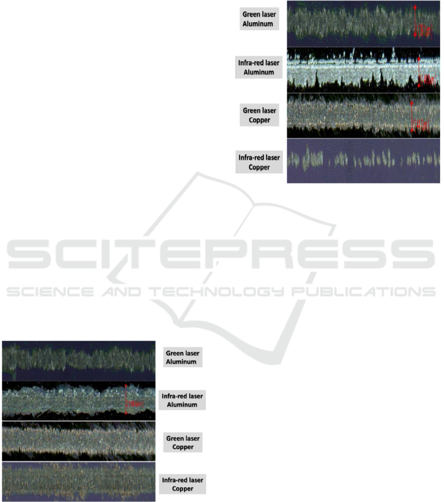
photo lithography techniques, main advantages
include higher flexibility, minimal number of
process steps and also no requirements of masks. An
Infra-red Nd:YAG laser with 8 picosecond pulse
duration and frequency doubled (λ=515 nm) are
used for tests. Photons are more energetic with
shorter laser wavelengths and they are easier to be
absorbed by the materials than photons with longer
wavelengths. To decrease the permeation of particles
in test substrate and to prevent the diffusion and
desorption stages in thin film production, additional
high density inorganic layer is used to control the
process in adsorption and absorption in deposition
level (Lianwei, 2014 and Salminen, 2013). High
laser power with short pulses cause very little
thermal influence on the substrate. As it can be seen
in Figure1 (a) and (b), four lines are made with laser
direct writing method. Distance between each laser
shot has been optimized by 10µm, 9 pulses per each
position and the 100 KHz repetition rate for left and
40 KHz for the right pictures. Pulse energy for both
lasers with 40 KHz repetition rate is measured as
137 µJ. The first line in the picture is made by
aluminium particles as donor with frequency
doubled laser (λ=515nm) which are deposited on the
substrate. In the second line infrared laser (λ=1064)
is used for aluminium particles as well. In the third
and fourth lines, copper is used for positioning of
nano particles with green and IR laser respectively.
The pulse energy of the IR laser for aluminium and
copper with 100 KHz repetition rate and 7W output
power is calculated as: 69.5 µJ. The laser intensity
with 1.064 µm wavelength for aluminium and
copper was: 245 KW/cm².
Figure 1(a): Deposition of Al & Cu by laser wavelengths-
100 KHz repetition rate.
The silicon wafer has passivized by silicon
nitride layer in order to decrease the permeation of
particles in Si-wafer substrates and to prevent
diffusion phenomenon. The coating thickness of
aluminium and copper was 500nm on a normal
glass with 250mm diameter and 1.1mm thickness.
Figure 1(b): Deposition of Al & Cu by laser wavelengths-
40 KHz repetition rate.
3 OPTIMIZING PULSES PER
SHOT AND OVERLAPPING
In this step pulses per laser shot are subject to
optimization. It was determined that a repetition rate
of greater than 80 KHz achieves good results
(Azhdast, 2015; 2016). Hence, a repetition rate of
100 KHz was used in this optimization step since the
overlapping has not been optimized yet, it is set to
80% for this step. The pulses per shot were changed
from 1 to 40 for deposition of Al on Si-wafer with
silicon nitride passivation. Al has a relatively high
and constant reflectance in the visible and infrared
wavelength range. Figure 2 (a) and (b) show the
results for pulses per shot in the range of 7 to 13. It
can be perceived that for less than 8 pulses per shot
the particles are not sputtered well on the substrate
in which case the samples later fail the adhesion tape
test. For 8 to 9 pulses a good deposition can be
observed. By increasing the number of pulses to
more than 15, the high energy leads to an impaired
layer on the substrate. The findings from Al can be
confirmed on Cu as optimal results are found for 8
to 9 pulses per shot as well.
Optimization Parameters for Laser-induced Forward Transfer of Al and Cu on Si-wafer Substrate
229
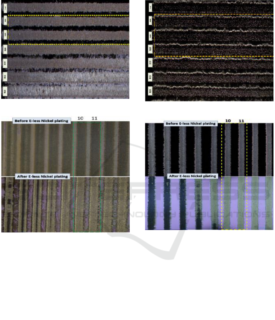
Figure 2(a): Pulses per shot in Aluminium.
Figure 2(b): Pulses per shot in Copper.
Finally the overlapping is subject to
optimization. Knowing from the previous step that 9
pulses per shot achieve good results, this parameter
setting was used in this step. The distance between
shots is changed from 1-40 µm.
Figures 3 illustrate that a distance of 10-11µm
produces perfect lines with smooth edges. The lines
are nickel plated in place of better coalescence. For
distances well above 20µm distortion on the edges
can be clearly noticed. The optimal distance between
shots for copper is very similar as shown in figure
3(b). It can be concluded that 80% overlapping
guarantees the production of perfect lines. With less
than 10µm distances between each laser shot, the
lines have more overlap which can be seen in the
pictures after nickel plating. The diffusion layer
occurs when the distances between each laser pulses
are too less.
Figure 3(a): Overlapping of laser shots; Aluminium.
Figure 3(b): Overlapping of laser shots; Copper.
4 CONCLUSIONS
A large number of techniques can be implemented to
precipitate a thin layer of film on a surface. Pulsed
laser energy should be higher than the threshold
energy in order to have the transmission of particles
from the coated side of the glass in/on to the target.
The chosen technique of thousand seeds, allow for
further investigation and additional optimization. It
has been found that the smallest features which are
ablated from a donor, obtained at a fluence level just
above the printing threshold for the sample. This
printing threshold is dependent on the sample
thickness, quality of focus, and duration of the laser
pulse as well as laser intensity. Copper in
comparison with aluminium, has a good wettability
for both different laser wavelengths. Nevertheless,
too high pulse energy at 40 KHz makes an uneven
PHOTOPTICS 2018 - 6th International Conference on Photonics, Optics and Laser Technology
230

implanted surface. It is obvious that the quality of
lines with lower intensity is not as well as higher
ones. The higher laser intensity would cause more
permeation of particles in the solid membrane and
makes desorption structure of the layer. The printing
threshold for the 500 nm thick donor sample for
copper and aluminium were found to be 83 µJ and
87µJ for the 8 ps pulses respectively.
REFERENCES
Azhdast M. H, 2017. Comparison of nano particle
implantation with picosecond lasers by concerning
different wavelengths from Aluminum and Copper on
Silicon wafer substrate, Conference on Lasers and
Electro-Optics, OSA Technical Digest.
Golnaz B. J., 2008. Investigation of the near surface
mechanical properties of Au-Ti thin films,” Master
thesis, Oklahoma State University.
Azhdast M. H., 2017. Deposition of Al and Cu
nanoparticles on Silicon Wafer using a Picosecond
Nd:YAG Laser: An Experiment-based Parameter
Optimization Guide, Conference on Lasers and
Electro-Optics, OSA Technical Digest.
S Bera S., 2007, Optimization study of the femtosecond
laser-induced forward-transfer process with thin
aluminum films, Appl. Opt. 46, 4650-4659.
Wartena R, 2004., Li-ion microbatteries generated by a
laser direct-write method, Nava research Laboratory,
Journal of Power Sources 126 193–202.
Lianwei C., 2014. Tuning Optical Nonlinearity of Laser-
Ablation-Synthesized Silicon Nanoparticles via
Doping Concentration, Journal of Nanomaterial,
National University of Singapore, Singapore.
Salminen T., 2013. Production of nanomaterial by pulsed
laser ablation, PhD thesis, Tampere University of
technology, Tampere, Finland.
Azhdast M.H., 2015. Arrangement for applying
conductive nanoparticles onto a substrate, Patent
publication number: WO2015117872A1.
Azhdast M. H., 2016. Adhesion mechanism between laser
sputtered Aluminum nano particles on Si-Wafer by
Nd:YAG laser, Conference on Lasers and Electro-
Optics, OSA Technical Digest.
Azhdast M.H., 2015. Nano particle production by laser
ablation and metal sputtering on Si-Wafer substrate,
Conference on Lasers and Electro-Optics, OSA
Technical Digest.
Craig B., 2007. Laser Direct-Write Techniques for
Printing of Complex Materials, MRS BULLETIN, Vol.
32.
Pique A., 2008. Laser Decal Transfer of Electronic
Materials with Thin Film Characteristics, Naval
Research Laboratory, 4555 Overlook Avenue, SW,
Washington, DC, USA 20375
Optimization Parameters for Laser-induced Forward Transfer of Al and Cu on Si-wafer Substrate
231
