
Design, Ion Beam Fabrication and Test of Integrated Optical
Elements
I. Bányász
1
, S. Pelli
2,3
, G. Nunzi-Conti
2
, G. C. Righini
3
, S. Berneschi
2
, E. Szilágyi
1
, A. Németh
1
,
M. Fried
4,5
, P. Petrik
4
, E. Agócs
4
, B. Kalas
4
, Z. Zolnai
4
, N. Q. Khanh
4
, I. Rajta
6
, G. U. L. Nagy
6
,
V. Havranek
7
, V. Vosecek
7
, M. Veres
8
, L. Himics
8
1
Department of Nuclear Materials Science, Wigner Research Centre for Physics, Hungarian Academy of Sciences,
P.O.B. 49, H-1525, Budapest, Hungary
2
MDF-Lab, “Nello Carrara” Institute of Applied Physics, IFAC-CNR, Via Madonna del Piano 10,
50019 Sesto Fiorentino (FI), Italy
3
“Enrico Fermi” Center for Study and Research, Piazza del Viminale 2, 00184 Roma, Italy
4
Research Institute for Technical Physics and Materials Science, Centre for Energy Research,
Hungarian Academy of Sciences, Budapest, P.O.B. 49, H-1525, Hungary
5
Institute of Microelectronics and Technology, Óbuda University, Tavaszmező u. 17, H-1084 Budapest, Hungary
6
MTA Atomki, Institute for Nuclear Research, Hungarian Academy of Sciences, H-4001 Debrecen, P.O. Box 51, Hungary
7
Nuclear Physics Institute AV CR, Řež near Prague, 250 68, Czech Republic
8
Department of Applied and Nonlinear Optics, Wigner Research Centre for Physics, Hungarian Academy of Sciences,
P.O.B. 49, H-1525, Budapest, Hungary
Keywords: Ion Implantation, Integrated Optics, Optical Planar Waveguide, Optical Channel Waveguide, Optical Grating,
M-Line Spectroscopy, Spectroscopic Ellipsometry, Micro Raman Spectroscopy, Rutherford Backscattering.
Abstract: Various methods, based on the use of ion beams, were used for the fabrication of planar and channel optical
waveguides and Bragg gratings in optical crystals and glasses. Some examples of the results of these
researches are presented in this review. Researches were initiated on ion beam fabrication of planar and
channel optical waveguides in tellurite glasses. The ions used in the experiments were mainly helium, carbon,
nitrogen and oxygen. In case of the two dimensional elements, like channel waveguides, both masked ion
implantation and direct writing with ion microbeam were used. Optical microscopy (phase contrast,
interference and interference contrast (INTERPHAKO), spectroscopic ellipsometry, m-line spectroscopy,
Rutherford Backscattering and micro Raman spectroscopy were used to test the integrated optical elements.
1 INTRODUCTION
Realization of light confinement in optical guiding
structures, both longitudinally and transversally,
represented the milestone for the development of
Integrated Optics (IO) devices of various
functionalities, like optical amplification and light
coupling or splitting, coexisting in a same chip
(Miller, 1969 and Jaouen, 1999). Currently, the main
effort in this field, coming from the research is that of
discovering and developing the best materials –
fabrication processes combination in order to reduce
the cost and increase the performance of the
previously mentioned devices. Glasses and crystals,
because of their physical and optical properties,
continue to find an even more increasing interest in
different technology fields. Generally, glasses with
their amorphous structure and relatively low
refractive better interface with the optical fiber, thus
resulting in lower values of coupling losses in the
optical devices (Li, 2011 and Zou, 2001).
Glasses doped with Rare Earth (RE) ions are still
the best choice for the development of integrated
optical amplifiers where the request of a flat gain in a
broader bandwidth is well satisfied by the disordered
structure of these materials (Ogoshi, 2000 and Ohishi,
1998). Crystalline materials with their nonlinear
properties and possibility of refractive index
modulation by different effects, such as electro-
optical and/or thermo – optical, are strongly used in
different fields of the optoelectronics (Wooten, 2000
and Xu, 2015). Due to their ordered structure, these
materials represent a suitable RE host for the
Bányász, I., Pelli, S., Nunzi-Conti, G., Righini, G., Berneschi, S., Szilágyi, E., Németh, A., Fried, M., Petrik, P., Agócs, E., Kalas, B., Zolnai, Z., Khanh, N., Rajta, I., Nagy, G., Havranek, V.,
Vosecek, V., Veres, M. and Himics, L.
Design, Ion Beam Fabrication and Test of Integrated Optical Elements .
DOI: 10.5220/0006679002790285
In Proceedings of the 6th International Conference on Photonics, Optics and Laser Technology (PHOTOPTICS 2018), pages 279-285
ISBN: 978-989-758-286-8
Copyright © 2018 by SCITEPRESS – Science and Technology Publications, Lda. All rights reserved
279
realization of high gain and low threshold lasing
devices (Sohler, 2005).
Ion beam irradiation, thanks to its high
controllability and reproducibility, represents a
suitable technique for the fabrication of integrated
optical elements, such as active and passive
waveguides and optical gratings, in most optical
materials. (Townsend, 1994, Chen, 2007, Chen,
2012, Peña-Rodríguez, 2012).
Buried planar and channel waveguides were
usually obtained using light ions (i.e.: protons,
helium) via increasing the index of refraction of the
target in a zone around the stopping range, which is
relatively long for these kind of ions (Ren, 2010, Yao.
2011a, Yao, 2011b and Dong, 2011).
Medium-mass ions, especially carbon and oxygen,
were also used for fabrication of optical waveguides in
amorphous and crystalline materials (Tan, 2007, Zhao,
2010, Montanari, 2012, He, 2013, Liu, 2014).
Formation of adequate refractive index changes
for waveguide fabrication with light and medium-
mass ions requires relatively high fluences, in the
10
15
-10
17
ions/cm
2
region, especially when the mass
and energy of the implanting ion are low.
The use of swift heavy ion irradiation for the
modification of the optical properties of materials was
first reported in the1990’s.
Aithal and his co-workers
irradiated organic nonlinear optical crystals with 100
MeV Ag
14+
ions, and studied optical properties of the
irradiated samples (Aithal, 1997).
Those results
opened a new possible method of fabricating optical
waveguides in the organic nonlinear optical crystals.
Opferman et al. detected formation of amorphous
tracks and layers in KTiOPO
4
crystals during
implantation with swift heavy ions at low fluences
(150 MeV Kr and 250 MeV Xe, 3·10
12
ions/cm
2
- 4·
10
13
ions/cm2) (Opfermann, 2000).
Track and
amorphous layer formation were due to electronic
interaction, and could be explained using the Gibbons
model (Gibbons, 1972). Olivares et al. reported on
implantation of LiNbO
3
crystals using 5-MeV Si
2+
,
7.5-MeV Si
2+
and 30-MeV Si
5+
ions with fluences
from 5·10
13
ions/cm
2
–1·10
15
ions/cm
2
(Olivares,
2005a). They succeeded in producing optically
isotropic amorphous layers of thicknesses increasing
with the fluence. The same group succeeded in
fabricating planar optical waveguides in LiNbO
3
crystals via implantation with 20 and 22 MeV
fluorine ions and fluences from 1·10
14
ions/cm
2
- 3·
10
15
ions/cm
2
(Olivares 2005b).
An amorphised layer
situated around the maximum of electronic stopping
power served as optical barriers while the layer left
below the crystal surface remained crystalline and
constituted the well of the optical waveguide.
2 EXPERIMENTAL
2.1 Planar Waveguides
Based on the results of our previous results of the
fabrication of low grating-constant optical gratings in
Pyrex glass with helium and nitrogen implantation in
the 500 keV – 2 MeV energy range (Bányász, 2001),
we opted for the use of nitrogen ions for the
fabrication of planar optical waveguides. We
succeeded in fabricating planar optical waveguides in
an Er-doped tungsten-tellurite oxide glass with 1.5
MeV N
+
ion implantation at fluences up to 8 ·10
16
ion/cm
2
(Berneschi, 2011).
The waveguides proved to
operative up to the wavelength of 980 nm. This was
due to the limitations caused by the small thickness of
the guiding well, 1.6 µm, calculated by the SRIM
code (Ziegler, 2004). Propagation losses in the
waveguides were reduced by thermal annealing of the
implanted samples.
Further experiments using
implantation with N
+
ions of an increased energy of
3.5 MeV resulted in planar optical waveguides in the
same glass operating up the 1550 nm
telecommunication wavelength (Bányász, 2012).
Appearance of the leaky modes in ion beam
implanted planar optical waveguides is due to the low
thickness of the barrier layer produced around the
stopping range of the implanted ions. To overcome
that problem, double-energy ion beam implantation
was used (Bányász, 2013). Design of such planar
waveguides is presented in Figures 1 and 2. The target
material was sillenite type BGO crystal (Bi
12
GeO
20
).
Double energy N
+
ion implantations were simulated
using the SRIM code. The higher energy in each case
was 3.5 MeV, the highest available energy at the one-
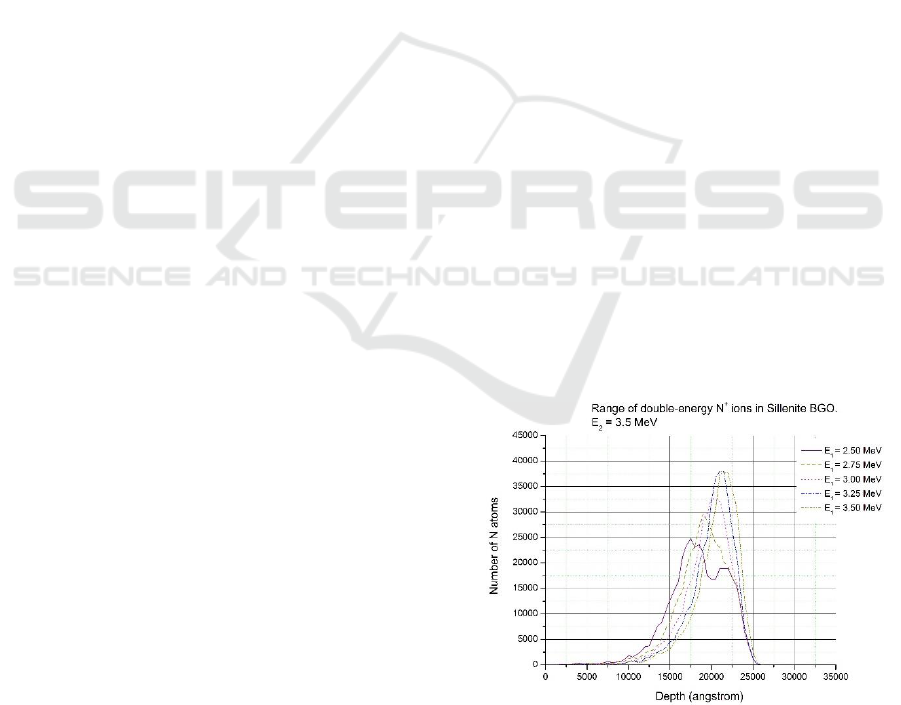
Figure 1:
Depth-distributions of the implanted N
+
ions in
sillenite type BGO crystal, calculated by the SRIM code.
Higher energy was 3.5 MeV in each case. Lower energy is
indicated in the inset.
PHOTOPTICS 2018 - 6th International Conference on Photonics, Optics and Laser Technology
280
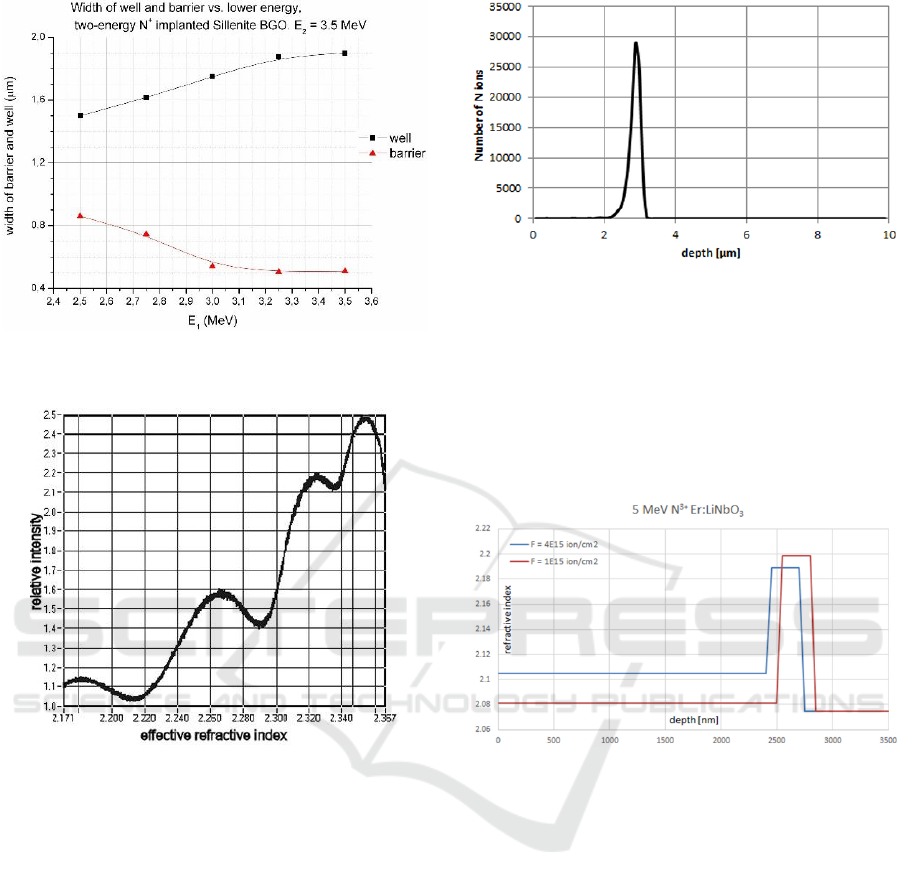
Figure 2: Width of the well and barrier layers vs. the lower
energy of irradiation in the sillenite type BGO crystal.
Figure 3: M-line spectra of the planar waveguide in sillenite
type BGO crystal, irradiated with double energy N
+
ions at
3.5 MeV and 3.1 MeV, with a fluence of 2.0· 101
6
ions/cm
2
,
taken at 1310 nm.
stage accelerator used for those experiments, while
the lower energies ranged from 2.5 to 3.25 MeV.
It can be seen in both Figures 1 and 2 that higher
implantation energy differences resulted in thicker
barrier layers and slightly reduced well thickness.
Waveguide operation at the 1310 and 1550 nm
telecommunication wavelength was demonstrated in
the planar waveguides fabricated in the Er-doped
tungsten-tellurite oxide glass and the sillenite type
BGO, see Figure 3.
With access to a modern Tandetron accelerator,
implantation with higher-mass ions at higher energies
became possible. In one of those experiments, planar
optical waveguides were formed in an Er: LiNbO
3
crystal by implantation with 5 MeV N
3+
ions.
Calculated depth distribution of the ions in the target
is shown in Figure 4.
Figure 4: Depth distribution of 5 MeV N
3+
ions in Er:
LiNbO
3
, calculated with SRIM.
The planar waveguides were studied by spectroscopic
ellipsometry using a Woollam M-2000DI spectro-
scopic ellipsometer (wavelength range of 193-1690
nm). Reconstructed refractive index profiles of two of
the waveguides are presented in Figure 5. Note
difference in barrier position, width and height.
Figure 5: Fitted refractive index profiles of two ion-
implanted planar waveguides. Er: LiNbO3 with 5 MeV N
3+
ion at fluences of 1 and 4·10
15
ion/cm
2
.
2.2 Bragg Gratings
Multi-energy ion implantation makes it possible to
fabricated optical elements structured in depth. Such
elements can be stacked planar waveguides or Bragg
gratings. Depth distribution of the implanted ions is
of flat-topped skewed Gaussian, and the position of
the peak of those curves changes monotonically with
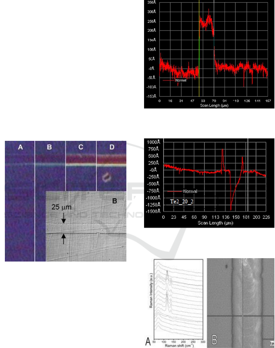
ion energy. Design of such a Bragg grating, made by
the SRIM code, is shown in Figure 6. Total thickness
of the Bragg grating was about 3 µm, grating constant
Λ = 0.5 µm.
However, depth distribution of the
damage shows only about one third of the modulation
seen in Figure 6.
Design, Ion Beam Fabrication and Test of Integrated Optical Elements
281
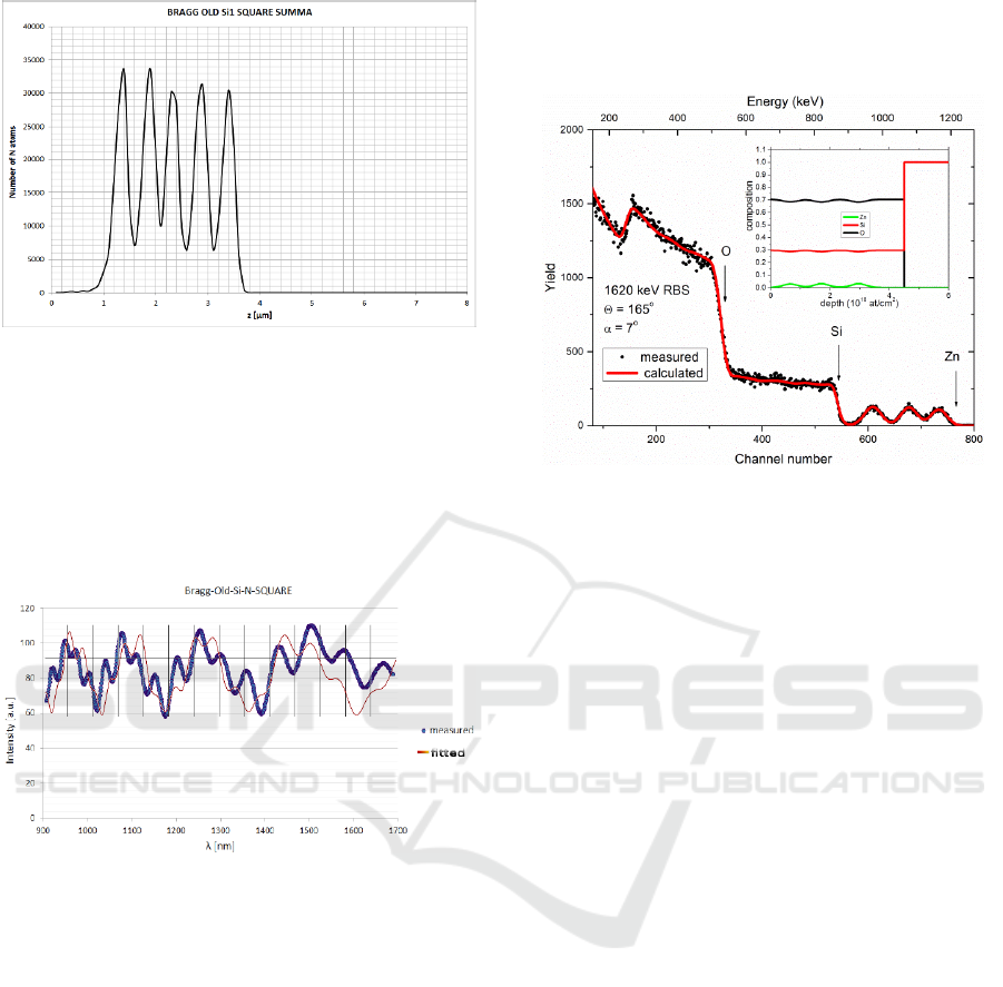
Figure 6: Calculated depth distribution of the implanted
ions across a Bragg grating in silicon. The energies were
800 keV, 1.4, 2.0, 2.75 and 3.5 MeV.
The Bragg grating was studied using NIR
reflectometry.
The results of the measurement are
presented in Figure 7. The high modulation in the
reflectivity suggests a strong refractive index
modulation in the grating.
Figure 7: Measured (points) and fitted (red line) NIR
reflectance of an ion-implanted Bragg grating. N
+
, 800 keV
< E < 3.5 MeV, Si sample, Fluence per energy: 2·10
16
ion/cm
2
.
Instead of varying the energy of the implanted
ions in a bulk target, one can fabricate ion implanted
Bragg grating in another way. One can combine the
use of relatively low-energy ions and thin film
deposition. Once a thin film of thickness
corresponding to the designed grating constant of the
Bragg grating is deposited on a substrate, it is
implanted with low-energy ions of a suitable energy
to obtain an ion distribution centered at the middle of
the layer. Then the whole procedure is repeated until
the desired total thickness of the Bragg grating is
reached.
Similarly, to the previous method, stacking
of the ion-implanted thin layers can result in a quasi-
sinusoidal depth profile of the refractive index.
Such Bragg gratings were prepared in SiO
2
thin
films, both on silicon and glass substrates. The Bragg
gratings were studied by Rutherford Backscattering
Spectrometry (RBS). The results of the RBS study
can be seen in Figure 8.
Figure 8: RBS measurement of an ion implanted Bragg
grating.
The sample was prepared by repeating Chemical
Vapor Deposition (CVD) of SiO
2
thin layers (first
300 nm and then twice 200 nm) and low-energy ion
implantation of each layer by 130 keV Zn
+
ions on a
silicon substrate. Both the measured and simulated
RBS spectrum spectra and the calculated depth
distribution (inset) of Zn in the sample show regular
quasi-sinusoidal distributions. The high implanted
fluences (2·10
16
ions/cm
2
each) resulted in about 3 %
peak Zn concentration (see inset).
That concentration
implies high modulation of the refractive index, so
that even a low number of implanted grating layers
could result in high diffraction efficiency.
Diffraction efficiency measurements of the
various ion implanted Bragg gratings are under way.
2.3 Channel Waveguides
Two basic methods were used for the fabrication of
channel waveguides in Er-Te glass, eulytine and
sillenite type BGO crystals, CaF
2
, LiNbO
3
and other
optical crystals. The first one was implantation
through masks. Various masks were used, such as a
special silicon membrane mask that contained 24 μm
wide slits and a patterned thick AZ4562 photoresist
layer on the surface of the sample. The thickness of
the channel waveguides was between 5 μm and 24
μm.
Experiments using both methods were also
carried out at the van de Graaff accelerator of the
Wigner Research Centre for Physics, using N
+
ions at
energies of 1.5 MeV and 3.5 MeV.
The second method was direct the writing of 15-
µm channel waveguides in Er-Te glass with carbon,
PHOTOPTICS 2018 - 6th International Conference on Photonics, Optics and Laser Technology
282
oxygen and nitrogen microbeams of low (around 5
MeV) and high (around 10 MeV) using a 3-MV
Tandetron 4130 MC (High Voltage Engineering
Europa B.V.) accelerator with a quadrupole triplet
OM150 Oxford Microbeams Ltd. at the Řež Nuclear
Physics Institute, Czech Republic.
Design of channel waveguides was similar to that
of the planar ones. However, lateral confinement in
the ion-implanted channel waveguides was not
always automatically ensured in the experiments.
The first working channel waveguides were
obtained in an Er: tungsten-tellurite glass, using a
thick silicon membrane with 24 µm wide slits and
implantation with 1.5 MeV energy N
+
ions
(Berneschi, 2007). Guiding up to λ = 980 nm was
demonstrated.
Green upconversion at the same
wavelength was also observed.
Interference phase
contrast (INTERPHAKO) microphotos of the
channel waveguides are shown in Figure 9.
Figure 9: Interference phase contrast microscopic image of
1.5 MeV N
+
irradiated channel waveguides. Fluence was
0.5, 1, 2 and 4∙10
16
/cm
2
for waveguides A, B, C and D.
Inset: Conventional microscopic image of waveguide B.
In Figure 9, higher difference in hue corresponds
to a higher difference in optical path, and hence
refractive index modulation in the ion-implanted
channel waveguides.
Profilometric scans (performed by a Talysurf
device) of the ion implanted channel waveguides
revealed that, depending on the implanted fluence, a
swelling or depression of the implanted surface can
occur. The results are shown in Figures 10 and 11.
Just a two-fold increase in fluence drastically
changed the sign and profile of the surface change
across the ion-implanted channel waveguide.
Figure 10: Profilometric scan across an ion implanted
channel waveguide. Implantation: 1.5 MeV energy N
+
ions,
fluence = 1∙10
16
ions/cm
2
.
Rectangular ridge, h = 25 nm.
Figure 11: Profilometric scan across an ion implanted
channel waveguide. Implantation: 1.5 MeV energy N
+
ions,
fluence = 2∙10
16
ions/cm
2
. Triangular groove, h = 125 nm.
Figure 12: Micro Raman spectra (A) taken across a channel
waveguide (B) fabricated in an Er-Te glass with 3.5 MeV
N
3+
ion irradiation through a silicon mask. Parameter of the
curves is laser microbeam position along the horizontal line
in the microphotograph.
Design, Ion Beam Fabrication and Test of Integrated Optical Elements
283
More recently, the same method was used to
fabricate channel waveguides in the same Er:
tungsten-tellurite glass, but with N
+
ions of 3.5 MeV
energy. Functionality tests of those channel
waveguides are under way. The channel waveguides
were also studied using micro Raman spectroscopy.
Result of such a measurement is shown in Figure 12.
Note the appearance of new Raman lines in the
implanted region, as very prominent manifestation of
the structural changes caused in the target by the ion
implantation.
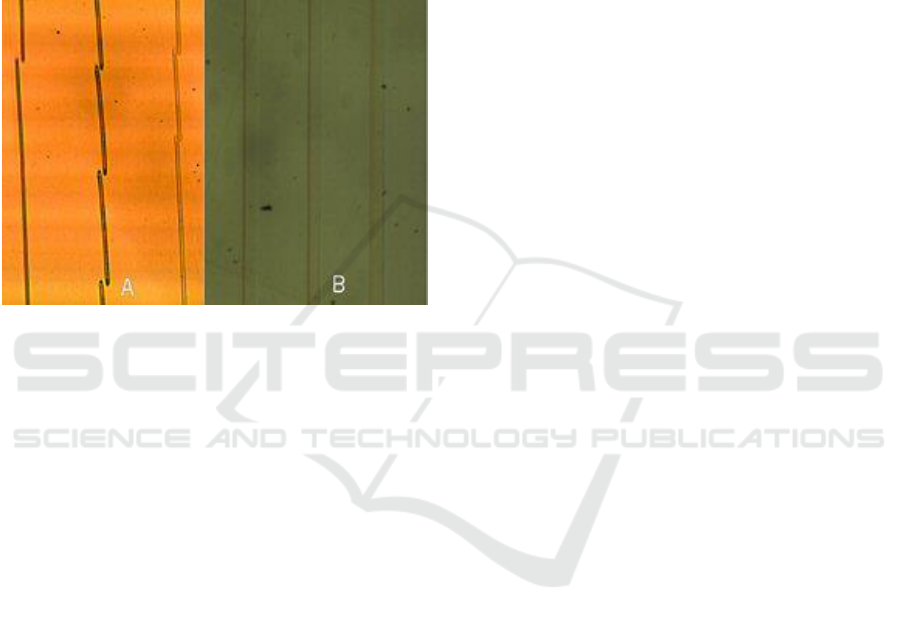
Figure 13: INTERPHAKO microphotographs of channel
waveguides written in Er-Te glass with 6 MeV C
3+
microbeam without charge compensation (A) and with an
electron source (B).
As for the direct writing of channel waveguides, a
number of samples have been completed so far, and
functionality tests are under way. Just to illustrate the
practical difficulties arising in such experiments,
microscopic photographs of two sets of focused ion
beam written channel waveguides are presented in
Figure 13.
It can be seen that in the absence of charge
compensation the electric field of the charge
accumulating on the surface of the sample
periodically deviates the ion microbeam, resulting in
broken channel waveguides (Figure 13 A). After
installing an electron source in the vacuum chamber
charge accumulation was eliminated, and contiguous
channel waveguides could be written (Figure 13 B).
3 CONCLUSION
It was proved that various integrated optical elements
could be fabricated with ion implantation, using
medium-mass ions, such as carbon, nitrogen and
oxygen of energies in the 1–10 MeV range. Planar
and channel optical waveguides and Bragg gratings
were fabricated by the ion beam techniques. The
optical elements were prepared in a number of optical
crystals and glasses, e.g. sillenite and eulytine type
BGO, doped and undoped LiNbO
3
, SiO
2
, Si and Er: -
tungsten-tellurite glass.
As for the results with ion
implanted planar waveguides, it was found that
nitrogen ion implantation resulted in higher refractive
index contrasts and hence better confinement than the
previously widely used proton and helium ion
implantation. It proved to give even better results in
several materials than carbon and oxygen
implantation. Double-energy implantation was
successfully adapted in those experiments to produce
wider barriers and suppress leaky modes.
Thermal
annealing was used to eliminate or reduce lattice
damages caused by the implantation and reduce
propagation losses. Operation at telecommunication
wavelengths of 1310 and 1550 nm was demonstrated
in the waveguides written in the majority of the glass
and crystalline materials studied. It was demonstrated
that Bragg gratings of quasi-sinusoidal profile could
be fabricated in glasses and crystals either by multi-
energy implantation with MeV energy ions or by the
combination of the growth of a stack of thin films and
successive implantation of low-energy (50–100 keV)
ions in each layer. In principle, high diffraction
efficiency could be achieved with such gratings
consisting of a relatively low number of grating
periods, and having a moderate refractive index
modulation. Ion beam implantation through special
masks and direct writing with medium- to high-
energy focused beams of medium-mass ions was
proposed and used for the fabrication of channel
waveguides. The first channel waveguides fabricated
in an Er: -tungsten-tellurite glass by implantation
through mask operated up to the wavelength of 980
nm. Although evaluation of a large part of the ion
beam implanted optical elements is still under way,
the results so far confirmed show that ion beam
fabrication is an adequate method for fabrication of
various types of optical elements. The use of swift
heavy ions is an especially promising method, since
it requires very low fluences (down to 10
11
ions/cm
2
),
corresponding to short processing times.
ACKNOWLEDGEMENTS
This work was supported by the following funds:
Hungarian National Research Fund, Project Number
OTKA 115852. Part of this work has been carried out
at the CANAM (Centre of Accelerators and
Nuclear
Analytical Methods) infrastructure LM 2015056.
This publication was supported by the OP RDE,
PHOTOPTICS 2018 - 6th International Conference on Photonics, Optics and Laser Technology
284

MEYS, and Czech Republic under the project
CANAM OP, CZ.02.1.01/0.0/0.0/16_013/0001812.
REFERENCES
Aithal, P. Sreeramana, Nagaraja, H. S., Mohan Rao, P,
Avasthi, D. K., and Sarma, Asati, Journal of Applied
Physics 81, 7526 (1997); doi: 10.1063/1.365294
Bányász, I., Fried, M., Dücső, Cs., and Vértesy, Z., Appl.
Phys. Lett., 79, 3755 (2001)
Bányász, I., S. Berneschi, M. Bettinelli, M. Brenci, et al.,
“MeV energy N
+
- implanted planar optical waveguides
in Er-doped tungsten-tellurite glass operating at 1.55
µm”, IEEE Photonics Journal, Volume 4, Issue 3, pp.
721-7, DOI: 10.1109/JPHOT.2012.2194997 (2012)
Bányász, I., Z. Zolnai, M. Fried, T. Lohner, et al., “Single -
and double energy N
+
ion irradiated planar optical
waveguides in Er: Tungsten-Tellurite Oxide glass and
sillenite type Bismuth Germanate crystals for telecom
applications”, Nuclear Instruments and Methods in
Physics Research Section B, 307, 299-304 (2013)
Berneschi, S., G. Nunzi Conti, I. Bányász, et al., “Ion beam
irradiated channel waveguides in Er
3+
-doped tellurite
glass", Applied Physics Letters, 90, 121136, (2007)
Berneschi, S, Brenci, M., Nunzi Conti, G., Pelli, S., et al.,
Slab optical waveguides in Er
3+
-doped tellurite glass by
N
+
ion implantation at 1.5 MeV, Optical Engineering,
50, 071110 (2011).
Chen, F.,
Wang, Xue-Lin and Wang, Ke-Ming, Opt. Mat.,
29, 1523-1542, DOI: 10.1016/j.optmat.2006.08.001
(2007).
Dong, N., Jaque, D., Chen, F. and Lu, Q., “Second
harmonic and Raman imaging of He
+
implanted
KTiOPO4 waveguides”, Optics Express, 19, 13934-
13939 (2011).
Gibbons, J.F., Proceedings of the IEEE, 60, 1062 – 1096,
(1972), DOI: 10.1109/PROC.1972.8854
He, Ruiyun, Shuqian Sun, Miaomiao Xu, Feng Chen,
Shavkat Akhmadaliev, Shengqiang Zhou, Nucl. Instr.
and Meth. in Phys. Res. B, 308, 6-8 (2013)
Li, S.- L. Han, P., Shi, M., Yao, Y., et al., “Low-loss
channel optical waveguide fabrication in Nd
3+
-doped
silicate glasses by femtosecond laser direct writing”,
Optics Express, 19, 23958-23964 (2011).
Liu Chun-Xiao; Xu Jun; Xu Xiao-Li; Wu Shu; Wei Wei;
Guo Hai-Tao; Li Wei-Nan; and Peng Bo, Optical
Engineering, 53(3), 037101 (2014)
Jaouen, Y., du Mouza, L., Barbier, D. Delavaux, J., Bruno,
P., “Eight-wavelength Er-Yb doped amplifier:
combiner/splitter planar integrated module”, IEEE
Photonics Technology Letters, 11, 1105 – 1107 (1999).
Miller, S. E. “Integrated Optics: An introduction”, Bell
System Technical Journal, 48, 2059 – 2069 (1969).
Ogoshi, H., Ichino, S. and Kurotori, K., “Broadband Optical
Amplifiers for DWDM Systems”, Furukawa Review,
No. 19, 17-21 (2000).
Ohishi, Y., Mori, A., Yamada, M., Ono, H., et al., “Gain
characteristics of tellurite-based erbium-doped fiber
amplifiers for 1.5 μm broadband amplification”, Optics
Letters, 23, 274-276 (1998).
Olivares, J., García, G., Agulló-López, F., Agulló-Rueda,
F., Kling, A., Soares, J.C., Appl. Phys. A, 81, 1465–
1469 (2005) DOI: 10.1007/s00339-005-3237-x
Olivares, J., García, García-Navarro, Agulló-López, F., A.,
Caballero, O., García-Cabañes, A, Appl. Phys. Lett., 86,
183501 (2005)
Opfermann, Th., Höche, Klaumünzer, S., Wesch, W, Nucl.
Instr. and Meth. in Phys. Res. B, 166-167, 954-958
(2000)
Peña-Rodríguez, O., Olivares, J., Carrascosa, M., García-
Cabañes, A., Rivera A. and Agulló-López, F., “Optical
Waveguides Fabricated by Ion Implantations/Ir-
radiation: A Review”, in: Ion Implantation, Prof. Mark
Goorsky (Ed.), ISBN: 978-953-51-0634-0, InTech,
Available from: http://www.intechopen.com/books/
ion-implantations/optical-waveguides-fabricated-by-
ion-implantation-irradiation-a-review (2012)
Ren, Y., Tan, Y., Chen, F., Jaque, D., et al, “Optical channel
waveguides in Nd: LGS laser crystals produced by
proton implantation”, Optics Express, 18, 16258-16263
(2010).
Sohler, W., Das, B., Dey, D., Reza, S., et al., “Erbium-
Doped Lithium Niobate Waveguide Lasers”, IEICE
Trans. Electron., E88-C, 990-997 (2005).
Tan Y, Chen F, Physica Status Solidi-Rapid Research
Letters 1 (6), 277-279 (2007)
Townsend, P. D., Chandler, P. J.
and Zhang, L., Optical
Effects of Ion Implantation, Cambridge University
Press, Cambridge, U.K. (1994)
Xu, Kaikai, Liu, Haitao and Zhang, Zhengyuan, “Gate-
controlled diode structure based electro-optical
interfaces in standard silicon-CMOS integrated
circuitry”, Applied Optics, 54, 6420-6424 (2015)
Yao, Y., Tan, Y., Dong, N., Chen, F. and Bettiol, A. A.,
“Continuous wave Nd: YAG channel waveguide laser
produced by focused proton beam writing”, Optics
Express, 18, 24516-24521 (2011).
Yao, Y., Dong, N., Chen, Vanga, S. K.
and Bettiol, A. A.,
“Proton beam writing of Nd: GGG crystals as new
waveguide laser sources”, Optics Letters, 36 4173-4175
(2011).
Wooten, E. L.
et al., “A Review of Lithium Niobate
Modulators for Fiber-Optic Communications
Systems”, IEEE Journal of Selected Topics in Quantum
Electronics, 6, 69-82 (2000).
Zhao, Jin-Hua, Liu, Xiu-Hong, Huang, Qing, Liu, Peng,
Wang Lei and Wang, Xue-Lin, Nuclear Instruments
and Methods in Physics Research Section B: Beam
Interactions with Materials and Atoms, 268, 2923–
2925 (2010)
Ziegler, J.F., “SRIM-2003”, Nucl. Instr. and Meth.B, 219–
220, 1027 (2004), and http://www.srim.org
Zou, J., Zhao, F. and Chen, R. T., “Two-step K
+
-Na
+
and
Ag
+
-Na
+
ion-exchanged glass waveguides for C-band
applications”, Applied Optics, 41, 7620-7626 (2002).
Design, Ion Beam Fabrication and Test of Integrated Optical Elements
285
