
Column Scan Optimization by Increasing Intra-Instruction Parallelism
Nusrat Jahan Lisa
1
, Annett Ungeth
¨
um
1
, Dirk Habich
1
, Nguyen Duy Anh Tuan
2
,
Akash Kumar
2
and Wolfgang Lehner
1
1
Database Systems Group, Technische Universit
¨
at Dresden, Dresden, Germany
2
Processor Design Group, Technische Universit
¨
at Dresden, Dresden, Germany
Keywords:
Column Stores, Scan Operation, Vectorization, FPGA, Pipeline.
Abstract:
The key objective of database systems is to reliably manage data, whereby high query throughput and low
query latency are core requirements. To satisfy these requirements for analytical query workloads, in-memory
column store database systems are state-of-the-art. In these systems, relational tables are organized by column
rather than by row, so that a full column scan is a fundamental key operation and thus, the optimization of the
key operation is very crucial. For this reason, we investigated the optimization of a well-known scan technique
using SIMD (Single Instruction Multiple Data) vectorization as well as using Field Programmable Gate Arrays
(FPGA). In this paper, we present both optimization approaches with the goal to increase the intra-instruction
execution parallelism to process more columns values in a single instruction simultaneously. For both, we
present selective results of our exhaustive evaluation. Based on this evaluation, we draw some lessons learned
for our ongoing research activities.
1 INTRODUCTION
Processing of complex analytical database queries
with low-latency and high throughput on an ever-
increasing amount of data is a major challenge in
our data-driven world. To tackle that challenge, the
database architecture shifted from a disk-oriented to a
main memory-oriented approach (Abadi et al., 2006;
Boncz et al., 2008) due to the availability of high
main memory capacities on modern hardware sys-
tems. This in-memory architecture is now state-of-
the-art and characterized by the fact, that all rele-
vant data is completely stored and processed in main
memory. Additionally, relational tables are organized
by column rather than by row (Stonebraker et al.,
2005; Boncz et al., 2008) and the traditional tuple-at-
a-time query processing model was replaced by newer
and adapted processing models like column-at-a-time
or vector-at-a-time (Stonebraker et al., 2005; Boncz
et al., 2008). To further increase the performance
of analytical queries, two key aspects play an impor-
tant role in these so-called column store database sys-
tems. On the one hand, data compression is used
to reduce the amount of data (Abadi et al., 2006;
Hildebrandt et al., 2016; Zukowski et al., 2006). On
the other hand, in-memory column stores constantly
adapt to novel hardware features like vectorization
using SIMD extensions (Polychroniou et al., 2015;
Zhou and Ross, 2002), GPUs (He et al., 2014), FP-
GAs (Sidler et al., 2017b; Teubner and Woods, 2013a)
or non-volatile main memory (Oukid et al., 2017).
A key primitive in these systems is a column
scan (Feng et al., 2015; Li and Patel, 2013; Will-
halm et al., 2009), because analytical queries usu-
ally compute aggregations over full or large parts of
columns. Thus, the optimization of the scan prim-
itive is very crucial (Feng et al., 2015; Li and Pa-
tel, 2013; Willhalm et al., 2009). Generally, the
task of a column scan is to compare each entry of a
given column against a given predicate and to return
all matching entries. To efficiently realize this col-
umn scan, Li et al. (Li and Patel, 2013) proposed a
novel technique called BitWeaving which exploits the
intra-instruction parallelism at the bit-level of mod-
ern processors. Intra-instruction parallelism means
that multiple column entries are processed by a sin-
gle instruction at once. In their horizontal approach,
multiple compressed column values are packed hori-
zontally into processor words providing high perfor-
mance when fetching the entire column value (Li and
Patel, 2013). As the authors have shown, the more
column values are packed in a processor word, the
better the BitWeaving scan performance (Li and Pa-
tel, 2013).
Unfortunately, the length of processor words is
currently fixed to 64-bit in common processors, which
344
Lisa, N., Ungethüm, A., Habich, D., Tuan, N., Kumar, A. and Lehner, W.
Column Scan Optimization by Increasing Intra-Instruction Parallelism.
DOI: 10.5220/0006897003440353
In Proceedings of the 7th International Conference on Data Science, Technology and Applications (DATA 2018), pages 344-353
ISBN: 978-989-758-318-6
Copyright © 2018 by SCITEPRESS – Science and Technology Publications, Lda. All rights reserved
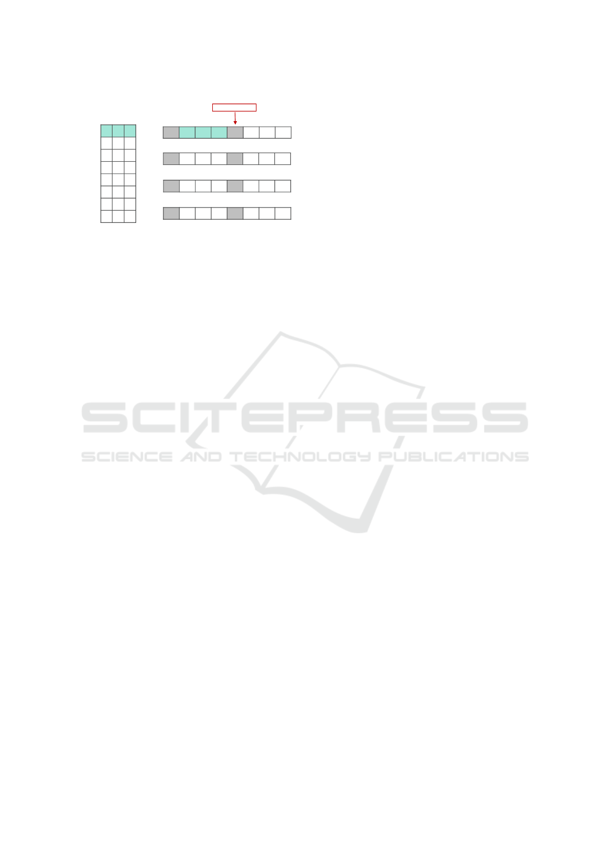
1
(b) Horizontal Storage Layout
C
3
C
4
H
2
0 1 1 0 0 1 0 0
C
5
C
6
H
3
0 0 0 1 0 1 0 0
C
7
C
8
H
4
0 1 1 0 0 1 1 0
Delimiter Bit
C
1
C
2
H
1
0 0 0 1 0 0 1 1
C
1
= 1 0 0 1
C
2
= 3 0 1 1
C
3
= 6 1 1 0
C
4
= 4 1 0 0
C
5
= 1 0 0 1
C
6
= 4 1 0 0
C
7
= 6 1 1 0
C
8
= 6 1 1 0
INT
Column Codes
(Length: 3-Bit)
(a)
Figure 1: BitWeaving example with (a) 8 integer val-
ues with their 3-bit codes and (b) data representation in
BitWeaving/H layout.
limits the performance of the BitWeaving scan. To
overcome this limitation and to increase the intra-
instruction parallelism for BitWeaving, there exists
two hardware-oriented opportunities. On the one
hand, Single Instruction Multiple Data (SIMD) in-
struction set extensions such as Intels SSE (Streaming
SIMD Extensions) and AVX (Advanced Vector Ex-
tensions) have been available in modern processors
for several years. SIMD instructions apply one op-
eration to multiple elements of so-called vector reg-
isters at once. The available operations include par-
allel arithmetic, logical, and shift operations as well
as permutations, whereby the size of the vector reg-
isters ranges from 128 (Intel SSE 4.2) to 512-bit (In-
tel AVX-512). These vector registers can be used in-
stead of regular processor words. On the other hand,
Field Programmable Gate Arrays (FPGAs) are an in-
teresting alternative which allows to design special-
ized hardware components with arbitrary processor
word sizes.
Our Contribution and Outline: In this paper, we
investigate both optimization opportunities. Based on
that, we make the following contributions.
1. In Section 2, we briefly recap the BitWeaving
technique as foundation for our work.
2. The optimization using SIMD vector registers is
discussed in Section 3, while Section 4 covers our
FPGA optimization.
3. In Section 5, we present selective results of our
exhaustive evaluation. In particular, we separately
evaluate each optimization, followed by a global
lessons learned summary.
Finally, we conclude the paper with related work in
Section 6 and a short conclusion in Section 7.
2 BITWEAVING
Generally, the BitWeaving technique is aligned to
columnar data and can be used as native storage orga-
nization technique in state-of-the-art in-memory col-
umn store database systems (Li and Patel, 2013). As
illustrated in Figure 1(a), BitWeaving takes each col-
umn separately and encodes the column values us-
ing a fixed-length order-preserving code (lightweight
data compression (Abadi et al., 2006; Damme et al.,
2017)), whereby the types of all values including nu-
meric and string types are encoded as an unsigned
integer code (Li and Patel, 2013). The term column
code refers to the encoded column values. To acceler-
ate column scans in such cases, BitWeaving consists
of a storage layout and an arithmetic framework for
predicate evaluations (Li and Patel, 2013).
2.1 Storage Layout
In the storage layout, the column codes of each col-
umn are viewed at the bit-level and the bits are aligned
in memory in a way that enables the exploitation of
the circuit-level intra-cycle (intra-instruction) paral-
lelism for the predicate evaluation. For that, BitWeav-
ing comes with two storage variants, a horizontal ver-
sion, BitWeaving/H, and a vertical version, BitWeav-
ing/V (Li and Patel, 2013). In this paper, we mainly
focus on BitWeaving/H, because many lightweight
data compression algorithms are designed for such a
horizontal layout (Abadi et al., 2006; Damme et al.,
2017). To convert horizontal compressed column
codes to a vertical BitWeaving layout, additional
work is required.
As illustrated in Figure 1(b), column codes
are continuously stored in processor words H
i
in
BitWeaving/H, where the most significant bit of every
code is used as a delimiter bit between adjacent col-
umn codes. In our example, we use 8-bit processor
words H
1
to H
4
, such that two 3-bit column codes fit
into one processor word including one delimiter bit
per code. The delimiter bit is used later to store the
result of a predicate evaluation query.
2.2 Predicate Evaluation
Baed on that, the task of a column scan is to compare
each column code with a constant C and to output a
bit vector indicating whether or not the correspond-
ing code satisfies the comparison condition. To effi-
ciently perform such column scans using the BitWeav-
ing/H storage layout, Li et al. (Li and Patel, 2013)
proposed an arithmetic framework to directly execute
predicate evaluations on the compressed data. There
Column Scan Optimization by Increasing Intra-Instruction Parallelism
345
Step 1:
Exclusive-OR
H
1
0
0
0
1
0
0
1
1
Step 2:
Masking1
(Addition)
Given Predicate:
C
i
= 3?
Initial Step: Horizontal Layout of Predicate Constant 3, Q
1
Step 3:
Masking2
(Exclusive-OR)
Step 4: Sum all the
Delimiter bits
H
2
0
1
1
0
0
1
0
0 H
3
0
0
0
1
0
1
0
0
H
4
0
1
1
0
0
1
1
0
Q
1
0
0
1
1
0
0
1
1
Q
1
0
0
1
1
0
0
1
1 Q
1
0
0
1
1
0
0
1
1 Q
1
0
0
1
1
0
0
1
1
Q
1
0
0
1
1
0
0
1
1
0
0
1
0
0
0
0
0
0
1
0
1
0
1
1
1
0
0
1
0
0
1
1
1
0
1
0
1
0
1
0
1
M
1
0
1
1
1
0
1
1
1 M
1
0
1
1
1
0
1
1
1 M
1
0
1
1
1
0
1
1
1
M
1
0
1
1
1
0
1
1
1
1
0
0
1
0
1
1
1
1
1
0
0
1
1
1
0
1
0
0
1
1
1
1
0
1
1
0
0
1
1
0
0
M
2
1
0
0
0
1
0
0
0 M
2
1
0
0
0
1
0
0
0 M
2
1
0
0
0
1
0
0
0
M
2
1
0
0
0
1
0
0
0
0
0
0
1
1
1
1
1
0
1
0
0
0
1
1
0
0
0
0
1
0
1
1
0
0
1
0
0
0
1
0
0
0
+
1
+
0
+
0
+
0 +
0
+
0
+
0
=
1
Figure 2: Equality predicate evaluation with the BitWeaving/H technique (Li and Patel, 2013).
are two main advantages: (i) predicate evaluation is
done without decompression and (ii) multiple col-
umn codes are simultaneously processed within a sin-
gle processor word using full-word instructions (intra-
instruction parallelism) (Li and Patel, 2013). The sup-
ported predicate evaluations include equality, inequal-
ity, and range checks, whereby for each evaluation a
function consisting of arithmetical and logical opera-
tions is defined (Li and Patel, 2013).
Figure 2 highlights the equality check in an ex-
emplary way. The input from Figure 1(b) is tested
against the condition C
i
= 3. Then, the predicate eval-
uation steps are as follows:
Initially: All given column codes and the query con-
stant number 3 are converted into the BitWeav-
ing/H storage layout (H
1
, H
2
, H
3
, H
4
) and Q
1
, re-
spectively.
Step 1: An Exclusive-OR operation between the
words (H
1
, H
2
, H
3
, H
4
) and Q
1
is performed.
Step 2: Masking1 operation (Addition) between the
intermediate results of Step 1 and the M
1
mask
register (where each bit of M
1
is set to one, except
the delimiter bits) is performed.
Step 3: Masking2 operation (Exclusive-OR) be-
tween the intermediate results of Step 2 and the
M
2
mask register (where only delimiter bits of M
2
is set to one and rest of all bits are set to zero) is
performed.
Step 4 (optional): Add delimiter bits to achieve the
total count (final result).
The output is a result bit vector, with one bit per input
code that indicates if the code matches the predicate
on the column. In our example in Figure 2, only the
second code (C
2
) satisfies the predicate which is visi-
ble in the resulting bit vector.
2.3 Summary
With the increasing demand for in-memory data pro-
cessing, there is a critical need for fast scan opera-
tions (Feng et al., 2015; Li and Patel, 2013; Willhalm
et al., 2009). The BitWeaving approach addresses this
need by packing multiple codes into processor words
and applying full-word instructions for predicate eval-
uations using a well-defined arithmetic framework.
As shown in (Li and Patel, 2013), the more codes
that can be packed into a processor word, the more
codes can be processed in parallel leading to better
performance (intra-instruction parallelism). Unfortu-
nately, processors words in all common CPUs are cur-
rently fixed to 64-bit in length. To further speedup
BitWeaving, there are two interesting options. First,
this can be achieved using better compression tech-
niques, which however is algorithmically limited and
highly dependent on the data characteristics. Second,
larger processor words would be beneficial. To re-
alize larger processor words, we have two hardware-
oriented alternatives: (i) vector registers of SIMD ex-
tensions or (ii) Field Programmable Gate Arrays (FP-
GAs). Both optimization alternatives are discussed in
the following sections in detail.
3 SIMD-OPTIMIZATION
One hardware-based opportunity to optimize the
BitWeaving scan is provided by vectorization using
SIMD extensions (Single Instruction Multiple Data)
of common CPUs. Generally, SIMD instructions ap-
ply one operation to multiple elements of so-called
vector registers at once. For a long time, the vec-
tor registers were 128-bit in size. However, hard-
ware vendors have introduced new SIMD instruction
set extensions operating on wider vector registers in
recent years. For instance, Intel’s Advanced Vector
Extensions 2 (AVX2) operates on 256-bit vector reg-
isters and Intel’s AVX-512 uses even 512-bit for vec-
tor registers. The wider the vector registers, the more
data elements can be stored and processed in a single
vector.
DATA 2018 - 7th International Conference on Data Science, Technology and Applications
346
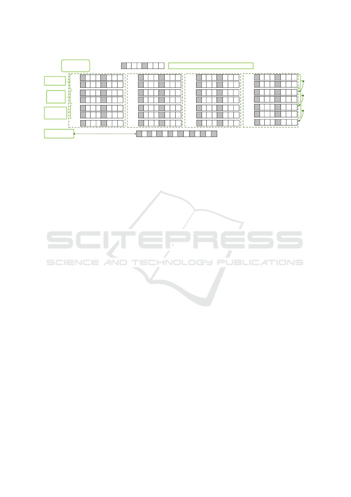
3.1 Vector Storage Layouts
A na
¨
ıve way to implement BitWeaving/H using vec-
tor extensions is to load several 64-bit values contain-
ing the column codes and delimiter bits into a vector
register. In this case, the original processor word ap-
proach is retained as proposed in BitWeaving. This
vector layout is shown as Layout 1 in Figure 3. The
evaluation works exactly as described in section 2,
but instead of arithmetic operators, the correspond-
ing SIMD instructions are used to process 2, 4, or 8
64-bit values at once. However, this method does not
use the register size optimally. For instance, in a 128-
bit register, there is space for 11 column codes with a
bit width of 10 and their delimiter bits (see Figure 3
Layout 2), but Layout 1 can only hold 10 codes. In
Layout 2, we treat the vector register as full processor
word and arrange the column codes according to the
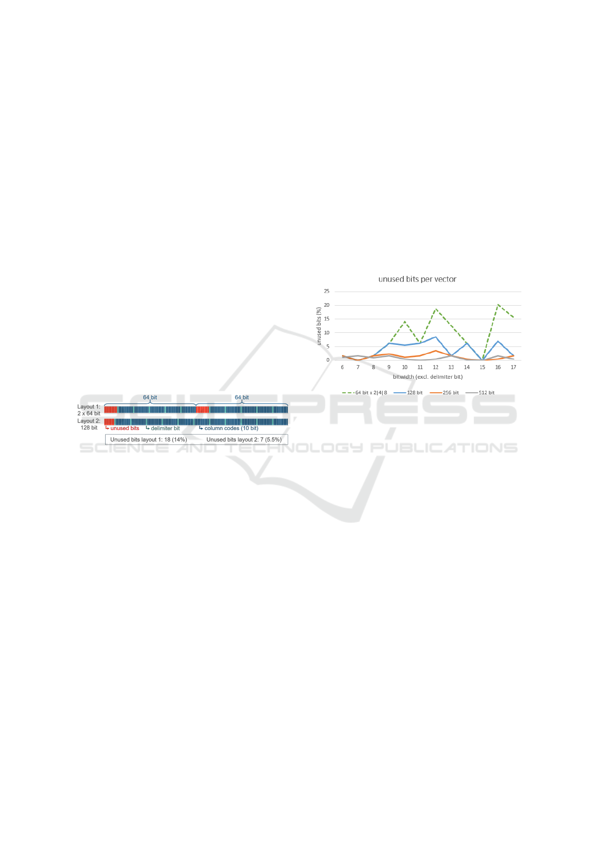
vector register size. Figure 4 shows the percentage of
unused register space for different register sizes and
both layouts, where the dashed line shows the usage
for Layout 1 and the remaining lines for Layout 2. As
we can see, Layout 2 makes better use of the vector
register. For our evaluation in Section 5, we imple-
mented both layouts.
Figure 3: Different variants to arrange column codes in a
vector register.
3.2 Predicate Evaluation
Like in the original approach, the query evaluation
on data in the BitWeaving/H layout in vector regis-
ters consists of a number of bitwise operations and
one addition. The exact bitwise operations and their
sequence depends on the comparison operator. For
instance, a smaller than comparison or an equality
check requires XOR operations and an addition as
shown in Section 2. For counting the number of re-
sults quickly, an AND is also necessary. For 512-bit
registers, this is realized by using AVX-512 intrinsics.
The following steps are necessary for a smaller than
comparison if the data is using the vector Layout 1
(see Figure 3):
1. The query constraint and the data in
a BitWeaving/H layout is loaded with
_mm512_loadu_si512. The constraint must
only be loaded once.
2. The bitwise XOR is performed with
_mm512_xor_si512.
3. The addition is performed with
_mm512_add_epi64.
4. Optional: To set only the delimiter bits, an
AND between the precomputed inverted bitmask
and the result from step 3 is performed with
_mm512_and_si512.
5. Optional: For counting the number of set delim-
iter bits _mm512_popcnt_epi64 is applied.
6. Optional: The result from step 5 can be fur-
ther reduced by adding the individual counts with
_mm512_reduce_add_epi64.
7. Finally, the result is stored with
_mm512_storeu_si512. If only the number
of results is required, this step can be skipped.
Afterwards, a new iteration starts at step 1.
Figure 4: Percentage of unused bits per vector register de-
pending on the vector layout.
Note that the SIMD intrinsics for step 5 and 6 do
not exist for 128-bit and 256-bit registers. In these
cases, the result is written back to memory and treated
conventionally, i.e. like an array of 64-bit values.
These steps work for Layout 1 but not for lay-
out 2. This is because in step 3, a full adder is re-
quired. However, this functionality is supported for
words containing 16, 32, or 64 bits, but not for 128,
256, or 512 bits. Hence, this adder must be imple-
mented by the software.
3.3 Full Adder for Large Numbers
While Layout 2 uses the size of the vector register
more efficiently, it comes with a major drawback:
There is no full adder for more than 64 bit on re-
cent CPUs. The evaluation with BitWeaving/H uses
mainly bitwise operations but one addition is neces-
sary in all evaluations, i.e. equality, greater than, and
smaller than. To realize this addition for 128, 256, or
512 bit, there are two different ways: (a) the addition
is done by iterating through the bits of the summands
and determining and adding the carry bit in every step,
and (b) only the carry at the 64-bit boundaries is de-
termined and added to the subsequent 64-bit value.
Column Scan Optimization by Increasing Intra-Instruction Parallelism
347
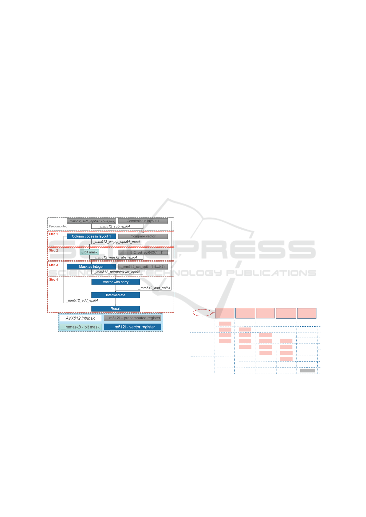
Option (a) requires sequential processing and cannot
be implemented in a vectorized way. Thus, we chose
option (b). The exact steps for option 2 are shown in
Figure 5 for 512-bit vector registers:
1. Since the result of the addition of two 64-bit val-
ues is also 64-bit, a potential overflow cannot
be determined directly. Instead, we subtract one
summand from the largest representable number
and check whether the result is larger than the
other summand. If it is smaller, there is a carry.
This can be done vectorized. The output of the
comparison between two vector registers contain-
ing unsigned 64-bit integers is a bitmask.
2. The bitmask resulting from step 1 is used on a vec-
tor containing only the decimal number 1 as 64-bit
value at every position.
3. A carry is always added to the subsequent 64-bit
value. For this reason, the result from step 2 is
shifted to the left by 64-bit. This is realized by in-
trinsics providing a permutation of 64-bit values.
4. Finally, the two summands and the result from
step 3 are added.
Figure 5: A software adder for large numbers using AVX-
512 intrinsics. For BitWeaving, the two summands are the
constraint and the column codes. This approach can easily
be adapted for 128 and 256 bits.
All steps can be done using AVX-512 intrinsics.
If one of the summands is a constant, like the con-
straint in BitWeaving, the subtraction in step 1 can be
precomputed.
3.4 Summary
As described above, the original BitWeaving/H ap-
proach can be ported to SIMD extensions in various
ways. In Section 5, we will evaluate all possibilities
in detail.
4 FPGA-OPTIMIZATION
Besides the optimization by means of wider vec-
tor registers, the second hardware-based optimization
possibility is the use of Field Programmable Gate Ar-
rays (FPGAs). FPGAs are integrated circuits, which
are configurable after being manufactured. More
specifically, a hardware description language, e.g.,
Verilog, is used to describe a custom hardware mod-
ule. This description is then translated via several
steps to an implementation for the FPGAs. From the
perspective of BitWeaving/H, the advantage of FP-
GAs is that we are able to use an arbitrary length
of processor word in our custom made BitWeaving/H
hardware.
4.1 Target FPGA System
Modern FPGAs are based on MPSoC (multiproces-
sor system on chip) architectures. The Xilinx® Zynq
UltraScale+™ platform—our target FPGA system—
is such an MPSoC-based FPGA board containing
not only programmable logic but also four ARM®
Cortex-A53 cores with 32 KB of L1 instruction cache
resp. 32 KB data cache per core and a 1MB shared
L2 cache (Xilinx, 2017). The main memory consists
of two memory modules (DDR4-2133) with the accu-
mulated capacity of 4.5GB. Although the main mem-
ory of our targeted FPGA platform has limitations re-
garding capacity and bandwidth compared to modern
Intel systems, the flexibility to prepare any type of
custom hardware and the high parallelism criteria of
FPGAs are very beneficial to overcome these chal-
lenges as described in the following.
1st Clock
2nd Clock
3rd Clock
5th Clock
Pipeline
Stages
(n+3)th Clock
Read Data
Words
Perform
Bitwise
Exclusive-OR
Masking1
(Addition)
Masking2
(Exclusive-OR)
Write Data
Word
Read
Process
Process
Write
(n+3+1)th Clock
Process
Process
…
…
Process
Process
…
Process
…
Process
…
Read
Read
Read
Process
Process
Process
Process
4th Clock
6th Clock
Figure 6: Pipeline-based PE for BitWeaving/H scan.
4.2 Basic Architecture
Inside the Programmable Logic (PL) area of FPGAs,
we can develop Processing Elements (PE) for any
type of predicates using Configurable Logic Block
(CLB) slices, where each CLB slice consists of Look-
up Tables (LUTs), Flip-Flops (FFs), and cascading
DATA 2018 - 7th International Conference on Data Science, Technology and Applications
348

adders (Teubner and Woods, 2013a). For BitWeav-
ing/H, we developed a 5-stage pipeline-based PE for
equality check predicate evaluation on the basis of
Layout 2 as introduced in the previous section. In this
case, a specific task is performed in each stage of the
pipeline as shown in Figure 2:
Stage 1: reading data words from main memory,
Stage 2: executing bitwise Exclusive-OR operations,
Stage 3: masking operations (Addition),
Stage 4: masking operations (Exclusive-OR) using
predefined mask registers to prepare the output
word,
Stage 5: finally writing the output word to the main
memory.
As illustrated in Figure 6, all stages are processed
in parallel (pipeline parallelism). In order to reduce
the load of the ARM cores and to reduce the latency of
accessing the main memory, we use Direct Memory
Access (DMA) between the main memory and our PE
implementing BitWeaving/H. We started with 64-bit
width based data words as a basic architecture (BA-
SIC 64) and subsequently increased the word width
to 128-bit (BASIC 128) (see Figure 7). That means,
we are reading either 64-bit or 128-bit data words in
each cycle and these data words are processed as pro-
posed in BitWeaving/H.
1
DMA
1067 MHz
Address Bus (40-Bit):
Design Name Data Bus
BASIC_64 64-Bit
BASIC_128 128-Bit
Interconnect
PE
Data Bus :
Programmable Logic (PL)
Main Memory Controller
ARM
®
Cortex
TM
A53
ARM
®
Cortex
TM
A53
ARM
®
Cortex
TM
A53
ARM
®
Cortex
TM
A53
1.2 GHz
Processing System (PS)
250 MHz
Figure 7: Basic Architecture.
4.3 Hybrid Architecture
The main challenge comes up when the words to be
processed become larger than 128-bit, because the
width of the data channel of the main memory can
only be extended up to 128-bit although the PEs are
capable to handle word sizes beyond 128-bit. To
tackle this challenge, we developed a hybrid architec-
ture based on multiple DMAs, where each DMA is
accessing the main memory via an independent data
channel. As a consequence, we replicate our PE and
DMA a few times depending on the number of avail-
able main memory data channels.
Moreover, two main memory modules are avail-
able on our targeted FPGA platform as mentioned
earlier: one is connected with the PS and the other
one is connected to the PL. The PS part main mem-
ory has four channels, while the PL part has only one.
However, each channel can transmit a maximum of
128-bit data words. Therefore, five times of 128-bit
words can be processed in parallel by using multi-
ple main memory modules. Using additional custom
hardware, these 128-bit words can be combined into
larger words, which can then be processed in parallel.
Thus, we implemented and replicated a custom com-
biner (namely Combiner 256) to combine two 128-
bit words to produce 256-bit word. This introduces
another stage into the pipeline design (see Figure 6),
such that each PE is processing a 256-bit word in ev-
ery clock cycle. In addition, we use a FIFO between
the combiners and the PEs to decouple the input pool
of the PEs from the stream based data transmission
between the main memory and the DMA. This avoids
an overflow of the DMA buffer.
Using all the mentioned concepts, we pre-
pared new designs, namely HYBRID 512 and HY-
BRID 1024, to process two and four times of 256-bit
width based words in parallel in order to allow for
512-bit and 1024-bit width based data words, respec-
tively (see Figure 8).
1
Main Memory Controller
DMA_3
1067 MHz
Interconnect
DMA_4
Interconnect
DMA_1
DMA_2
Interconnect
Address Bus (40-Bit):
250 MHz
PE_1
PE_2PE_3
PE_4
Data Bus (128-Bit):
HYBRID_512
1200 MHz
Main Memory Controller
HYBRID_1024
Combiner_256
Combiner_256
Combiner_256
Combiner_256
Data Bus (256-Bit):FIFO_3FIFO_4
FIFO_1
FIFO_2
Interconnect
ARM
®
Cortex
TM
A53
ARM
®
Cortex
TM
A53
ARM
®
Cortex
TM
A53
ARM
®
Cortex
TM
A53
1.2 GHz
Processing System (PS)
Programmable Logic (PL)
Figure 8: Hybrid Architecture.
5 EVALUATION
This section contains the evaluation results of our
presented optimization techniques, whereby we sep-
arately evaluate each optimization. Afterwards, we
draw some lessons learned from these evaluations. In
addition to a performance analysis, we also look at the
energy behavior, because energy is more and more a
limiting factor.
5.1 SIMD-Optimization
The evaluation of our SIMD-optimization was done
on an Intel Xeon Gold 6130 with DDR4-2666 mem-
ory offering SIMD extensions with vector registers of
sizes 128-, 256- and 512-bit. The idea is to observe
the influence of the different vector layouts and sizes,
Column Scan Optimization by Increasing Intra-Instruction Parallelism
349
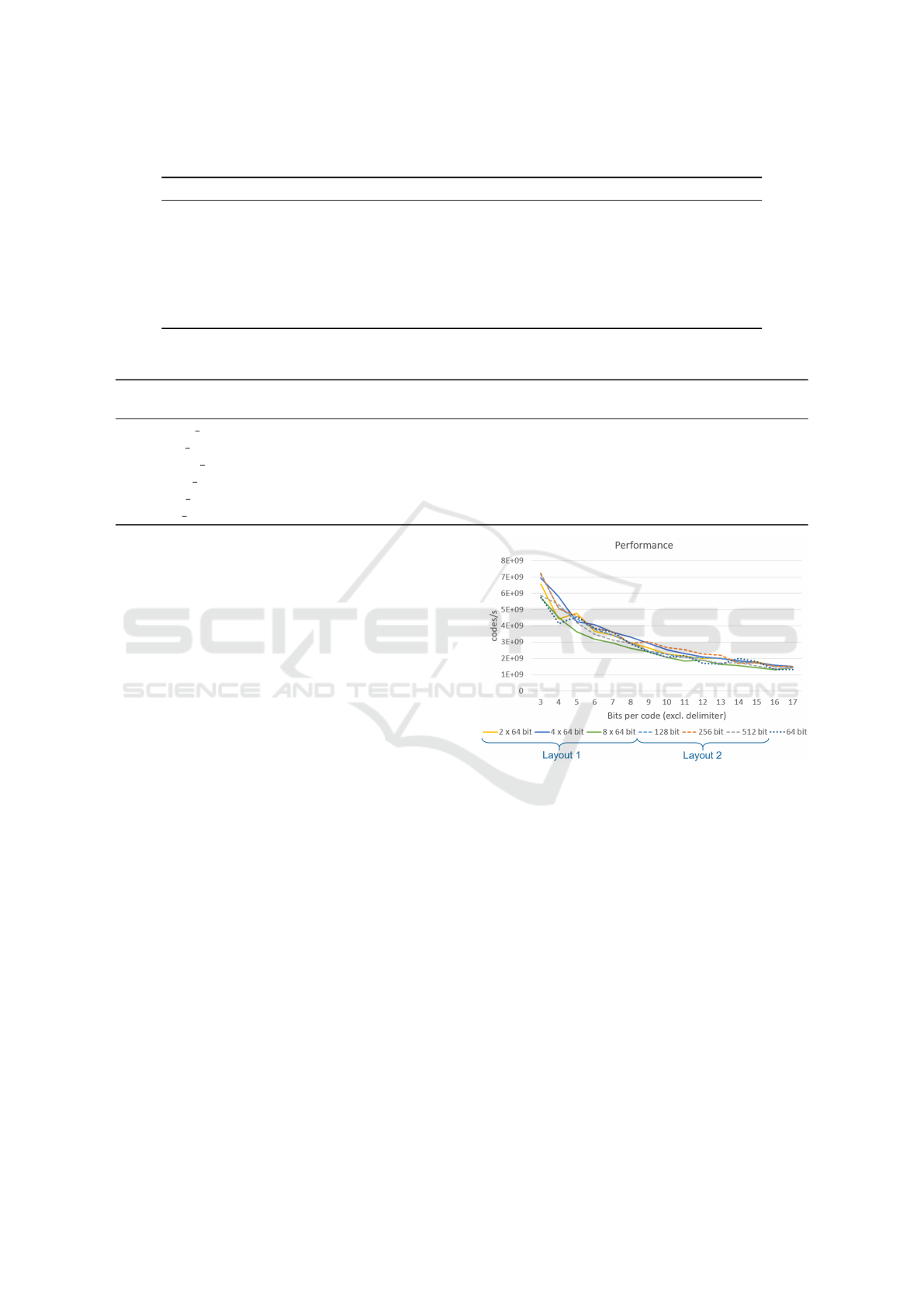
Table 1: Evaluation Results on Intel Xeon Gold 6130, 3 Bits Per Code, Average over 10 Runs.
Vector Layout Throughput(GB/s) Performance(Codes/s) Energy(Codes/J)
none (64-bit) (baseline) 2.9 57.8e+8 29.2e+6
2X64-bit (Layout 1) 3.3 65.7e+8 32e+6
4X64-bit (Layout 1) 3.5 69.3e+8 34.7e+6
8X64-bit (Layout 1) 2.9 57.6e+8 29.4e+6
128-bit (Layout 2) 3.6 71.6e+8 35.4e+6
256-bit (Layout 2) 3.6 72.4e+8 36e+6
512-bit (Layout 2) 2.9 58.9e+8 29.3e+6
Table 2: Evaluation Results for ARM-based, Basic and Hybrid Execution (3 Bits Per Code).
Hardware Throughput Performance Est. Energy Act. Energy
Design Name (GB/s) (Codes/s) (Codes/J) (Codes/J)
ARM 64 (64-bit words, Single Core) 1.9 38e+8 N/A 18e+7
ARM 256 (4X64-bit words, Quad Core) 6 120e+8 N/A 55e+7
BASIC 64 (64-bit words, Basic Arch.) 1.9 38e+8 10e+8 18e+7
BASIC 128 (128-bit words, Basic Arch.) 3.9 78e+8 20e+8 35e+7
HYBRID 512 (2X256-bit words, Hybrid Arch.) 7.7 155e+8 31e+8 67e+7
HYBRID 1024 (4X256-bit words, Hybrid Arch.) 12 240e+8 48e+8 105e+7
not the influence of multiple memory channels or
CPU cores. Thus, all benchmarks are single threaded.
For comparison, we also implemented a naive 64-bit
BitWeaving/H version without any further optimiza-
tion for special cases, such that the predicate evalua-
tion is always executed in the same way. For codes
containing 3 bits and a delimiter bit, this naive imple-
mentation achieves a throughput of 2.9 GB/s, which
equals a performance of almost 58e+8 codes per sec-
ond. Additionally, we retrieved the energy consump-
tion of all 4 power domains on the CPU and summed
them up. For this first test case with 3-bit codes and
a naive implementation (baseline), 29.2e+6 codes can
be processed with every Joule.
The results for 3-bit column codes for all different
vector layouts are shown in Table 1. All values are
averaged over 10 runs. The results show, that there
is a performance gain when using the vectorized ap-
proach, but it is not as significant as expected. For
instance, we would expect a 100% speed-up when
changing from 64 to 128 bits since we can process
twice the data at once. Unfortunately, the throughput
and the performance increase only by 14%. More-
over, it even decreases when changing from 256 to
512 bits for both vector layouts. However, these num-
bers can only provide a rough estimation since the
throughput varies by up to 0.5 GB/s between the in-
dividual runs.
Figure 9 shows the performance for all column
code sizes between 3 and 17 bits, while Figure 11
shows the energy efficiency. The differences be-
tween the vectorized implementations and the naive
implementation becomes even smaller when the code
Figure 9: Performance (SIMD-Optimization).
size increases while the throughput oscillates between
2.5 GB/s and 4 GB/s for all versions (see Figure 10).
There is a mere tendency of the 256-bit implementa-
tions to provide the best performance in average and
for the 512-bit versions to provide the least perfor-
mance. Nevertheless, the insignificance of the differ-
ences cannot be explained with the query evaluation
itself. To find the bottleneck, we deleted the evalu-
ation completely, such that only the vectorized load
and store instructions were left. Then, we measured
the throughput again and received results between
3 GB/s and 4 GB/s. A simple memcopy had a stable
performance around 4.5 GB/s. Hence, in contrast to
the naive implementation, the vectorized implemen-
tations are bound by the performance of loading and
storing data, while the peak throughput cannot be-
come larger than 4.5 GB/s. The same applies for en-
ergy efficiency. That means, the SIMD-optimization
DATA 2018 - 7th International Conference on Data Science, Technology and Applications
350
does not achieve the desired result neither from per-
formance nor from energy perspective.
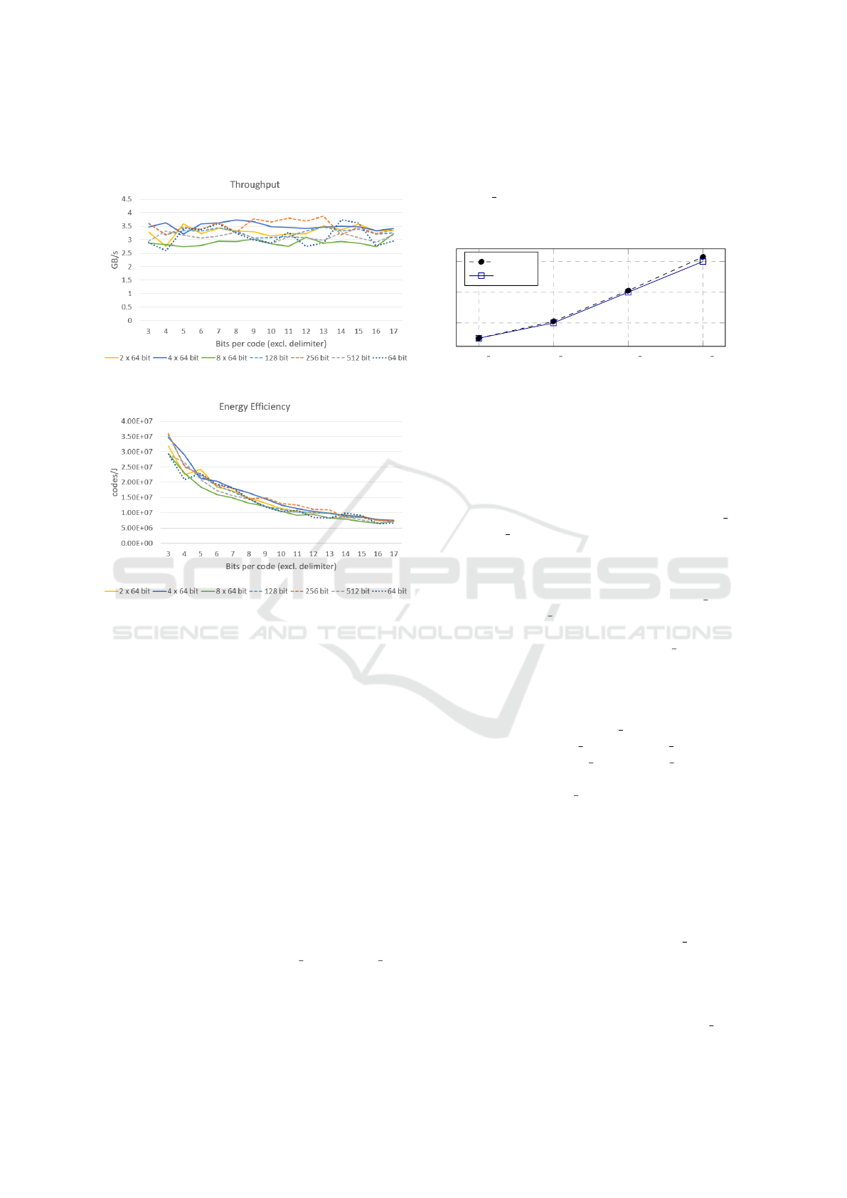
Figure 10: Throughput (SIMD-Optimization).
Figure 11: Energy Efficiency (SIMD-Optimization).
5.2 FPGA-Optimization
As done in the previous section, all designs are eval-
uated using three metrics: throughput (GB/s), perfor-
mance (Codes/s) and energy (Codes/J). Two different
ways are used for energy consumption measurement.
Firstly, we measured energy consumption using Xil-
inx® Power Tool as Estimated Energy. Secondly,
we used external power meter device as Actual En-
ergy. Actual Energy in terms of Codes/J is less than
Estimated Energy, because the Xilinx® Power Tool
estimate power consumption only for a specific cus-
tom design, whereas the power meter device measure
the real time power consumption for the entire FPGA
board.
In order to prove the efficiency of our basic and
hybrid architectures for BitWeaving/H scan, we pre-
pared also ARM-based implementations as baseline.
Therefore, we implemented single and quad ARM
cores based designs namely ARM 64 and ARM 256,
respectively, where each core is processing 64-bit
width based data words as proposed by the original
BitWeaving/H approach. We evaluated these two ap-
proaches, whereby Table 2 shows the results for 3-bit
column codes (excluding delimiter bit) with equality
check predicate during the BitWeaving/H scan. The
data words are uniformly distributed among the cores
for ARM 256 design. In addition, only Actual Energy
is measured for ARM-based designs because these
designs are not implemented using the Xilinx® tool.
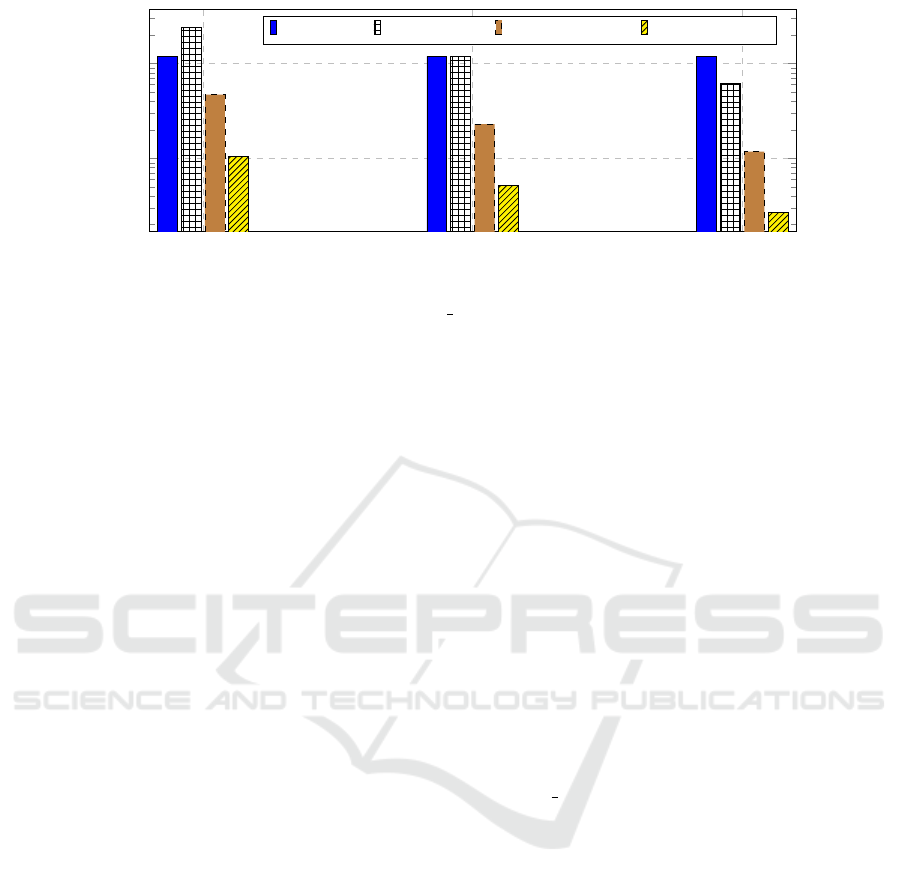
BASIC 64 BASIC 128 HYBRID 512 HYBRID 1024
2
4
6
Speedup
ECIF
Figure 12: Analysis in terms of Speedup and Energy Con-
sumption Improvement Factor (ECIF) between Basic and
Hybrid Architectures.
Afterwards, we evaluated our basic and hybrid
architectures-based designs for 3-bit column codes
(excluding delimiter bit) with equality check pred-
icate during the BitWeaving/H scan (see Table 2),
where data words are uniformly distributed among the
PEs for hybrid designs. As we can see, the ARM 64
and BASIC 64 gives the same performance, through-
put and actual energy, because in each clock cycle
both of them are processing the same width based
data words which is 64-bit and both are accessing PS
part main memory via one data channel. ARM 256 is
better than BASIC 128 for all evaluated metrics be-
cause it is processing four times of 64-bit width based
data words in parallel, whereas BASIC 128 is pro-
cessing two times of 64-bit. On the other side, the hy-
brid architecture based designs are processing beyond
256-bit width based data words through multiple main
memory data channels and also flexible to use addi-
tional hardware (i.e., Combiner 256, FIFO), which is
not available on BASIC 64 and BASIC 128 designs
and not possible on ARM 64 and ARM 256 designs
due to its non-customized hardware architecture. As a
consequence, HYBRID 1024 gives the peak through-
put of 12GB/s, whereas three data channels from PS
part main memory and one data channel from PL part
main memory are used. The behavior of all evalu-
ated metrics are identical among the basic and hybrid
designs (see Table 2). Therefore, the speedup and
the energy consumption improvement factor for main
memory-based BitWeaving/H scan among the basic
and hybrid designs on the targeted FPGA platform is
linear (see Figure 12), whereas the BASIC 64 design
is the baseline. This may lead to the conclusion, that
the hybrid architecture-based designs are very benefi-
cial for BitWeaving/H scan on FPGAs.
Finally, we evaluated different numbers of bits per
(column) code using the best design: HYBRID 1024
Column Scan Optimization by Increasing Intra-Instruction Parallelism
351
3
7
15
10
9
10
10
Bits Per Code (Excluding Delimiter Bit)
Throughput(GB/s) Performance(Codes/s) Estimated Energy(Codes/J) Actual Energy(Codes/J)
Figure 13: Analysis on HYBRID 1024 for Different Bits Per Code.
(see Figure 13). A linearly decreasing behavior found
among all metrics as the bits per code increases ex-
cept the throughput. The reason is, that the increase of
bits per code decreases the number of codes per data
word which negatively effects on those evaluated met-
rics which are evaluated on the basis of the number of
codes as expected, whereas throughput evaluation is
independent of codes.
5.3 Lesson Learned
The hardware-based optimization of BitWeaving/H
by means of SIMD or FPGA is possible. However,
the FPGA optimization is superior to SIMD optimiza-
tion from a performance as well as an energy per-
spective. Although the performance can be slightly
increased with SIMD optimization, it can not be in-
creased as much as expected. Furthermore, higher
vector widths bring no further advantages, since the
main memory bandwidth is already fully utilized for
low vector register sizes. Thus, 128-bit vector regis-
ters with a BitWeaving/H vector storage Layout 2 de-
liver the best performance on our test hardware. In
contrast to SIMD, the FPGA optimization brings a
significant increase in performance with a high en-
ergy efficiency. In this case, a data width of 1024-
bit for BitWeaving/H delivers the best performance.
Thus, FPGA optimization should be well-investigated
for database systems in the near future.
6 RELATED WORK
Generally, the efficient utilization of SIMD instruc-
tions in database systems is a very active research
field (Polychroniou et al., 2015; Zhou and Ross,
2002). On the one hand, these instructions are fre-
quently applied in lightweight data compression al-
gorithms (Damme et al., 2017; Lemire and Boytsov,
2015; Zhao et al., 2015). On the other hand, SIMD
instructions are also used in other database operations
like scans (Feng et al., 2015; Willhalm et al., 2009),
aggregations (Zhou and Ross, 2002) or joins (Balke-
sen et al., 2013).
Most research in the direction of FPGA optimiza-
tion focused on creating custom hardware modules
for different types of database query operations up to
now (Sidler et al., 2017a; Istv
´
an et al., 2017; Mueller
et al., 2009; Teubner and Woods, 2013b; Ziener et al.,
2016). For example, Ziener et al. presented con-
cepts and implementations for hardware acceleration
for almost all important operators appearing in SQL
queries (Ziener et al., 2016). Moreover, Sidler et al.
explored the benefits of specializing operators for the
Intel Xeon+FPGA machine, where the FPGA has co-
herent access to the main memory through the QPI
bus (Sidler et al., 2017a). They focused on two com-
monly used SQL operators for strings: LIKE, and
REGEXP
LIKE, and provide a novel and efficient
implementation of these operators in reconfigurable
hardware. Teubner et al. performed XML projection
on FPGAs and report on performance improvements
of several factors (Teubner, 2017).
To the best of our knowledge, none of the existing
works investigated the domain of FPGA-accelerated
data scan, whereby the scan is one of the most impor-
tant primitives in in-memory database systems.
7 CONCLUSIONS
A key primitive in in-memory column store database
systems is a column scan (Feng et al., 2015; Li and
Patel, 2013; Willhalm et al., 2009), because analyti-
cal queries usually compute aggregations over full or
large parts of columns. Thus, the optimization of the
scan primitive is very crucial (Feng et al., 2015; Li
and Patel, 2013; Willhalm et al., 2009). In this pa-
DATA 2018 - 7th International Conference on Data Science, Technology and Applications
352

per, we evaluated two hardware-based optimization
opportunities using SIMD extensions and custom ar-
chitectures on FPGA for the BitWeaving scan tech-
nique (Li and Patel, 2013). With both optimizations,
we are able to improve the scan performance, whereas
the FPGA optimization is superior to SIMD optimiza-
tion from a performance and energy perspective.
REFERENCES
Abadi, D. J., Madden, S., and Ferreira, M. (2006). Integrat-
ing compression and execution in column-oriented
database systems. In SIGMOD, pages 671–682.
Balkesen, C., Alonso, G., Teubner, J., and
¨
Ozsu, M. T.
(2013). Multi-core, main-memory joins: Sort vs. hash
revisited. PVLDB, 7(1):85–96.
Boncz, P. A., Kersten, M. L., and Manegold, S. (2008).
Breaking the memory wall in monetdb. Commun.
ACM, 51(12):77–85.
Damme, P., Habich, D., Hildebrandt, J., and Lehner, W.
(2017). Lightweight data compression algorithms: An
experimental survey (experiments and analyses). In
EDBT, pages 72–83.
Feng, Z., Lo, E., Kao, B., and Xu, W. (2015). Byteslice:
Pushing the envelop of main memory data processing
with a new storage layout. In SIGMOD, pages 31–46.
He, J., Zhang, S., and He, B. (2014). In-cache query
co-processing on coupled CPU-GPU architectures.
PVLDB, 8(4):329–340.
Hildebrandt, J., Habich, D., Damme, P., and Lehner, W.
(2016). Compression-aware in-memory query pro-
cessing: Vision, system design and beyond. In ADMS
Workshop at VLDB, pages 40–56.
Istv
´
an, Z., Sidler, D., and Alonso, G. (2017). Caribou: In-
telligent distributed storage. PVLDB, 10(11):1202–
1213.
Lemire, D. and Boytsov, L. (2015). Decoding billions of in-
tegers per second through vectorization. Softw., Pract.
Exper., 45(1).
Li, Y. and Patel, J. M. (2013). Bitweaving: Fast scans for
main memory data processing. In SIGMOD, pages
289–300.
Mueller, R., Teubner, J., and Alonso, G. (2009). Data pro-
cessing on fpgas. Proc. VLDB Endow., 2(1):910–921.
Oukid, I., Booss, D., Lespinasse, A., Lehner, W., Willhalm,
T., and Gomes, G. (2017). Memory management tech-
niques for large-scale persistent-main-memory sys-
tems. PVLDB, 10(11):1166–1177.
Polychroniou, O., Raghavan, A., and Ross, K. A.
(2015). Rethinking SIMD vectorization for in-
memory databases. In SIGMOD, pages 1493–1508.
Sidler, D., Istv
´
an, Z., Owaida, M., and Alonso, G. (2017a).
Accelerating pattern matching queries in hybrid CPU-
FPGA architectures. In SIGMOD, pages 403–415.
Sidler, D., Istvan, Z., Owaida, M., Kara, K., and Alonso, G.
(2017b). doppiodb: A hardware accelerated database.
In SIGMOD, pages 1659–1662.
Stonebraker, M., Abadi, D. J., Batkin, A., Chen, X., Cher-
niack, M., Ferreira, M., Lau, E., Lin, A., Madden,
S., O’Neil, E. J., O’Neil, P. E., Rasin, A., Tran, N.,
and Zdonik, S. B. (2005). C-store: A column-oriented
DBMS. In VLDB, pages 553–564.
Teubner, J. (2017). Fpgas for data processing: Current state.
it - Information Technology, 59(3):125.
Teubner, J. and Woods, L. (2013a). Data Processing on FP-
GAs. Synthesis Lectures on Data Management. Mor-
gan & Claypool Publishers.
Teubner, J. and Woods, L. (2013b). Data Processing on FP-
GAs. Synthesis Lectures on Data Management. Mor-
gan & Claypool Publishers.
Willhalm, T., Popovici, N., Boshmaf, Y., Plattner, H., Zeier,
A., and Schaffner, J. (2009). Simd-scan: Ultra fast
in-memory table scan using on-chip vector processing
units. VLDB, 2(1):385–394.
Xilinx (2017). Zynq UltraScale+ MPSoC Data Sheet:
Overview.
Zhao, W. X., Zhang, X., Lemire, D., Shan, D., Nie, J., Yan,
H., and Wen, J. (2015). A general simd-based ap-
proach to accelerating compression algorithms. ACM
Trans. Inf. Syst., 33(3).
Zhou, J. and Ross, K. A. (2002). Implementing database op-
erations using SIMD instructions. In SIGMOD, pages
145–156.
Ziener, D., Bauer, F., Becher, A., Dennl, C., Meyer-
Wegener, K., Sch
¨
urfeld, U., Teich, J., Vogt, J.-S., and
Weber, H. (2016). Fpga-based dynamically reconfig-
urable sql query processing. ACM Trans. Reconfig-
urable Technol. Syst., 9(4):25:1–25:24.
Zukowski, M., H
´
eman, S., Nes, N., and Boncz, P. A.
(2006). Super-scalar RAM-CPU cache compression.
In ICDE, page 59.
Column Scan Optimization by Increasing Intra-Instruction Parallelism
353
