
Design of Pulse Power Supply Voltage Acquisition and Adjustment
S
y
stem Based on AD7888
Qing Wang, Yongbin Zhang, Jinming Chen, Guangmin Liu and Feng Wang
Institute of Mechanical Manufacturing Technology, China Academy of Engineering Physics, Mianyang, Sichuan, China
chenjmcaep@sina.com
Keywords: Pulse power supply, AD7888, SPI bus, Voltage acquisition, Voltage feedback adjustment.
Abstract: The precision of the output current of the pulse power applied to precision electroplating is an important factor
that affects the quality of the plating. To accurately control the current requires precision acquisition of the
power voltage in real-time. This paper introduces the hardware interface and the implementation procedures of
the voltage acquisition module in detail. In the voltage acquisition module, FPGA is the main controller and
the AD7888 is an analog to digital converter (ADC). They are linked by the SPI bus. The program is based on
the timing of AD7888 interface. It can realize the SPI bus serial communication between FPGA and AD7888
and take up fewer resources. Based on the real-time acquisition voltage of AD7888, we choose the proper duty
cycle step size in different voltage intervals by fitting the power characteristic curve, so as to achieve fast and
accurate adjustment of the pulse power supply voltage.
1 INTRODUCTION
Electroplating is a technique commonly used to im-
prove the appearance and surface properties of the
workpiece. Pulse electroplating can obviously im-
prove the quality of the coating by using pulse cur-
rent. Pulse electroplating power is a device to produce
pulse waveform, and the stability of its output current
is an important factor that affecting the quality of the
electroplating layer. In general, the current is pre-
cisely controlled by monitoring the current value in
real-time. During the commissioning of the pulse
power supply, the voltage at both ends of capacitor is
used as reference voltage, and the voltage’s stability
is much higher than that of current. By collecting
voltage value in real time, the error of data acquisition
can be reduced obviously. When the circuit compo-
nents are determined, there is a fixed function rela-
tionship between the voltage and the current. There-
fore, in this paper, a suitable ADC is selected and the
SPI bus is utilized to connect the ADC with the main
controller to realize the real-time acquisition of volt-
age equivalent. Collected voltage equivalent data are
used as the reference value of the control voltage, and
the reference value of the voltage is compared with
the set value, and the precise control of voltage can be
realized through closed loop feedback adjustment.
2 INTERFACE DESIGN BE-
TWEEN FPGA AND AD7888
2.1 System Construction
The system structure is given in Figure 1. The field
programmable gate array (FPGA) is configured flex-
ibly and is used as the main controller. Functional
modules in FPGA include voltage sampling pro-
cessing unit, forward pulse control unit and voltage
adjustment unit. In the voltage sampling processing
unit, the real-time monitoring of the voltage is real-
ized by the ADC. The selection of AD Chips should
take the speed, precision, power, cost and installation
of the system into account. AD7888 is a 12 bit 8 chan-
nels ADC with the minimum and the lowest power
consumption. The voltage adjustment in the voltage
regulating unit is realized by controlling the
MOSFET Q
1
on and off. The forward pulse control
unit is used to generate the forward pulse waveform,
changing the break time of Q
2
can output pulse wave-
form with different duty cycle.
510
Wang, Q., Zhang, Y., Chen, J., Liu, G. and Wang, F.
Design of Pulse Power Supply Voltage Acquisition and Adjustment System Based on AD7888.
In 3rd International Conference on Electromechanical Control Technology and Transportation (ICECTT 2018), pages 510-517
ISBN: 978-989-758-312-4
Copyright © 2018 by SCITEPRESS – Science and Technology Publications, Lda. All rights reserved
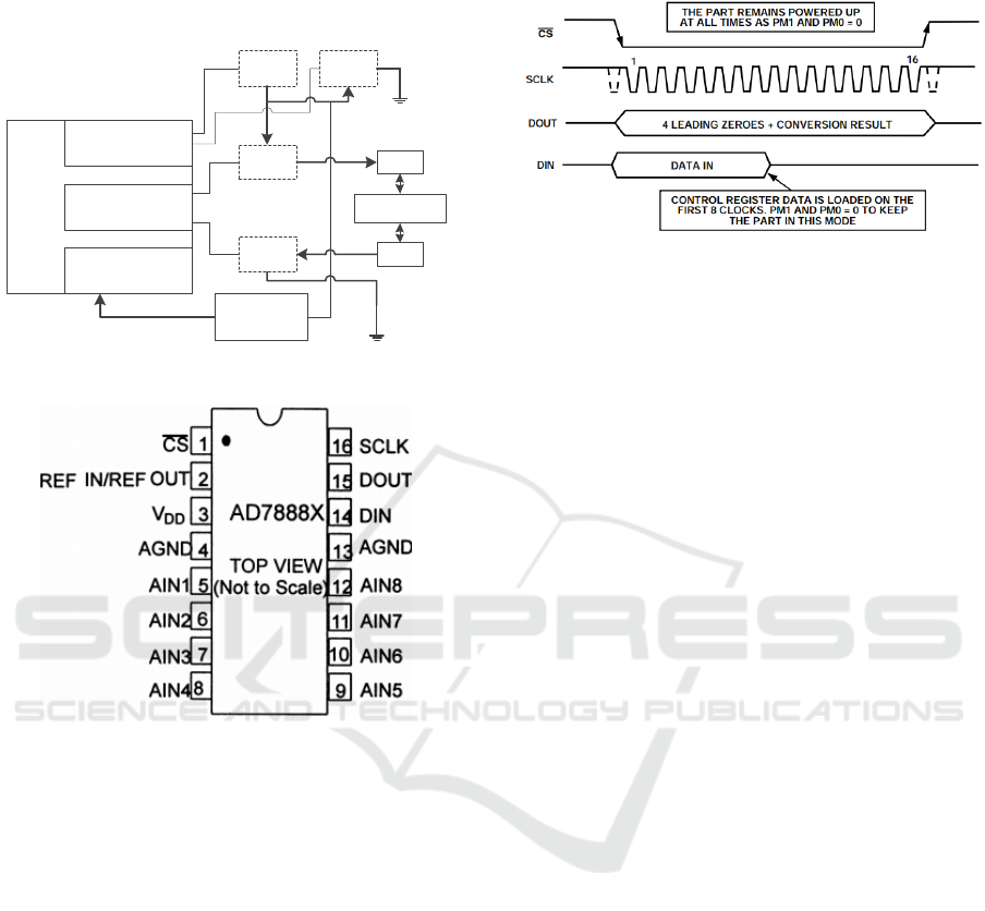
AD7888's pin configurations are illustrated in
Figure 2. AD7888 uses a single power supply, work-
ing from 2.7V to 5.25V, and its maximum pass rate is
125kSPS.
Figure 1: The system structure.
Figure 2: AD7888’s pin configurations.
Its control words are introduced from the DIN pin
to the 8 - bit, only written control register on the rising
edge of the control clock (CLK). The serial interface
timing diagram of AD7888 is illustrated in Figure 3.
The completion of a digital conversion requires 16 se-
rial clock cycles, in which the control word is input to
the control register on the rising edge of the first 8
clock pulses. The converted data are output bit by bit
by the DOUT pin while the conversion results are
read out. When using the chip, the chip select signal
should be at least 10 ns earlier than the falling edge of
SCLK, serial data after the analog-digital conversion
should be output by DOUT within 100ns.
The SPI bus is a serial interface commonly used
in AD7888, which has the characteristics of little con-
nection and good independence. A typical SPI bus
consists of a serial clock line (SCLK), a master output
/ slave input line (MISO) and a master input / slave
output line (MISO) and a slave select line (SS). All of
the data transfers are synchronized with the serial
clock, and the transmission of 1Bit data requires a
clock pulse.
Figure 3: Serial Interface Timing Diagram of
AD7888.
The control time series of SPI bus can be realized
by FPGA through Verilog language programming.
The standard SPI bus IP core occupies more on-
chip resources. This design uses a simple method to
simulate the analog SPI interface between FPGA and
AD7888 by programming.
2.2 FPGA and AD7888 Verilog Interface
Description
In order to guarantee the normal operation of
AD7888, a periodic square wave should be input as a
chip select signal at the / CS pin. The control clock is
input from the CLK pin. The control word is written
into the control register within AD7888 through DIN.
The AD converted 12-bit data are output from DOUT
to the FPGA's internal registers. According to the
above requirements, the SPI bus interface module
consists of four parts, including the clock generation
module, the data input register, the control state ma-
chine and the shift register. The clock generation
module divides the 50 MHz clock provided in the sys-
tem to get the working clock CLK of the AD7888.
The control register's reference clock is CLK. The
control state machine controls the shift operation of
the input / output shift register and generates the chip
select signal / CS. The data in the input shift register
is output by DIN. Data output via DOUT is stored in
the output register through the output shift register.
They combine into a complete 12-bit data. Figure 4 is
the interface structure between the SPI bus and
AD7888.
The interface program is based on the working se-
quence and principle of the AD7888. The working
clock of AD7888 should take into account the number
of acquisitions of voltage value and the speed of ac-
quisition. AD7888 work at full power and uses inter-
nal benchmarks to collect data from the AIN1 channel.
According to the above setting, the control word put
voltage
adjustment unit
voltage sampling
processing unit
AD7888
Sampling Circuit
12Bit
Q1
MOSFET
Q2
MOSFET
forward pulse
control unit
Q6
MOSFET
Q5
MOSFET
Anode
Cathod
10ohm
resistent
PWM Boost
PWM Depressurization
FPGA
System
Module
Design of Pulse Power Supply Voltage Acquisition and Adjustment System Based on AD7888
511

into AD7888 is 8'b0. The program flow chart is given
in Figure 5. Figure 6 is an interface module that is
compiled by the program.
Figure 4: The interface structure between SPI bus
and AD7888.
When starting to collect the voltage value, the
chip select signal of AD7888 changes from high level
to low level.
parameter[7:0]Control_Register=8'b0;
//DOONTC/ZER0/ADD2/ADD1/ADD0/REF/PM1/PM2
always@(posedge clk1M)
begin
case(cnt2)
17'd0 : begin
ad_cs_n <= 1'b1;
ad_clk <= 1'b1;
ad_din <= 1'b0;
adc_temp_data <=12'b0;
end
17'd1 : begin
ad_cs_n <=1'b0;//start
ad_clk <= 1'b1;
ad_din <= 1'b0;
end
17'd2 : begin
ad_cs_n <= 1'b0;
ad_clk <= 1'b0;
ad_din<=Control_Register[7];
//write Control_Register
end
17'd3 : begin
ad_cs_n <= 1'b0;
ad_clk <= 1'b1;
// the first rising_edge clk
ad_din<=Control_Register[7];
end
Other control words are written to the control reg-
ister in the same way from high to low.
17'd10 : begin
ad_cs_n <= 1'b0;
ad_clk <= 1'b0;
ad_din <= Control_Register[3];
end
17'd11 : begin
ad_cs_n <= 1'b0;
ad_clk <= 1'b1;
//5 rising_edge clk
ad_din <= Control_Register[3];
adc_temp_data[11] <=ad_dout;
end
17'd12 : begin
ad_cs_n <= 1'b0;
ad_clk <= 1'b0;
ad_din <= Control_Register[2];
adc_temp_data<= adc_temp_data;
end
17'd13 : begin
ad_cs_n <= 1'b0;
ad_clk <= 1'b1;
//6 rising_edge clk
ad_din <= Control_Register[2];
adc_temp_data[10] <=ad_dout;
end
The data after the analog digital conversion is out-
put at the rising edge of each synchronous clock and
is locked at the drop edge of the clock.
17'd33 : begin
ad_cs_n <= 1'b0;
ad_clk <= 1'b1;
//16 rising_edge clk
adc_temp_data[0] <=ad_dout;
end
After completing a data acquisition, the chip se-
lect signal is set to high.
17'd34 :begin
ad_cs_n <= 1'b1;
ad_clk <= 1'b1;//over
adc_temp_data <= adc_temp_data;
adc_data_r<=adc_data_r+adc_temp_data;
if(cnt3== 5'd29)
begin
adc_data<=adc_data_r/30;
adc_data_r <= 16'b0;
end
else
adc_data <= adc_data;
end
Define a counter to count the data collected by
AD7888. If the value of the counter reaches 29, the
current accumulative value is divided by 30 to get the
average value of the voltage. Utilizing the above
treatment can significantly reduce the voltage acqui-
sition error.
CS
CLK
DOUT
DIN
AD7888
Clock
Generation
Module
Control State
Machine
output register
Input Shift Register
output Shift Register
shift Register
SPI
BUS
Input
register
ICECTT 2018 - 3rd International Conference on Electromechanical Control Technology and Transportation
512
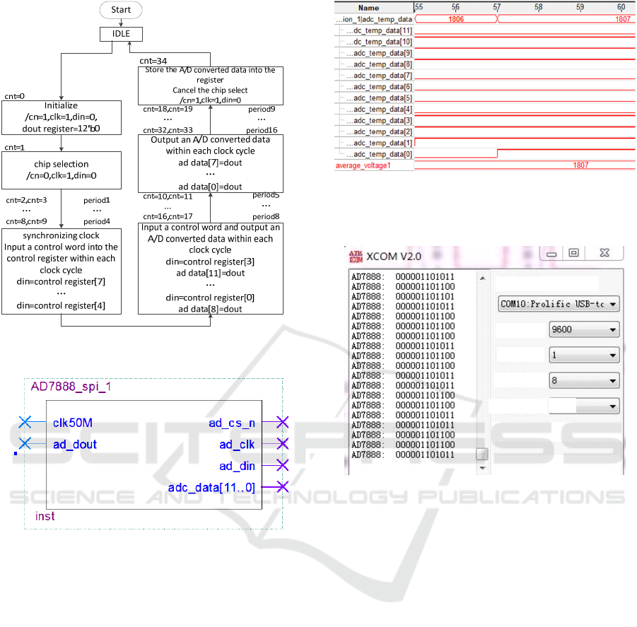
Figure 5: The program flow chart.
Figure 6: AD7888-SPI interface module.
2.3 Simulation and Verification
When the occupied space is relatively small, the data
of AD7888 is collected by signaltap. Otherwise, use
the serial port assistant to collect the voltage signal.
Signaltap can capture and display real-time signals.
In Figure 7, both real-time data and average data over
30 acquisitions acquired from AD7888 can be ob-
served. Serial port assistant can receive the binary
data that FPGA outputs after connecting with FPGA
through RS-232. The results are shown in Figure 8.
The duty cycle of Q1 is set to 7500 and the voltage
equivalent value of the AD7888 is converted to 107
or 108 in decimal.
Figure 7: Real-time data and average data required
from AD7888.
Serial port selection
Baud rate
Stop bit
Data bit
Parity check
NO
Figure 8: The serial port assistant required binary
data from AD7888.
Signaltap and Serial Assistant show the AD7888
analog to digital conversion of the average voltage
value, and the design of the circuit voltage is expected,
the functional simulation results are correct.
3 VOLTAGE ADJUSTMENT
MODULE DESIGN
The main function of the voltage adjustment module
is to make the pulse power supply accurately and
quickly output the target voltage. Figure 9 shows the
power supply voltage adjustment and measurement
principle. The voltage across capacitor P
2
can be
modified by adjusting the duty cycle of MOSFET Q
1
.
The cycle / pulse width is used to represent the duty
cycle in this article's programming and experimenta-
tion. In the power test stage, when Q
1
's duty cycle x
is constant, the actual voltage V
act
of the capacitor P
2
can be measured by a multimeter, and the voltage
equivalent V
equ
at the current duty cycle x can be
Design of Pulse Power Supply Voltage Acquisition and Adjustment System Based on AD7888
513

monitored using the AD7888. Based on the above
measurements, two functional relationships between
the V
equ
and V
act
, x and V
act
can be established. Based
on these two functional relationships, the voltage
across P
2
can be adjusted to the error of the set voltage
by adjusting the duty cycle of Q
1
.
Figure 9: the power supply voltage adjustment and
measurement principle.
3.1 Pulse Power Experiment and Data
Processing
In the pulse power experiment, the pulse width of the
output pulse waveform is 50 μs and the duty cycle is
10. The pulse width of Q
1
is 1 μs, and its duty ratio
varies between 1~10000. Some of the experimental
data are given in Table 1. The obtained experimental
data are fitted with origin for function fitting. The
point corresponding to the voltage equivalent V
equ
and the actual voltage V
act
value are depicted in the
coordinate system. It can be observed that the func-
tional relations between them are approximately lin-
ear and have insignificant inflection points. Therefore,
linear and piecewise linear fitting function relations
are chosen respectively. The formula of function re-
lation obtained by linear fitting is
y=a+b*x
(1)
The formula of function relation obtained by
piecewise linear fitting is
x<xi, y=a1+k1*x
(2)
x>xi, y=a2+k2*x
(3)
The results obtained are shown in Figure 10. The
difference between the fitting value and the actual
value obtained by the two fitting methods is shown in
Figure 11.
In Figure 10, the fitting result of (a) is
y=-94.995+3.364x
(4)
The fitting result of (b) is
y=-1468.854+4.192x
(5)
Table 1 Experimental data
Serial
Number
Duty cycle
Q1
V
equ
P2 Vact(mv)
1 1 1886 6480
2 5 1867 6380
3 15 1837 6230
4 25 1801 6060
5 35 1771 5940
6 40 1759 5870
7 35 1771 5940
8 75 1673 5510
9 100 1611 5270
10 135 1538 5000
11 170 1465 4750
12 300 1251 4000
13 400 1126 3600
14 520 1001 3200
15 680 875 2800
16 840 780 2500
17 2000 446 1400
18 2900 326 1040
19 5000 212 698
20 9000 127 408
The function is segmented when the V
equ
of P
2
is
1507. Figure 11 shows the difference between fitted
values obtained by two methods and actual values.
The fitted values obtained by the piecewise linear fit-
ting method is far less than those obtained by the lin-
ear fitting method. Therefore, piecewise linear fitting
is applied to the voltage adjustment module. In the
experiment, the pulse width of Q
1
, Q
2
and the Q
2
duty
cycle remain unchanged, Q
1
’s duty cycle changes
from 1~10000, the voltage equivalent value collected
by AD7888 can be converted to the actual voltage
value by this function relation. Figure 12 shows the
fitting results between Q1’s duty cycle and V
act
,
y=10^5/(15.783+0.0295x)
(6)
ICECTT 2018 - 3rd International Conference on Electromechanical Control Technology and Transportation
514
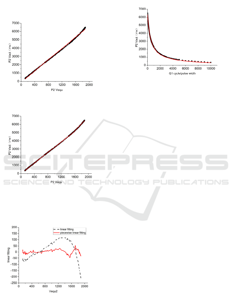
The function relation between them is approxi-
mately inverse proportionate.
(a)
(b)
Figure 10 (a)Linear Fitting of Experimental Data
(b)Piecewise Linear Fitting of Experimental Data
Figure 11: The difference between the fitting value and the
actual value by the two fitting methods.
Figure 12: The fitting results between Q1’s duty cycle and
Vact.
3.2 The Principle of Voltage Adjustment
and Its Verilog Implementation
Voltage adjustment is based on feedback adjustment.
The method of voltage adjustment is to select the suit-
able duty cycle step length in different voltage inter-
vals. When the setting voltage is V
set
, the principle of
voltage adjustment is based on the functional relation-
ship between V
equ
and V
act
, and the functional rela-
tionship between x(the duty cycle of Q
1
) and V
act
. To
make the power supply output to the set voltage,
firstly, an approximate value x
0
of x is determined as
an initial value by the function of the x and V
act
(The
error of this function is larger). x changes in certain
steps, at the same time, use the AD7888 to monitor
the voltage obtained at the corresponding value of x.
Secondly, convert V
equ
into V
act
through the func-
tional relationship between V
equ
and V
act
. Thirdly,
compare V
act
with V
set
. When | V
act
-V
set
| <20mV,
keeps the value of x unchanged and output the voltage
corresponding to x.
Based on the above principle, the voltage adjust-
ment process is optimized to enable the power supply
to output the set voltage accurately and quickly. Ob-
viously, the function between x and V
act
is similar to
the inverse proportion. In the range of V
act
>6V, to
prevent the occurrence of x<0 in the calculation, the
interval above 6V in this functional relationship is ap-
proximately treated as a linear relationship. The func-
tion relations in other intervals remain unchanged. In
order to obtain the initial duty cycle x0 closer to the
exact value. From the function relation of x and V
act
,
when V
act
is greater than 5V, V
act
varies by more than
30mV each time the value of x is changed by 1. If the
step length of x is kept at 1, this will make the voltage
fail to reach the set value. If the step length of x is too
small, the voltage adjustment process will be slow.
Therefore, different steps are selected in different
Design of Pulse Power Supply Voltage Acquisition and Adjustment System Based on AD7888
515
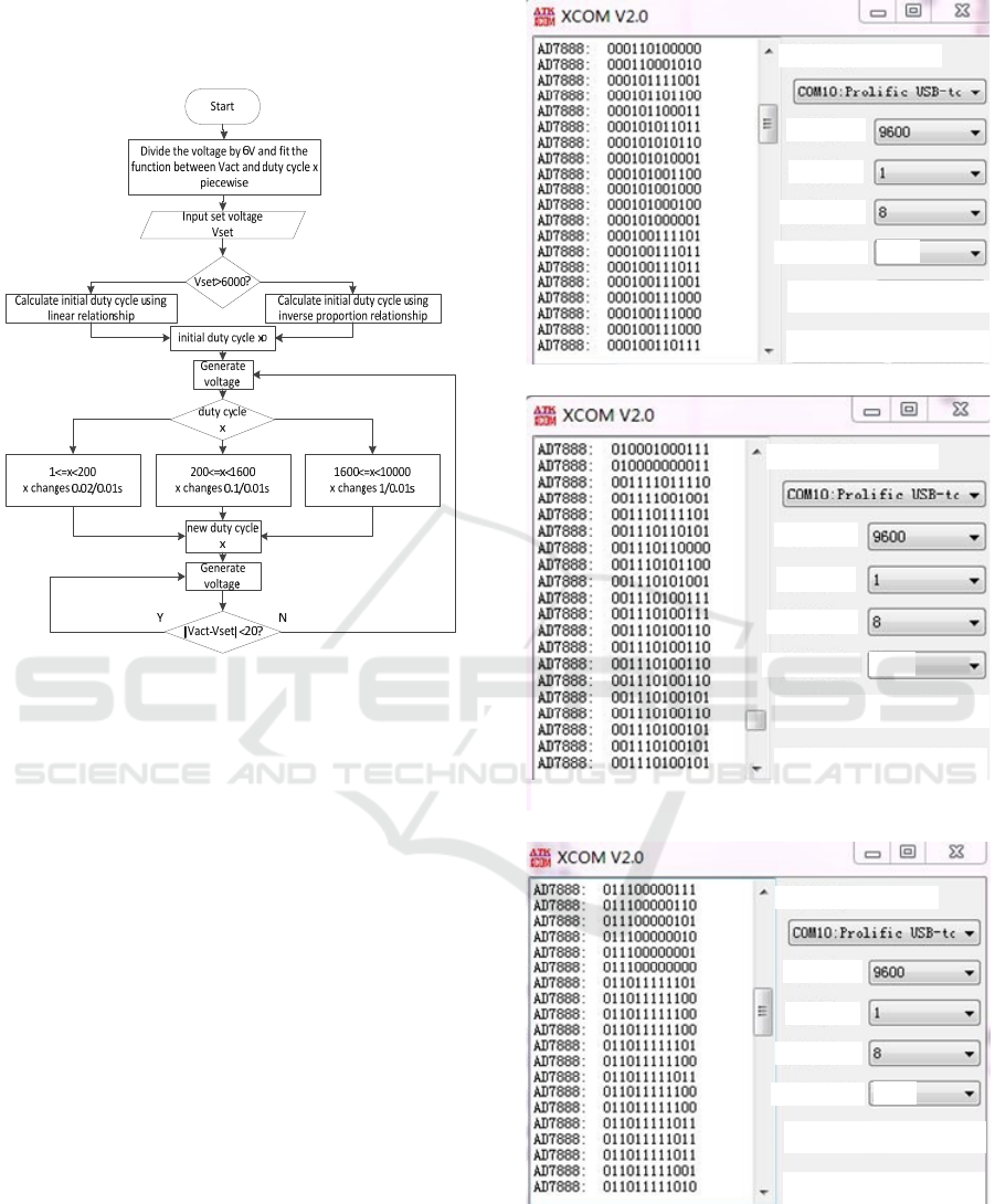
range of x values to meet the needs of the power sup-
ply for accurate and rapid voltage adjustment. Volt-
age adjustment flow is shown in Figure 13.
Figure 13: The voltage adjustment flow.
3.3 Experimental Result
In the voltage adjustment experiment, the voltage val-
ues are set to 1V, 3V and 6V, respectively. Using a
serial port assistant to receive real-time voltage equiv-
alent values in the voltage adjustment process col-
lected by AD7888. The results are given in Figure 14.
When the data is received at the 9600 baud rate, the
voltage equivalent value can be stabilized within 15
sets of data. Therefore, when the error range of volt-
age adjustment is set within 30mV, the voltage ad-
justment module can be used to output an accurate
and stable voltage within 10s.
Serial port selection
Baud rate
Stop bit
Data bit
Parity check
NO
(a)
Serial port selection
Baud rate
Stop bit
Data bit
Parity check
NO
(b)
Serial port selection
Baud rate
Stop bit
Data bit
Parity check
NO
(c)
Figure 14: Voltage adjustment results received by serial
port assistant. (a)Vset is 1V, (b)Vset is 3V, (c)Vset is 6V.
ICECTT 2018 - 3rd International Conference on Electromechanical Control Technology and Transportation
516

4 CONCLUSIONS
This paper introduces a kind of SPI bus interface de-
sign, which takes the FPGA as the main controller,
the AD7888 as the ADC. The serial communication
between FPGA and AD7888 is realized by program-
ming. Real-time voltage monitoring data for pulse
electroplating power supply can be obtained by sig-
naltap or serial port assistant. The program occupies
less FPGA on-chip resources. On the basis of real-
time monitoring of supply voltage, the method of ad-
justing the voltage is Choose different duty cycle
steps in different voltage intervals. The voltage is set
to approach the set voltage by calculating the initial
duty cycle. The duty cycle value is then changed by
closed-loop feedback. This causes the pulse power
supply to output the desired voltage. The experi-
mental results show that the voltage equivalent value
collected by AD7888 is in accordance with the actual
voltage. The voltage adjustment is accurate and fast,
it meets the requirements of the use of pulse power
supply, and the reliability is high.
ACKNOWLEDGEMENTS
The authors appreciate the support from the National
Natural Science Foundation of China (Grant No.
51475439) and Sichuan Provincial Science and Tech-
nology Department of application-based projects
(Grant No. 2016JY0109).
REFERENCES
Kewang Zheng, Daibo Xing, Tenguan Ding. Design of volt-
age acquisition module based on FPGA in network ac-
quisition system [J]. China Science and Technology
Information, 2017, (10): 75-77.
Gang JIN, Zhong CHEN, Yue HONG. Application of Syn-
chronous Serial SPI in AD7888 and AT90S8515 Inter-
face [J]. Microcomputer Information, 2004, (02): 91-
92.
Jian-ze WANG, Yu-ming PEI, Jia YANG. Application of
Analog to Digital Converter AD7888 [J] .Journal of Ji-
lin University of Architecture& Civil Engineering,
2010, 27 (4): 53-56.
Tao Geng, Guochao Li, Bingqiang Li ,Ying Gao.Design
and Implementation of Analog-to-Digital Converter
AD7888 Interface Based on FPGA [J] .Journal of In-
formation and Computers (Theory Version), 2014 (04):
31-33
.
Chunqing Xuan. Design and implementation of embedded
portable measuring instrument based on AD7888
[J] .Chinese Journal of Nuclear Electronics and Detec-
tion, 2014,34 (05): 598-601.
Zhen Wang, Ludan Li. Design of Airborne 270V DC Mon-
itoring System Based on AD7888 Chip
[J] .Infor-
mation Systems Engineering, 2017 (09): 126-127 +
129.
Design of Pulse Power Supply Voltage Acquisition and Adjustment System Based on AD7888
517
