
Thermal Optimization Design of PBGA Package Based on
Finite Element Analysis
Hui Yang
1
,Jihui Wu
1
and Yang Zhang
1
1
College of Mechanical and Control Engineering
,
Guilin University of Technology,Yanshan District,Guilin,China
Keywords: Tlectronic packaging, heat dissipation structure, inite element, optimization design.
Abstract: In order to solve the problem of chip heat dissipation in PBGA package, this paper takes PBGA as the
research Object to study the reliability of electronic packaging. Since the BGA package form is the main
packaging technology at present, the problem of thermal failure has been particularly prominent in BGA,
which also became the hot issues^([1]). Now a method is proposed to establish a finite element
approximation model of the package structure, perform thermal stress analysis, and reconstruct the original
optimization problem. Identify the influencing factors of thermal failure, and based on these problems,
through the establishment of mathematical model analysis, optimize the structure. And for problems that
can not be fully solved by the stablilization, the key points of future research directions are proposed and the
next step of research work is guided.
1 INTRODUCTION
At present, one of the most important failure forms
of electronic devices is thermal failure. According to
relevant statistics, due to the high temperature, the
proportion of electronic equipment failures is as high
as 55%, and from a quantitative point of view, with
increasing temperature, the failure rate will show
exponential growth, for most electronic devices,
Even lowering the temperature to a very small value
will greatly reduce the chance of its equipment
failure. It can be seen that how important the thermal
design of electronic equipment is, and that it will
receive more and more attention[2].Therefore, using
a reasonable thermal design to improve heat
dissipation is one of the key technologies to ensure
the overall reliability of electronic products.
2. TWO-DIMENSIONAL MODEL
ANALYSIS
The most common BGA package type PBGA, as
shown in Figure 2.1. The PGBA carrier or interposer
is a common printed board substrate. The chip is
connected to the upper surface of the carrier by wire
bonding, then injection moding is performed using a
plastic model, and an array of solder balls containing
the alloy components is connected to the lower
surface of the carrier[3].The array of solder balls can
appear completely or partially distributed on the
bottom surface of the device. Generally, The
diameter of the solder ball is in the range of
0.75mm-0.89mm, and the center distance of the
solder ball is 0.8mm, 1.0mm, 1.27mm, 1.5mm, etc.
The minimum is 0.5mm.
Fig.2.1 PBGA structural model diagram.
In the model, the plastic package, the chip, the
adhesive, the substrate, the board, the copper traces,
and the solder joints under the substrate constitute a
seven-layer structure that does not consider the
influence of other fine structures such as bond
wires[4-6].The purpose is to avoid the analysis.
Handle complex structures. In addition to the solder
joints, the six-layer material in the model structure is
considered to be an isotropic and evenly distributed
material. The characteristic parameters of the
material use the characteristic parameters of the
main material of each layer, as shown in Table 2.1.
Tab.2.1 Material characteristics table.
3. FINITE ELEMENT MODEL
Based on the two-dimensional model, the PBGA
three-dimensional model was established on
ANSYS. Because the package is a symmetrical
structure, a quarter structure is used here for
analysis. Using three-dimensional 10-node
tetrahedral elements for meshing, there are 30485
finite elements, there are 56432 nodes.
Fig.3.1 Meshing
Thermal cycling and heat generation analysis
considering the actual working conditions of the
package.
In the actual operation of PBGA, there will be a
stable energy applied to the chip layer. We assume
that the value is 2W. After applying energy under
normal operating conditions, a temperature
distribution will be generated in the package and it
will be a heating. The process of warming up. Now
suppose that the temperature gradient still remains in
the ambient temperature change, that is, the thermal
cycle, so the temperature distribution has an initial
temperature distribution and the resulting initial
stress before the temperature distribution increases
from room temperature 20°C to 105°C to 125°C[7-
8]Then in this way, the value of each parameter
obtained by numerical simulation will change in the
subsequent thermal cycle. Also from the thermal
deformation of the PBGA package, the equivalent
stress at the chip, and the thermal fatigue life of the
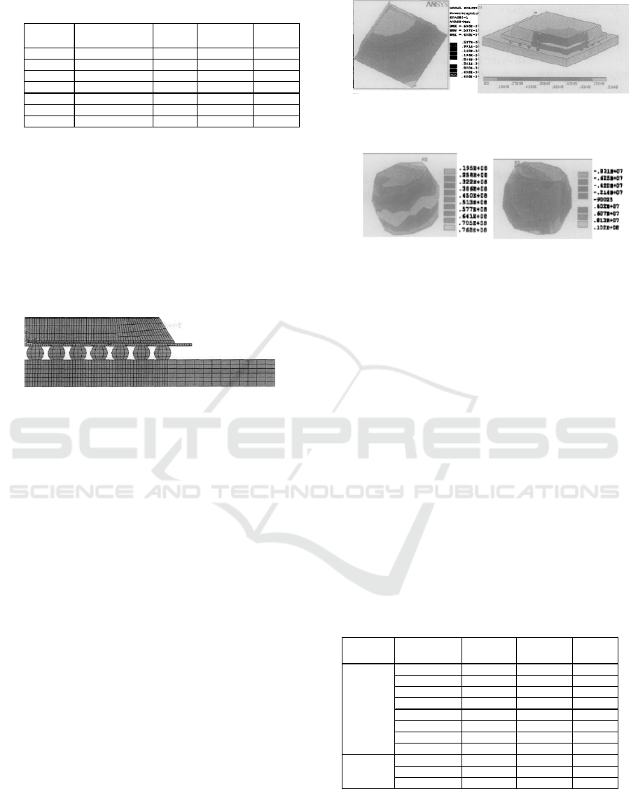
solder joint, as shown in Figure 3.2, 3.3,3.4.
Fig.3.2 Deformation Fig.3.3 von Mises Stress distribution.
Picture of PBGA Package.
Fig.3.4 Stress distribution map of key solder joints.
4.OPTIMUM DESIGN OF PBGA
PACKAGE
The optimal design of the package is to optimize the
thickness and material of each device under the
constraints of its stiffness, strength and thermal
deformation to reduce the maximum stress of the
package and enhance its reliability. However,
considering the numerical simulation analysis of the
thermal-structure of the packaged integrated circuit
chip package and the practical application of the
optimized design body, the structural self-weight
must be appropriately limited to ensure the actual
weight. Therefore, in this paper, two optimization
schemes are adopted for this situation: one is to
minimize the weight of the structure as the objective
function; the other is to minimize the maximum
stress as the objective function.
Tab.4.1 The parameters of model components material.
Mode l parts Mate rial ingredient
Elastic
Modulus
Poisson's ratio
Co e fficie nt
of expans ion
Solde r ball
63Sn37Pb 14.7 0.3 2.10E-05
PCB board
FR -4 22 0.28 1.80E-05
Subs trate
P olyimide 22 0. 28 1. 80E-05
Printed line
coppe
r
120.658 0.345 1.70E-04
Binder
Epoxy resi
n
5.2 0.3 40.0E -6
Chip
silicon 131 0.3 2.80E-06
Plas tic s e al
Resi
n
26 0.3 7.00E-06
Mate rial name Mate rial coding
El a s t i c
Modu lu s(G pa)
Coefficient of
the rmal
expansion
Poisson
rati o
A 12.4 11.6 0.3
B 12.3 12 0.3
C 11.3 12.2 0.3
D 11.8 14.2 0.3
E 12.5 12.7 0.3
F 13.8 13.2 0.3
G 14.2 13.8 0.3
H 14.7 14.5 0.3
a 0.893 55 0.35
b 1.405 45 0.21
c 2 40 0.3
Binder
Packaging
materials

5. OPTIMIZATION
The objective function is to minimize the maximum
stress on the package. Optimizing the design
variables is the choice of the thickness of each
device and the material[9.]The state variables are
considered as follows: 1.The maximum temperature
of the package after heat generation to ensure that
the initial temperature and initial stress distribution
are not large before the thermal cycle; 2. The
deformation of the package to meet the structural
rigidity requirements. 3 The weight of the entire
package to ensure that the weight of the structure
changes within a certain range, with good
application. Writing a mathematical model is as
follows: Design variable:
T
,
,
,
⋯,
t refers to the thickness of
each device
The objective function:
min
max(T)
(T) (k1,2,⋯,
)
Restrictions:
1,2,⋯
σ,w denotes stress and deformation; j,k denotes
the number of stress and deformation variables.
Tab.4.3 he result with Chip Thiekness
From the data in Table 3.2, it can be seen that,
except for the data of the temperature gradient
column, the other data is almost the same as the
trend of the data in the scenario 1. Only the effect of
stress and heat distortion is slightly different. The
greater the thickness of the chip, the smaller the
temperature gradient generated by the heat
dissipation power
. This is due to the increase
in the thickness of the chip, the volume of which
also increases, and the heat generation per unit
volume is inversely proportional to the volume, that
is, the larger the volume, The smaller the heat
generation, the lower the resulting temperature. The
reduction of the chip thickness is beneficial to
reduce the thermal stress, and the initial temperature
gradient produced by the smaller thickness chip is
also smaller, and the effect of the two causes the
thermal stress value to be greatly reduced. Analysis
from thermal deformation is more complicated. If
the heat generation of the chip is not taken into
account, the thermal deformation will become
smaller and smaller as the thickness increases; the
greater the thickness, the lower the temperature
value resulting from heat generation, and the
Structural analysis will have a reduced effect on
thermal deformation, but this part of the impact
factor is small, and the thermal deformation between
the two is still smaller with increasing thickness.
Although the greater the thickness of the chip, the
smaller the stress and deformation can be but the
weight will increase. Therefore, many aspects of the
impact of the design calculations should be
considered.
6 CONCLUSIONS AND OUTLOOK
In this paper, two-dimensional and three-
dimensional finite element models are established
for BPGA package, and the PBGA package is
analyzed due to the factors such as alternating
temperature load, heat dissipation power and forced
heat dissipation, and the thermal performance
parameters of each device are mainly thermal
conductivity and thermal expansion coefficient.
Internal thermal stress, thermal deformation and
mechanical strength issues. Based on the numerical
simulation analysis, the material and geometric
dimensions of the package are optimized and
calculated. The package model materials and
dimensions for different design requirements are
given.
Based on the numerical simulation analysis, the
entire package body was comprehensively
optimized, and the optimization design was
performed with the objective of minimizing the
Chip
thickness
/mm
0.3191 0.3309 0.3471 0.3515
Maximum
temperature/
℃
63.39 63.315 63.228 63.209
Maximum
thermal
stress/
Mpa
92 90.03 88.3 87.8
Solder joint
stress/
Mpa
62.5 62.3 62.3 62.3
Solder joint
strain
0.008478 0.008498 0.008519 0.008508
Hot
de formation
of solder
joints /
μm
48 47.6 45.9 44.4

weight and thermal stress. Among them, the analysis
of materials and geometric dimensions is mainly to
obtain a smaller elastic modulus and thermal
expansion rate can effectively reduce the thermal
stress, the thickness of the substrate and the chip is
the main factor affecting the package thermal
deformation and solder joint reliability.From the
model presented in this paper and the results
obtained, further work can be done:
a. For eutectic solder viscoplastic analysis;
b. Consider the optimization of height, width and
material of eutectic solder balls;
c. For small-size models internal structure
refinement issues.
In addition, the sequential condensation method
is used in the analysis of the heat-structure, and the
direct coupling method can also be used to perform
thermal analysis and optimization design of the
package. Due to the high practicality of this topic,
the academic fields of encapsulation include
electricity, mechanics, thermals, and materials
engineering. It is possible to consider the
combination of heat, electricity and structure to
analyze and optimize the package.
REFERENCES
1. R.Darveaux,K,Baneerji, A.Mawer,and G.Dody
Realiability of plastic ball grid array assembly in Ball
Grid Array Technology 1995,pp.379-442
2. A,Mawer,R,Darveraux,and A.M.Petrucci,Caleulation
of thermal cycling andapplication fatigue life of the
plastic ball grid array(BGA) package in Proc.1993
Int.Eleetron.Paekage.Conf.SePt.12-15,1993,pp.718-
730
3. Mustain.H.A.,Yasir,A.Q,Hassan,A.Y. and
Seetharamu,K.N. Thermo-mechanical stress Ansysis
of PBGA 1998 IEEE/CPMT Electronic Pachaging
Conference pp183-187
4. Terry Dishongh,Cemal Basaran,Alexander
N,Cartwring et al Impact of Temperature Cycle Profile
on Fatigue Life of Solder Joints IEEE Transactions on
advanced Packaging,Vol.25,No.3,August 2002,433-
438
5. Jamil A.Wakil,Paul S.Ho.Simu1ating paekage
behavior under power dissipation using uniform
thermal loading.IEEE Transaetions on advanced
Paekaging, 2001, 24, 60-65
6. Jamil Wakil,Paul S,Ho.Nonunifom temperature and
strain fields in a powered package.IEEE Transaetion
on components and Packaging
technologies,2000,23,521-527
7. [Pao Y H,Goviza R,Badgler S,Jih E.An Experimental
and Finite Element Study of Thermal Fatigue Fraeture
of PbSn Solder Joints ASME Journal of Electronic
Packaging,1993,115:34-48
8. Bryan Rodgers,Jeff Puneh,John Jarvis Finite element
modeling of a BGA package subjected to power
cyeling 2002 Inter Society Conference on Thermal
Phenomena PP.993-996
9. Integrated Circuit Packages Sony semiconductor IC
Packages Guide(1-14)
10. D.J.Xie,Z.P.Wang Process capability study and themal
fatigue life prediction of BGA solder joints Finite
Elements in Analysis and Design 30(1998)31-45
11. Kuo-Ming Chen,Kuo-Hsiung Horng,Kuo-Ning Chiang
Coplanarity analysis and validation of PBGA and
BGA packages Finite Elements in Analysis and Design
38(2002) 1165-2275
