Construction of a Ultrasonic Gas Flowmeter
Feng Wan
1
, Renjie Liu
1
1
School of Mechanical Engineering, Hebei University of Technology, Tianjin, 300130 China
Keywords: Ultrasonic; Gas flow meter; Time chip.
Abstract: In this paper, a new method on how to design ultrasonic gas flow meter is presented. Ultrasonic sensor with
large area and center frequency 120kHz is selected and ultrasonic sensor driving circuit based on IRF7389
is designed to drive the sensor, the received ultrasonic signal can reach 1000mv in the distance of 30cm,
thus can make the amplifying circuit easy to design. In the ultrasonic receiving circuit, the no inverting
amplifier is used to realize preliminary amplification; followed by the second-order band pass filter with the
center frequency for 120kHz to filter out the noise, gain adjustable amplifier circuit is designed based on
digital potentiometer, ultrasonic signal after comparison circuit outputs square wave to control chip time
TDC-GP2 to achieve time interval measurements. Finally, the system is calibrated and the calibration
results show that the measurement accuracy is 1%.
1 INTRODUCTION
Ultrasonic gas flowmeter is a new type of gas flow
meter. It has the advantages of wide diameter
measurement range, without changing the fluid flow
state for no measuring element in the fluid, simple
structure, easy installation and maintenance and
other advantages. But it also has some technical
difficulties, such as the measurement precision
sensitive to noise for small output of the ultrasonic
transducer. In this paper, the author will put forward
a new method on how to design an ultrasonic gas
flowmeter, solve the problems mentioned above and
realize the high precision measurement[1] [2].
2 INTRODUCTION OF THE
WORKING PRINCIPLE OF
ULTRASONIC FLOWMETER
Flow measurement based on ultrasonic has several
types: phase difference method, speed difference
method, frequency difference method, ultrasonic
Doppler method and so on [3] [4] [5]. The design in
this paper uses the time difference method, the
system structure is shown in figure 1.
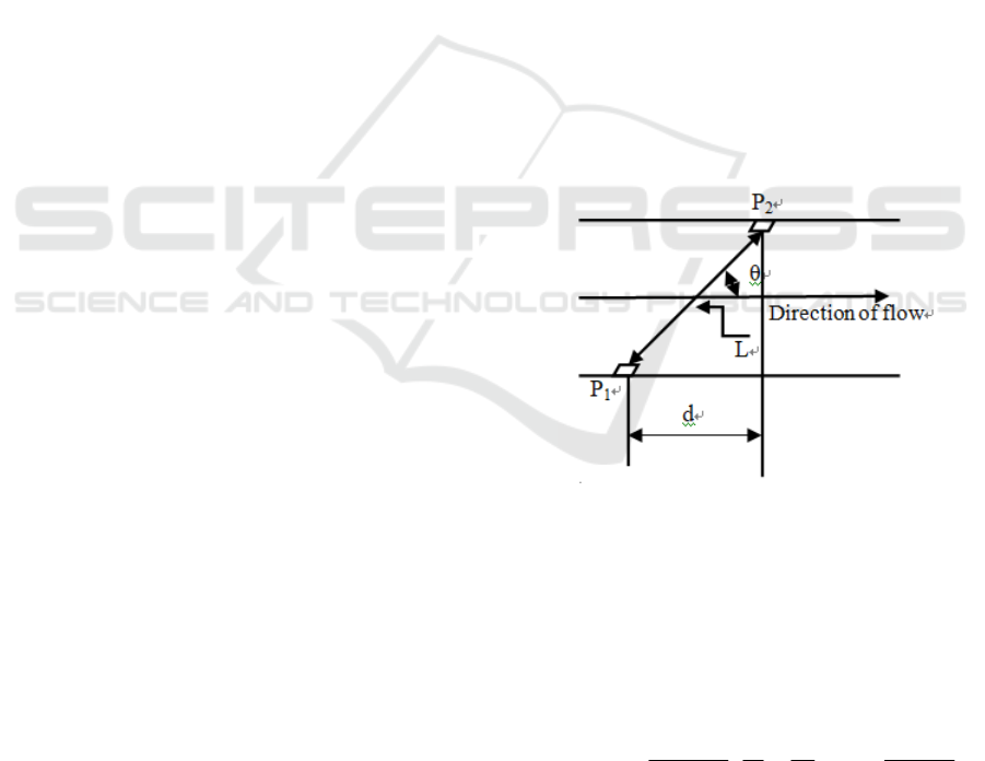
Fig. 1 principle diagram of time difference method.
P1, P2 are two ultrasonic transducers, v is the
flow velocity of fluid, and θ is the angle between
P1P2 and the fluid flow direction; d is the linear
distance between P1 and P2, L is the vertical length
between P1 and P2, c is the sonic velocity. First, P1
is the transmitter and P2 as the receiver, propagation
time is downstream time t1:
2
21
)
2
sin
()
11
(
cos2
L
tt
L
SQ
In the formula above, the influence of the
temperature change to the measuring result is
avoided, and the accuracy of the flow measurement
is ensured.
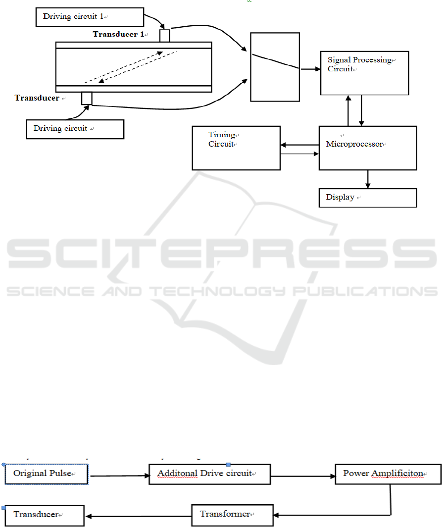
3 THE OVERALL DESIGN OF
ULTRASONIC GAS FLOW
METER
The overall structure of ultrasonic gas flow meter is
shown in Figure 2, including ultrasonic transducer
drive circuit, analog switch, signal processing circuit,
single-chip microcomputer, timing circuit, display
circuit.[6]
Fig. 2 the overall block diagram of ultrasonic gas flow meter.
4 THE CHOICE OF THE
ULTRASONIC TRANSDUCER
AND DESIGN OF THE
DRIVING CIRCUIT
4.1 Selection of Ultrasonic Transducer
Because of measuring gas flow, the center frequency
of the transducer can only be in the range of tens
KHz to hundreds KHz. In order to transducer are: (1)
the center frequency: 120 kHz; get large output
signal, the area of transducer chip must be as large
as possible, with large driving power, strong
ultrasonic signal is output, which will alleviate the
burden of the sequential circuit and improve the
stability and accuracy of the overall system signal.
In this design, the diameter of the transducer
wafer is about 15mm. The performance parameters
of the selected ultrasonic.
(2) the driving pulse amplitude: 300V; (3) band
width: 2 KHz; (4) the static capacitance: 500p (2600
ohm impedance equivalent in 120 kHz).
4.2 Ultrasonic Transducer Drive Circuit
Design
It is not easy to produce amplitude 300V pulse
directly. In this design, the basic ideas is to produce
small amplitude square wave with same frequency
first, then a transformer is used to realise 300V pulse
after amplitude amplification and power
amplification. The diagram of driving circuit is
shown in Figure 3.
Fig. 3 Integral block diagram of driving circuit .
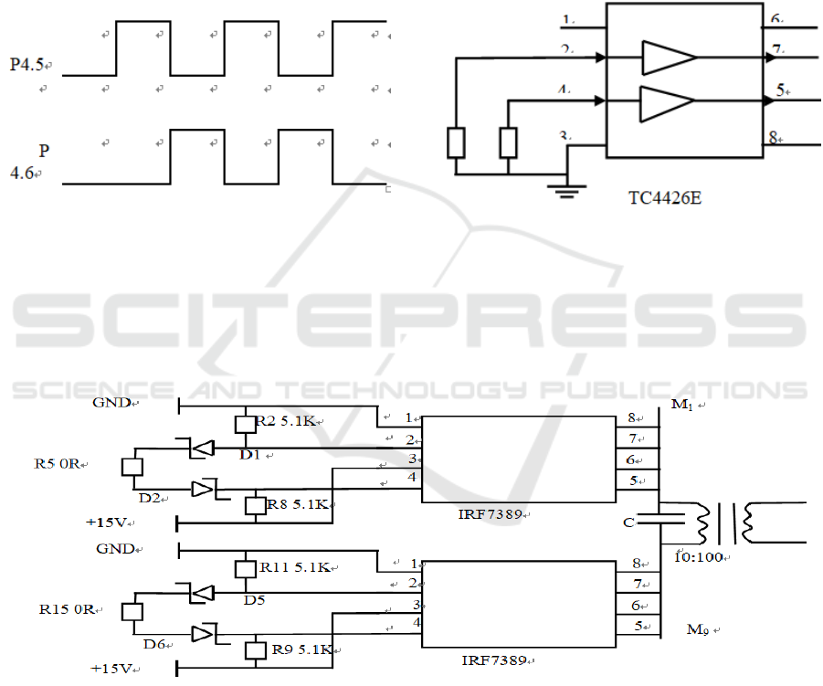
4.3 Primary Pulse Generation Circuit
Design
The initial source of the driving pulse is the pin of
the single chip microcomputer Msp430f149 which
outputs the +3.3V square wave pulse with 120 KHz
frequency. Each transducer of the driving pulse is
divided into two parts, for a transducer using the
microcontroller pin P4.3 and P4.4, and the other one
using pin P4.5 and P4.6. The drive pulse is shown in
figure 4:
Fig. 4 Initial driving pulse
4.4 Power Amplifier Circuit Design
The voltage of transformer primary coil is +30V
while the transform ation ratio is 10:100. MCU
sends out +3.3V pulse amplitude needing amplitude
amplification and power amplification before
reaching +30V. IRF7389 power field effect tube is
used to realise power amplifier, whose parameters
are VDSS = + 30V, on the resistance RDS (ON) =
0.029 ohm (N channel) and 0.058 ohm (P channel),
ID = 4A. Due to its large junction capacitance
(1000PF), IRF7389 needs 15mA to work. A single
pin of Msp430F149 can only output the maximum
current 3mA, unable to meet the requirements.
Therefore additional driver chips must be used. In
this paper, the TC4426EOA field effect transistor
driver is selected, and the driving circuit schematic
diagram is shown in Figure 5.
Fig. 5 Schematic diagram of IRF7389.
As shown in Figure 5, driving circuit based on
TC4426EOA converts the +3.3 V signal to +15V
pulse with 100mA current output. It can drive the
IRF7389 power circuit, the power application circuit
with the transformer is shown in Figure 6.
Fig. 6 Power amplifier and transformer circuit diagram.
Two pieces of IRF7389 is used in the circuit.
Each chip comprises two power field effect tube, a
p-channel and an n-channel tube. When it outputs
high level signal, n-channel tube works. When the
low level signal is outputs, p-channel tube works.
Therefore, it can guarantee the value of the voltage
between the M1 and M9 is 30V; 300V amplitude
can be gotten after 10:100 transformer. At same time,
the current can meet the requirements to drive
ultrasonic transducer. The output signal of the
ultrasonic transducer is shown in Figure 7. The
amplitude of the signal has reached the peak-peak
value of 1V, which provides convenience for the
design of the subsequent processing circuit.
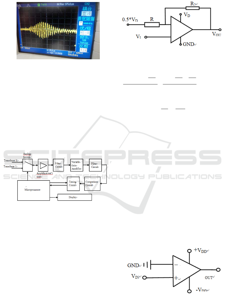
Fig. 7 Ultrasonic signals received by the receiving
transducer.
5 SIGNAL PROCESSING CIRCUIT
DESIGN
Signal processing circuit is the ultrasonic signal
receiving and processing circuit, including:
switching circuit, no-inverting amplifier circuit,
filter circuit, variable gain amplifier and comparison
circuit, timing circuit, LCD display circuit, and
several other parts. The overall structure of the
receiving circuit is shown in Figure 8.
Fig. 8 Overall block diagram of signal receiving circuit.
5.1 Signal Amplification Circuit Design
Midpoint voltage single supply noninverting
amplifying circuit is used in the design who can
realize the signal extraction and amplification
because of its large input impedance and can avoid
the use of negative power supply to reduce the noise
of the system and save the use of components.
Operational amplifier in this design is MAX4331,
circuit as shown in Figure 9.
The relationship between the input signal and the
output signal of the circuit can be calculated by the
following formula:
Figure 9 Midpoint voltage no inverting amplifier circuit
diagram.
Through the above formula, we can know that
the output signal is superimposed on the half power
supply, so in single power circuit positive and
negative signal can be amplified at the same time,
the magnification times are 2. Amplification factor
is small because non inverting amplifier input
impedance is too large to lead to large noise that will
cause difficulty to design the later filter circuit.
6 COMPARISON CIRCUIT DESIGN
In order to accurately measure the time interval, it is
necessary to have a zero crossing comparison circuit,
after which the ultrosnic signal is converted into
square wave to trigger time chip to record the time
of transmission. The comparator in the comparison
circuit is MAXIM Company’s MAX998, the
circuit as shown in fig.
Fig. 10 Schematic diagram of zero crossing.
2
)
2
()
2
(
12
R
VV
V
R
V
VV
DDDD
IN
DD
INOUT
2
)1(
1
2 DD
INOUT
V
R
R
VV
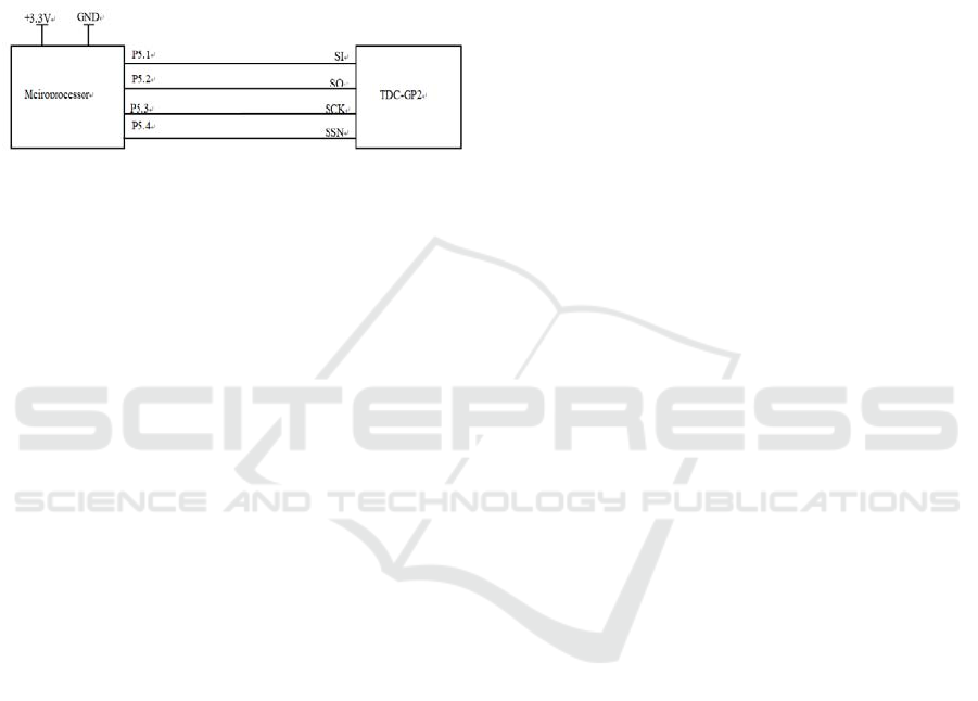
7 TIMING MODULE CIRCUIT
DESIGN
Time chip TG-2 is used in this design to measure
time difference. TG-2 has two kinds of modes. In
this design, mode 2 is choiced: 50ps time resolution,
500ns - 4ms measurement range, rising edge or
falling edge trigger. The interface circuit between
microcomputer MSP430f149 and time chip TG-2
circuit is shown in figure .
Figure 11 TDC-GP2 and MSP430 MCU SPI interface
circuit.
REFRENCES
1. EDGAR. Natural Gas Flow Measurement in the 21st
Century. Pipeline&Gas Journal [J]. 1999,26(7):18-
21.
2. Jesse Yoder.Ultrasonic Meters:A Natural Choice
to Measure Gas Flow.Pipeline&Gas
3. Journal, 2000(781):224-7550.
4. LYNNWORTH L C, LIU Yi.Ultrasonic Flowmeters:
Half-Century Progress Report,1995 2005[J].Science
Dreict,2006(44):1371-1378.
5. Furio Cascetta, Giuseppe Rotondo. Effects of
intermittent flows on turbine gas meters accuracy.
Measurement [J]. 2015, 69(5): 280 – 286
6. Denghui He, Bofeng Bai. A new correlation for wet
gas flow rate measurement with Venturi meter based
on two-phase mass flow coefficient. Measurement [J].
2014, 58(3): 61 – 67
7. [6] M. Farzaneh-Gord, S. Parvizi, A. Arabkoohsar, L.
Machado, R.N.N. Koury. Potential use of capillary
tube thermal mass flow meters to measure residential
natural gas consumption. Journal of Natural Gas
Science and Engineering [J]. 2015, 22(6): 540-550
