
Lead Sulphide Colloidal Quantum Dots for Sensing Applications
A. De Iacovo, C. Venettacci, S. A. Bruno and L. Colace
Department of Enginnering, University Roma Tre, Via Vito Volterra 62, Rome, Italy
Keywords: Pbs Colloidal Quantum Dots, Fire Detector, Gas Detector.
Abstract: Colloidal Quantum Dots (CQD) have been widely studied for their peculiar optical characteristics such as
enhanced optical absorption and tunable absorption spectrum. Many different photodetectors have been
proposed but overall performance is still poor from the point of view of the bandwidth and noise performance.
Here we propose the employment of a PbS QD photoconductor as an ultra-high sensitivity fire detector,
exploiting the outstanding device responsivity at low optical powers. Moreover, we demonstrate the
outstanding flexibility of CQD based devices, employing our detectors also as simple pollution gas sensors
for NO
2
detection.
1 INTRODUCTION
Colloidal Quantum Dots (CQD) are semiconductor
nanoparticles directly synthesized and dispersed in
solution. The synthesis process is straightforward and
does not require high vacuum or high temperature (Pu
et al. 2018). Moreover, the final material
characteristics can be easily tailored through the
modification of simple parameters such as reaction
time and temperature. Being nano-sized, the quantum
dots show peculiar optical, electronic and chemical
characteristics such as enhanced optical absorption
and resonant absorption spectra (Moreels et al. 2009),
ease of doping (even after material synthesis and
directly on the deposition substrate) (Kagan et al.
2016) and outstanding reactivity with several
chemical species thanks to the high surface-to-
volume ratio. Being dependent on the nanoparticle
size, all these characteristics can be easily tailored
during the QD synthesis, leading to a variety of
similar colloidal materials with a vast range of
physical properties.
Thanks to their characteristics, colloidal quantum
dots have been employed for the realization of several
different kind of devices, such as photodetectors (De
Iacovo et al. 2016), solar cells (Sargent 2012), light
emitting diodes (Caruge et al. 2008) and
chemoresistors (Liu et al. 2014). In general, all these
devices exploit the ease of formation of QD films and
either their outstanding optical properties or their very
high surface-to-volume ratio and chemical reactivity.
Among several different materials in the class of
CQDs, lead sulphide (PbS) has been widely
employed for the fabrication of near-infrared
photodetectors; it’s absorption edge can easily be
tuned, by quantum-confinement effect, from 900nm
to 1.8μm (Moreels et al. 2009) and its synthesis route
is well established, producing colloids that are stable
over a long period of time. The as-synthesized colloid
is usually stabilized with an organic, long-chained
capping agent such as oleic acid. Such colloids can be
readily deposited on a variety of substrates to produce
QD films; in this case, however, the nanoparticles in
the solid film are arranged with a mean distance twice
as long as the molecular chain of the capping agent.
Such a distance is, typically, too long for the film to
be conductive because charges cannot easily tunnel
from one dot to another. To enhance the film
conductivity, a ligand exchange procedure is usually
necessary. The long-chained ligands are stripped
away from the QD surface (either in solution or
directly from the deposited film) and substituted with
shorter ones, thus enabling charge transfer between
neighbouring nanocrystals.
This approach can be carried out on a variety of
substrates, comprising silicon and SiO
2
. PbS QDs
have been employed for the realization of
photodetectors and transistors directly on silicon
substrates, thus enabling their integration with silicon
electronics in a more-than-Moore framework (Balazs
et al. 2014). Nevertheless, the resulting devices still
show poor performance in terms of noise and
bandwidth and the technology is not yet comparable
De Iacovo, A., Venettacci, C., Bruno, S. and Colace, L.
Lead Sulphide Colloidal Quantum Dots for Sensing Applications.
DOI: 10.5220/0007444002350240
In Proceedings of the 7th International Conference on Photonics, Optics and Laser Technology (PHOTOPTICS 2019), pages 235-240
ISBN: 978-989-758-364-3
Copyright
c
2019 by SCITEPRESS – Science and Technology Publications, Lda. All rights reserved
235

to other well-established more-than-Moore
approaches such as Ge-on-Si (Sorianello et al. 2010)
(Sorianello et al., 2015). Poor device performance can
usually be attributed to very low electron mobility
and high noise which, in turn, limit the device
bandwidth and detectivity (De Iacovo at al. 2017).
For these reasons, CQD based devices are more
suitable for sensing applications, where high
sensitivity and low bandwidth are required.
In this paper we show our recent work with PbS
QD devices for sensing applications both in the
optoelectronic and gas sensing field. In particular, we
propose a high-gain, visible-blind, photoconducting
photodetector for indoor flame detection and a
chemoresistive gas sensor for NO2.
2 DEVICE FABRICATION
The devices have been fabricated employing a
commercial 10mg/mL PbS QD solution in toluene
with mean particle diameter of 5nm (Sigma-Aldrich).
This particular type of nanoparticle has a first
excitonic absorption peak located near 1360nm. The
nanoparticles are capped with oleic acid and the first
fabrication step consists in the removal of the long-
chained ligand by centrifugation in excess methanol.
The precipitated nanocrystals are then washed with
methanol and any residual solvent is evaporated in a
vacuum desiccator. The QDs are redispersed in
octane with a 0.8mg/mL final concentration. The new
QD solution is drop casted on a SiO
2
substrate with
pre-patterned gold interdigitated contacts and the
devices are kept in a desiccator until full solvent
evaporation. Butylamine is then drop-casted onto the
QD film. In this step the amine ligates to the
nanocrystal surface and the QDs in the film are
rearranged with a short mean distance (0.6nm)
corresponding to the length of the organic molecule.
QD and butylamine drop-casting are repeated 10
times to create a nanocrystal film with e mean
thickness of 1μm. Eventually, the devices are rinsed
with methanol for 2 hours to remove all the
butylamine and improve QD packing (Konstantatos
et al., 2006). For the fabrication of the visible-blind
photodetectors, the devices are enclosed in a
packaging with a silicon optical window that acts as
a filter for visible wavelengths. Conversely, devices
meant as gas sensors are readily usable after
fabrication.
3 VISIBLE-BLIND
PHOTODETECTORS AND
FLAME SENSORS
The photodetectors where initially characterized in
terms of current-voltage characteristics to verify the
device resistivity and the ohmicity of the Au-QD
contact. Fig. 1 shows the resistance of three different
devices with interdigitated finger spacings ranging
from 5 to 20μm. As expected, the resistance increases
with the finger spacing. The devices show a linear I-
V characteristic (Fig. 1, inset) confirming the
ohmicity of the Au-QD contact.
Figure 1: Device resistivity vs. interdigitated finger
spacing. Inset: voltage-current characteristics of a 5μm
device.
A semiconductor laser at 1300nm has been employed
for the characterization of the device’s
photoresponse. Fig. 2 shows the measured
responsivity and its dependence on the applied bias.
As expected for a photoconductor, responsivity is
proportional to the applied bias and at 1V it is higher
than 1A/W. Thus, the photodetector shows a
photoconductive gain. This phenomenon has been
previously observed in similar devices and should be
attributed to the long electron lifetime due to the
presence of deep electron traps with a reduced cross-
section for holes (Konstantatos et al. 2007). The
presence of such a trapping mechanism usually
induces a nonlinear response in the photodetector. At
low incident optical power, in fact, all the
photogenerated electrons can be trapped and the
photoconductive gain is maximum; conversely, when
the photogenerated carriers outnumber the available
10
5
10
6
10
7
10
8
5 10 15 20 25 30 35
Resistance [
Finger spacing [m]
-1.5 10
-6
-1 10
-6
-5 10
-7
0
5 10
-7
1 10
-6
1.5 10
-6
-1.5 -1 -0.5 0 0.5 1 1.5
Current [A]
Applied bias [V]
PHOTOPTICS 2019 - 7th International Conference on Photonics, Optics and Laser Technology
236
trap states, some electron can be swept throughout the
device and can be collected at the gold contacts in a
time much shorter than the mean electron lifetime. In
this case the overall photoconductive gain is reduced.
In order to verify this behavior, we characterized the
device varying the incident optical power. Fig. 3
shows the obtained R vs. P characteristics. As
Figure 2: Responsivity vs. voltage characteristics of a 5μm
photodetector.
expected, the responsivity has a strong dependence on
the optical power and reaches a plateau around 5nW.
It should be observed that, given the low operating
voltage, our devices show a responsivity performance
comparable with state-of-the-art PbS QD
photoconductors (Saran et al. 2016).
The high responsivity at low incident optical
power can be exploited for the realization of detectors
for fire and flame sensing applications. It is well
known that a hot body emits an optical radiation
whose spectrum is described by Planck’s law as
defined in (1), where B is the spectral irradiance at the
optical frequency υ and temperature T, h is the Planck
constant, K is the Boltzmann constant and c is the
speed of light.
(1)
A flame, burning between 900 and 1100°C
(Babrauskas 1980), emits a radiation with a wide
spectrum from the visible wavelengths to the infrared,
peaked at around 1800nm. Being highly sensitive in
the NIR region of the spectrum, the PbS CQD
photoconductor can be easily employed for flame
detection but, in order to avoid false detection due to
ambient illumination, a visible light filter must be
included. As previously mentioned, we encapsulated
the photodetector in a packaging provided with a
silicon window which completely absorbs radiation
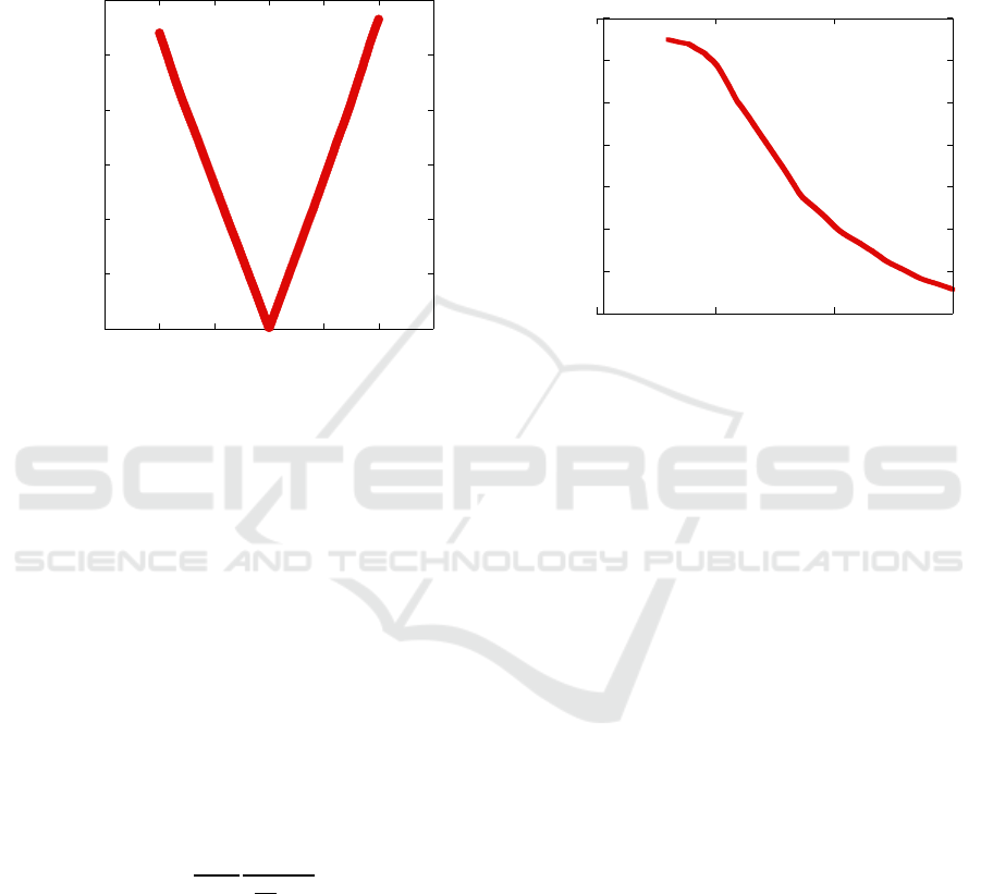
in the visible range. Fig. 4 shows both the spectral
responses of the unpackaged (red curve) and
packaged (blue curve) photodetector. The silicon
filter absorbs all the light below 900nm. Fig. 4 also
shows the presence of the excitonic absorption peak
of the PbS QDs at 1360nm.
Figure 3: Responsivity vs. incident optical power.
The removal of any radiation with λ<900nm implies
that the device can be effectively employed for flame
detection in an indoor environment. Light sources used
in domestic environment, in fact, don’t emit any
infrared radiation that could interfere with the flame
detection. Conversely, sunlight could prevent the
detector’s operation. We tested our device in a closed
room with standard office illumination (neon lamps,
250 lm/m2) lighting a wax candle in front of the
photodetector and varying the distance between the
candle and the detector surface. Fig. 5 shows the
percent variation of the measured current with respect
to the dark current at 1V bias; as expected,
photocurrent follows an inverse square law with the
flame distance.
We also measured the mean dark current and its
standard deviation over 10 minutes, obtaining σ =
0.25%. We defined a flame detection threshold that is
20 times larger than σ (5%). This threshold and its
intercept with the detection curve are represented
with dashed lines in Fig. 5. The detection threshold is
reached when the candle is lit 17.9m from the
detector’s surface.
0
0.5
1
1.5
2
2.5
3
-1.5 -1 -0.5 0 0.5 1 1.5
Responsivity [A/W]
Applied bias [V]
P
opt
= 1W @ 1300nm
0
5
10
15
20
25
30
35
1 10 100 1000
Responsivity [A/W]
Optical power [nW]
Applied bias = 1V
= 1300nm
Lead Sulphide Colloidal Quantum Dots for Sensing Applications
237
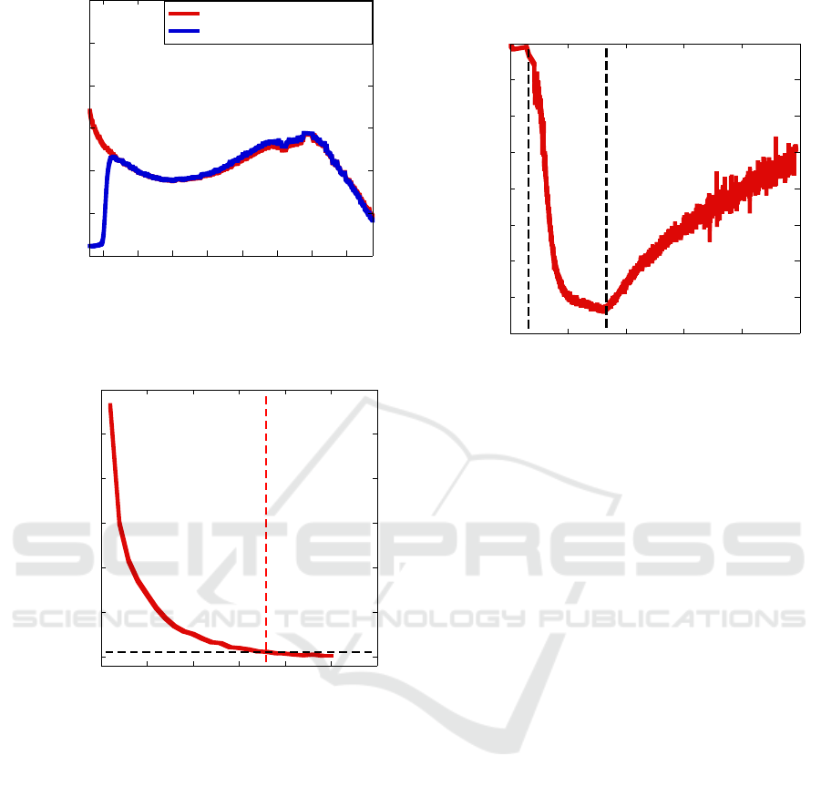
Figure 4: Spectral response of the PbS CQD photodetector
with (blue curve) and without (red curve) the silicon filter.
Figure 5: Detector current variation vs. candle flame
distance.
Given the device resistance and the applied
voltage, we also evaluated the mean power
dissipation of the flame detector as P
diss
= V
2
/R≈
1.2μW.
Eventually, we verified that the detector response
was not modified with respect to environment
illumination. We tested our device from complete
dark to strong indoor illumination (neon and LED
lamps, 1000-2000 lm/m
2
) and could not observe any
difference in the detector behavior.
Our results demonstrate that a PbS QD
photodetector can be effectively employed as a high-
sensitivity flame detector for indoor safety systems,
providing very high detection distance and low power
consumption.
4 POLLUTION GAS SENSOR
Figure 6: PbS QD sensor resistance variation in response to
50ppmmol NO
2
.
QD surface chemistry plays a key role in the
determination of the electronic characteristics of
CQD electron devices (Brown et al., 2014); oxidation
of the QD film, in particular, has shown dramatic
effects on the performance of PbS photodetectors (De
Iacovo et al., 2016). One of the main class of polluting
gases is represented by nitrous oxides (NO
x
) and we
tested our devices as gas sensors for NO
2
detection.
The devices were wire bonded to a custom chip
carrier and inserted into an enclosed test chamber
where we fluxed pure nitrogen and NO
2
, varying the
proportional flux of the pollutant gas. Fig. 6 shows
the typical resistance variation of a PbS QD resistor
(finger spacing = 20μm) in response to 50ppmmol of
NO
2
. The sensor shows a slow response to the gas,
reaching a resistance plateau after 10 minutes of
fluxing. Also, gas desorption is very slow and
complete recovery happens only after 1.5 hours.
We evaluated the sensor response to different gas
concentrations. Fig. 7 shows the percent resistance
variation with respect to the ppm of NO
2
fluxed into
the measurement chamber and the corresponding
linear fit. We evaluated a resistance variation of
1.5%/ppm corresponding to 3MΩ/pmm.
Our results are promising for future development
of PbS CQD based sensors for pollutant gas detection,
nevertheless, the slow response are recovery time are
still an issue. A possible approach to enhance device
response and recovery time should consist in a
reduction of the thickness of the QD film.
0
2000
4000
6000
8000
1 10
4
1.2 10
4
880 960 1040 1120 1200 1280 1360 1440
Absorption (w/o Si filter)
Absorption (w/ Si filter)
Photoresponse [a.u.]
Wavelength [nm]
0
50
100
150
200
250
300
0 5 10 15 20 25 30
I
flame
/I
dark
[%]
Flame distance [m]
20
30
40
50
60
70
80
90
100
0 1000 2000 3000 4000 5000
R [%]
Time [s]
Gas in
Gas out
50ppmmol NO
2
PHOTOPTICS 2019 - 7th International Conference on Photonics, Optics and Laser Technology
238

Figure 7: Device resistance variation for different NO
2
concentrations. Experimental data (points) and linear fit
(line).
We determined the sensor noise by continuously
measuring its resistance with no gas flow for 10
minutes and determining the standard deviation of the
acquired data. We employed this data to extrapolate
the theoretical detection limit of our sensor obtaining
a minimum detectable NO2 concentration of 4.9ppb.
Even if our detector shows lower performance if
compared to other PbS QD based NO
2
sensors (Song
et al., 2018), it should be noted that we propose a
device that is already integrated on a Si/SiO
2
substrate
and that, consequently, could be easily coupled with
readout electronics to produce a standalone NO2 gas
sensor with a more-than-Moore approach. Moreover,
device parameters such as QD film thickness and
metal finger spacing could be optimized to enhance
the device response. This analysis is, however, out of
the scope of this paper and will be discussed in future
publications.
5 CONCLUSIONS
In this paper we showed our results with optical and
chemical sensors based on PbS colloidal quantum
dots. We showed how the same CQD device, with
only slight modifications in the fabrication process,
can have manifold applications for different sensing
purposes. We proposed a novel fire detector with
ultra-high sensitivity for indoor applications and a
pollution gas sensor integrated on a Si/SiO
2
substrate,
defining a strategy for future sensor integration with
silicon electronics.
REFERENCES
Babrauskas, V., 1980. Estimating room flashover
potential. Fire Technology, 16(2), 94-103.
Balazs, D. M., Nugraha, M. I., Bisri, S. Z., Sytnyk, M.,
Heiss, W., and Loi, M. A., 2014. Reducing charge
trapping in PbS colloidal quantum dot solids. Applied
Physics Letters, 104(11), 112104.
Brown, P. R., Kim, D., Lunt, R. R., Zhao, N., Bawendi, M.
G., Grossman, J. C., and Bulovi, V., 2014. Energy
level modification in lead sulfide quantum dot thin
films through ligand exchange. ACS nano, 8(6), 5863-
5872.
Caruge, J. M., Halpert, J. E., Wood, V., Bulovi, V., and
Bawendi, M. G., 2008. Colloidal quantum-dot light-
emitting diodes with metal-oxide charge transport
layers. Nature photonics, 2(4), 247.
De Iacovo, A., Colace, L., Scopa, L., and Foglia, S., 2016.
Near-infrared photodetectors based on PbS colloidal
quantum dots. In Optical Sensing and Detection
IV (Vol. 9899, p. 989908). International Society for
Optics and Photonics.
De Iacovo, A., Venettacci, C., Colace, L., Scopa, L., and
Foglia, S., 2016. PbS Colloidal Quantum Dot
Photodetectors operating in the near infrared. Scientific
reports, 6, 37913.
De Iacovo, A., Venettacci, C., Colace, L., Scopa, L., and
Foglia, S., 2017. Noise performance of PbS colloidal
quantum dot photodetectors. Applied Physics
Letters, 111(21), 211104.
Kagan, C. R., Lifshitz, E., Sargent, E. H., and Talapin, D.
V. (2016). Building devices from colloidal quantum
dots. Science, 353(6302), aac5523.
Konstantatos, G., Howard, I., Fischer, A., Hoogland, S.,
Clifford, J., Klem, E., Levina, L., and Sargent, E. H.,
2006. Ultrasensitive solution-cast quantum dot
photodetectors. Nature, 442(7099), 180.
Konstantatos, G., and Sargent, E. H., 2007. PbS colloidal
quantum dot photoconductive photodetectors:
Transport, traps, and gain. Applied Physics
Letters, 91(17), 173505.
Liu, H., Li, M., Voznyy, O., Hu, L., Fu, Q., Zhou, D., Xia,
Z., Sargent, E. H., and Tang, J., 2014. Physically
flexible, rapid‐response gas sensor based on colloidal
quantum dot solids. Advanced Materials, 26(17), 2718-
2724.
Moreels, I., Lambert, K., Smeets, D., De Muynck, D.,
Nollet, T., Martins, J. C., Vanhaecke, F., Vantomme,
A., Delerue, C., Allan, G., and Hens, Z., 2009. Size-
dependent optical properties of colloidal PbS quantum
dots. ACS nano, 3(10), 3023-3030.
Pu, Y., Cai, F., Wang, D., Wang, J. X., and Chen, J. F.,
2018. Colloidal synthesis of semiconductor quantum
dots toward large-scale production: A
review. Industrial and Engineering Chemistry
Research, 57(6), 1790-1802.
Saran, R., and Curry, R. J., 2016. Lead sulphide nanocrystal
photodetector technologies. Nature Photonics, 10(2),
81.
20
30
40
50
60
70
80
90
0 10 20 30 40 50 60
R [%]
NO
2
concentration [ppmmol]
Lead Sulphide Colloidal Quantum Dots for Sensing Applications
239

Sargent, E. H., 2012. Colloidal quantum dot solar
cells. Nature photonics, 6(3), 133.
Song, Z., Huang, Z., Liu, J., Hu, Z., Zhang, J., Zhang, G.,
Yi, F., Jiang, S., Lian, J., Yan, J., Zang, J., and Liu, H.,
2018. Fully Stretchable and Humidity-Resistant
Quantum Dot Gas Sensors. ACS sensors.
Sorianello, V., De Iacovo, A., Colace, L., Assanto, G.,
Fulgoni, D., Nash, L., and Palmer, M. (2010).
Germanium on insulator near-infrared photodetectors
fabricated by layer transfer. Thin Solid Films, 518(9),
2501-2504.
Sorianello, V., De Angelis, G., De Iacovo, A., Colace, L.,
Faralli, S., and Romagnoli, M. (2015). High
responsivity SiGe heterojunction phototransistor on
silicon photonics platform. Optics express, 23(22),
28163-28169.
PHOTOPTICS 2019 - 7th International Conference on Photonics, Optics and Laser Technology
240
