
Introducing Advanced Freeform Optic Design to Li-Fi Technology
René Kirrbach
1,2
, Benjamin Jakob
1,2
and Alexander Noack
1
1
Fraunhofer IPMS, Maria-Reiche-Straße 2, Dresden, Germany
2
Department of Electrical and Computer Engineering, TU Dresden, Dresden, Germany
Keywords: Composite Ray Mapping, Freeform Optics, Fresnel Lenses, Li-Fi, Optical Wireless Communications, TIR
Optic.
Abstract: The paper considers the potential of freeform optics for Li-Fi technology and presents design approaches for
transmitter and receiver optics using ray mapping methodology and freeform Fresnel lens, respectively.
Simulation results are then presented for models validation.
1 INTRODUCTION
The proceeding digitalization of our environment leads
to continuously increasing mobile data traffic. The
capacity provided by current radio frequency (RF)
based wireless technologies such as Wi-Fi, Bluetooth
will not be sufficient in the future, due to their limited
frequency bands. Inter-channel interference is an
emerging issue that degenerates data rate and latency
of wireless links in crowded areas. The so-called
“spectrum crunch” can be faced by introducing new
technologies with different carrier frequencies. Besides
intensive research in the field of millimeter-wave
based communications (Rappaport et al., 2013), Li-Fi
technology becomes more and more popular. Li-Fi
utilizes visible or invisible optical wireless
communication links that offer high-speed and low
latency data transfer trough spatially well-defined
communication channels. This allows to design
cellular networks and to reduce inter-channel
interference.
In the past decade different aspects of the Li-Fi
technology emerged rapidly. Various modulation
schemes were investigated (Islim et al., 2016), new
emitters were developed (Ferreira et al., 2016) and
integration of Li-Fi into existing networks was studied
(Wu et al., 2017). However, despite investigation
concerning fluorescence concentrators (Collins et al.,
2014), modern optic design methodology for Li-Fi was
not in focus of the scientific discourse. Typically,
simple lenses are used for beam shaping and optical
amplification. But these cannot fully serve current
trends like an ongoing miniaturization of Li-Fi
transceivers in order to allow their integration into
other devices. Scaling down the optics is directly
connected to performance degeneration. This is due to
the extended source problem at transmitter side and
reduced receiver gain. Advanced freeform optics can
compensate the performance degeneration and provide
compact, high-performance solutions precisely
tailored to the application. For example, providing Li-
Fi connectivity within a corridor can effectively be
realized by shaping rectangular spots.
This paper demonstrates the potential of freeform
optics for Li-Fi technology and gives an overview over
suitable optical design methods. The rest of the paper
is organized as follows: in chapter two fundamental
requirements for Li-Fi optic modules are defined and
limitations of standard lenses are shown. Chapter three
provides an overview over different optical design
concepts. In chapter four we present design examples
of freeform transmitter and receiver optics and
characterize them with optical simulations. Finally,
chapter five gives a short summary.
2 FUNDAMENTALS
As Figure 1 illustrates, a Li-Fi module consists of a
transmitter (Tx) and a receiver (Rx). The transmitter
uses light emitting diodes (LEDs) or laser diodes (LDs)
for signal transmission, whereas the receiver
incorporates a photodiode (PD) for signal detection.
Both parts are characterized by their field-of-view
(FOV). Typically, both FOVs are designed equally.
However, in certain application scenarios they may
differ. If Li-Fi connectivity is provided within a
corridor, the fixed transmitter at the ceiling shapes a
248
Kirrbach, R., Jakob, B. and Noack, A.
Introducing Advanced Freeform Optic Design to Li-Fi Technology.
DOI: 10.5220/0007471802480254
In Proceedings of the 7th International Conference on Photonics, Optics and Laser Technology (PHOTOPTICS 2019), pages 248-254
ISBN: 978-989-758-364-3
Copyright
c
2019 by SCITEPRESS – Science and Technology Publications, Lda. All rights reserved

rectangular spot. The receiver of the mobile device
below has a rotationally symmetric FOV due to the
unknown orientation of both devices to each other.
Figure 1: Li-Fi transceiver consisting of a transmitter (a)
and a receiver (b). Simple systems incorporate spherical
lenses as shown here.
The optical link is further characterized by its
dynamic range which defines the spatial distance
where data transmission is possible. It is limited by a
minimum and a maximum range. Below the minimum
distance the signal is too strong and the receiver runs
into saturation. Above the maximum distance the
signal level is below the sensitivity of the receiver. The
receiver amplifier can use automatic gain control to
improve the dynamic range. However, this approach
has its limits. For a maximization of the dynamic range
the transmitter and receiver must exhibit a
homogenous behavior over their FOV. This can easily
be understood if we assume for instance a strong peak
in the transmitter’s emission profile. The peak raises
the minimum communication distance and
consequently lowers the dynamic range.
2.1 Transmitter Optics Requirements
As already mentioned, LEDs or LDs are used as
emitters. LDs exhibit small emission angles.
Sometimes even standard aspheric lenses allow
sufficient beam shaping. LEDs are isotropic emitters.
Thus, efficient optic design for LEDs is more
sophisticated. Fortunately, Li-Fi technology can profit
from advances in freeform illumination design where
LEDs are omnipresent nowadays. In contrast to
illumination design, efficiency and homogeneity is
even more crucial since it refers directly to range, data
rate and bit error rate. Moreover, the transmitter’s
optical output power might be limited due to
bandwidth requirements or because of the limited
power budget of mobile devices.
The communication spot can be defined as the area,
where the irradiance E is larger than the minimum
irradiance E
min
required for communication. The
transmitter’s efficiency
is the power that reaches
the FOV divided by the total emitted power. However,
does not pay attention to the power distribution
within the FOV. If the transceiver has a bit-loading
mechanism, it adjusts its data rate to receiver’s current
signal level.
Yet, low-latency transceivers typically have simple
modulation schemes with fixed data rate. They require
a defined minimum receiver signal level and thus a
minimum irradiance E
min
in order to fulfil the
specification, i.e. ensuring a bit error rate. An
irradiance peak within the FOV gives no benefit, since
the specification is already fulfilled with E
min
. In fact
such a peak actually reduces the dynamic range by
increasing the minimum communication distance as
mentioned before. Therefore, it is better to equally
distribute the power within the FOV to raise E
min
in
order to maximize the range of the link. Hence, for
transceivers with fixed data rate we define a more
powerful figure of merit by combining efficiency and
uniformity: equation (1) defines the effective
transmitter efficiency
as the ratio of the
minimum irradiance E
min
within the FOV at the
maximum distance produced by the optic to
.
This
is the irradiance achieved by an ideal
optic, which concentrates 100 % of the emitted power
P
Tx
homogenously into the FOV and forms a so-called
tophat profile. It is calculated by dividing the emitted
power P
Tx
by the illuminated area A
t
.
(1)
Figure 2 illustrates a numerical example, where the
FOV should have a half-angle of 17°. The LED
SFH4451 (Osram Opto Semiconductors, 2016) has an
angle of half intensity of 17° and thus seems to be well
suited. However, only about 30.7 % of the emitted
power P
Tx
is within the FOV and the effective
transmitter efficiency is only
. In
contrast, an ideal optic with
reaches an
minimum irradiance E
min
which is 5.94 times (7.7 dB)
higher. This corresponds to an increase of the
communication range by a factor of 2.4 if the data rate
is fixed. Simple transmitters use spherical lenses in
order to improve the performance, as shown in
Figure 1a. Table 1 summarizes the measures of all
three emission profiles. Using the lens LA1805.1
(Thorlabs, 2018) nearly doubles the efficiency to
. It can be seen, that the irradiance profile
is still very inhomogeneous, leading to bad dynamic
range and an effective efficiency of only
. Aspheric lenses could improve the
performance, but there are still two problems: First, not
all of the emitted power reaches the lens. Second, if
standard lenses are used the design freedom is low and
it is hard or even impossible to find an aspheric lens
that ideally fits.
LED / LD
PD
d
d
(a)
(b)
Introducing Advanced Freeform Optic Design to Li-Fi Technology
249

Figure 2: Irradiance along x-axis in 1 m distance for Osram
SFH4451 LED without an additional lens and with the
spherical lens LA1805.1. The distance d between lens and
PD is 9.6 mm (Figure 1a) and the optical power P
Tx
is
55 mW. The tophat represents the ideal irradiance profile.
Table 1: Measures of the emission profiles from Figure 2.
Transmitter
SFH 4451,
no optics
0.307
0.314×10
-5
W/cm²
0.168
SFH 4451 +
LA1805.1
0.595
0.529×10
-5
W/cm²
0.282
Ideal tophat
1
1.873×10
-5
W/cm²
1
2.2 Receiver Optics Requirements
The receiver optic introduces an optical gain g by
concentrating the incident signal onto the PD.
It is well known that the optical gain g of classical
optics is Étendue limited. In a 3D system g can be
calculated by using equation (2) (Welford et al., 1989),
where n
1
denotes the optic’s refractive index and n
2
the
refractive index of the surrounding medium, which is
typically air. The optic’s half acceptance angle is
.
describes the incident angle of the boundary rays
from the optic to the PD chip. The maximum
theoretical optical gain g
max
is reached for
(Welford et al., 1989). Therefore, the optic has to be in
direct contact to the chip. Depending on how close the
receiver’s gain is to g
max
, we can classify the
performance of the optic module. Ideally, the gain
should be constant over the entire FOV in order to
achieve the maximum dynamic range. In practice
however, the gain varies and we choose the angle
within the FOV with the lowest gain g
min
for
classification. In order to reduce inter-channel
inference and noise induced by ambient light the gain
should drop rapidly outside the FOV.
(2)
The design of receiver optics can profit from
advances in optical design for solar concentration
technology. Li-Fi systems typically need a greater
FOV. Half-angles in the range of 5° ≤
≤ 60° enable
the required mobility, at the expense of a lower gain. A
lot of Fresnel lenses for solar concentration have been
proposed (Shen et al., 2013; Koshel, 2013: 199) due to
their small volume and low material costs. Fresnel lens
grooves can be designed according to three different
working principles (Wallhead et al. 2012): refracting,
single total internal reflection (TIR) and double TIR.
Combining these three working principles can improve
the efficiency by reducing the Fresnel losses (Wallhead
et al. 2012).
In solar concentration, a lot of secondary optical
elements have been proposed (Koshel, 2013). If
possible, these elements can be applied to Li-Fi
modules. In practice however, the detector’s active
area may be some millimeters within the package and
it may already include a secondary optical element.
The photodetector is typically chosen because of
properties like high modulation bandwidth, large area
and high responsivity rather than its package geometry.
In that case, the designer can tailor the primary optics
precisely to the photodetectors geometry and make use
of included optical elements.
Using a Compound Parabolic Concentrator (CPC)
or one of its derivatives may be the right choice if their
length and the detectors package is suitable. This is
typically the case for large FOVs and flat packages,
where the active chip area is directly below the package
surface.
3 OPTIC DESIGN METHODS
3.1 Classification
Miñano (Miñano et al., 2013) separates optic design
methods into two fundamental categories: numerical
optimization and direct calculation.
Numerical optimization is a straight-forward
method for designing complex optic modules. Modern
optic simulation tools like Optic Studio Zemax, FRED,
LightTools, etc. allow forming and optically simulating
arbitrary shaped optics by overlapping parametric
objects. Optimization algorithms like the
Levenberg-Marquardt algorithm are used for adjusting
parameters of these objects until a sufficiently good
result is achieved. Due to the large amount of variables,
the optimization is typically inefficient, because of
many local minima in the merit function. This makes it
hard to find the global minimum. Moreover, whenever
PHOTOPTICS 2019 - 7th International Conference on Photonics, Optics and Laser Technology
250

the system specifications change, the optimization
process has to be carried out again.
In contrast, direct calculation algorithms follow
well-defined design procedures and yield deterministic
outcomes. This approach yields better results than
numerical optimization methods (Koshel, 2013),
especially if the systems are complex. With the tailored
freeform design method, proposed by Ries and
Muschaweck (Ries et al., 2001), the designer solves a
set of non-linear equations to generate a freeform
surface. However, more often geometrical calculations
are used for surface construction. Various approaches
are known, e.g. composite ray mapping (Ma, 2015),
forming surfaces using Cartesian ovals (Michaelis et
al., 2011), simultaneous multiple surface (SMS)
method in 2D (Winston et al., 2005) and 3D (Benitez
et al., 2004).
The edge-ray principle is used in most of these
design methods. It states, that extreme rays at the input
aperture edge will form the rim of the output aperture
(Welford et al., 1989). We can use this principle by
designing the optic for the extreme rays and assuming
that all other rays lie in-between the output apertures
rim. Although this assumption is not completely true in
3D, this approach still yields good results (Welford et
al., 1989).
Direct calculation methods lead to deterministic
results, but optimization of certain input parameters
can still be a useful tool for compensating unrealistic
assumptions during the calculation, like assuming a
point source. In contrast to numerical optimization, less
but much more effective variables are chosen.
Therefore, the optimization process converges faster.
Most of the direct methods give dedicated points of
the optical surfaces. Non-uniform rational B-splines
(NURBS) are a powerful tool for surface interpolation.
Piegl and Tiller (Piegl et al., 1995) give a detailed
description on how to set up the required algorithms.
NURBS are supported in the most popular CAD
formats such as STEP or IGES. This is beneficial, since
the calculated optic geometry has to be exported into a
CAD format for optical simulation and fabrication.
3.2 Composite Ray Mapping
Composite ray mapping combines an energy mapping
approach with a subsequent geometrical calculation of
the optics shape by assuming a point source. An
optimization step addresses the extended source
problem and other unrealistic assumptions by
modifying the source or target energy map or both in
parallel. The method is used in this work because it is
versatile, easy to understand and it has the potential to
yield very efficient results.
3.2.1 Energy Mapping
Energy mapping allows the designer to transfer the
emission profile of the source into a desired
illumination pattern. We assume a homogenous
illuminated target surface for the following
considerations. Typically, the half-space around the
source is divided into areas in such a way that the same
amount of energy is emitted trough each surface
element. Next, the target surface is divided into parts
of equal size. Each surface element of the source map
is linked to a corresponding element of the target map.
If the optic module is able to provide this link, a
homogenous illuminated spot is formed.
The coordinate system that is used for creation of
the energy maps strongly influences the optics
performance. This is because of a surface error that
appears during the geometrical calculation of the optic
surfaces (Ma, 2015; Wang et al., 2017). The coordinate
system determines the magnitude of this surface error.
For circular spots, we recommend a spherical
coordinate system for the source map and a radial
energy map for the target as Wang et al. described
(Wang et al., 2017). For rectangular spots the author
recommends a double-pole coordinate system for the
source as Ma proposed (Ma, 2015).
3.2.2 Geometrical Calculation
The edge points of the surface elements of the source
and target energy map are used as unit vectors for the
input and the output rays. An initial surface point for
calculation has to be defined. The following point is
calculated by using the surface normal of the previous
point and the next input ray. Thereby an initial curve of
the surface is calculated. For rotationally symmetric
optics, that curve is rotated around the optical axis. For
non-rotationally symmetric optics, multiple curves are
calculated. Typically, a quarter or half of the geometry
is calculated and the rest is generated by mirroring.
Detailed information concerning the calculation
algorithm and about the composite ray mapping
methodology in general can be found in the work of
Ma (Ma, 2015) and Wang (Wang et al., 2017).
3.2.3 Optimization
During the calculation some false assumptions were
made which lead to a surface error that can be corrected
by optimization. These false assumptions may include:
the point source model, a mismatch between the source
and target energy map (Ma, 2015) and monochromatic
light. A purposeful distortion of the source energy map,
the target energy map or both simultaneously can
address these false assumptions. Therefore, the
Introducing Advanced Freeform Optic Design to Li-Fi Technology
251
designer should parametrize the energy maps with a
minimum number of parameters to enable an effective
optimization.
4 DESIGN EXAMPLES
All simulations are based on optical ray tracing using
Optic Studio Zemax 17. The simulations incorporate
realistic simulation models like the corresponding ray
files and spectrum files. No anti-reflection (AR)
coatings are used. For the emitter, the infra-red LED
Osram SFH4451 (Osram Opto Semiconductors, 2016)
is used with 55 mW optical power. The receiver
incorporates a Hamamatsu S10784 (Hamamatsu,
2013) PD. The PD package includes a spherically
shaped lens.
4.1 Transmitter Optics
4.1.1 Design
LED chips are isotropic emitters. In order to maximize
the transmitters efficiency the optic has to surround the
emitter. Illumination systems typically incorporate a
reflector. This approach can provide a homogenous
power distribution at the center of the FOV. But its
efficiency is limited due to absorption losses (Koshel,
R. J., 2013) and the reflectors tend to be large. For
small reflectors on the other hand, the steepness at the
edge of the FOV is poor as we can see in Chaves
example designs (Chaves, J., 2016). The reflector
approach is still an interesting low cost solution:
transmitter and receiver can have separated reflectors,
but both can be placed on the same carrier and
fabricated simultaneously. The reflector can be
calculated by traditional methods (Chaves, 2016) or by
using the composite ray mapping methodology. The
latter can face the extended source issue and can easily
be applied to any kind of source profile.
For high-performance designs, there are two
different design approaches. Figure 3 shows a design
based only on refraction, whereas the design from
Figure 4 has at least one interface with TIR. Both optics
were realized using composite ray mapping
methodology with a spherical coordinate system for
the source map and a radial energy map for the target
plane. The design in Figure 3 is suitable for large FOV.
This is due to the limited deflection of two refractions
and increasing Fresnel losses with large refraction
angles. Moreover, it tends to be thick for relatively
small FOVs. The design in Figure 4 is more complex
and should be used for small and medium FOV. For a
rectangular spot, non-rotationally symmetric versions
of both designs can be derived.
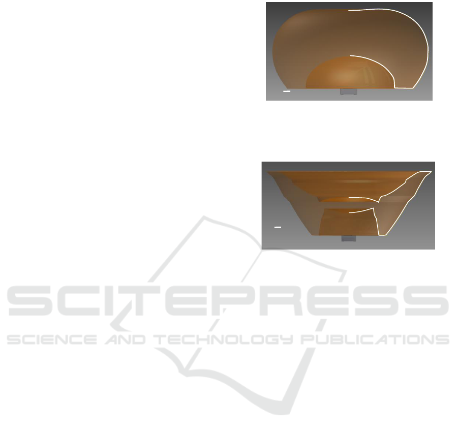
Figure 3: Transmitter optic based on refraction. The body is
formed by rotating the white spline around the optical axis.
It is 22 mm in diameter, 12 mm in height and forms a FOV
with a half-angle of 37°.
Figure 4: Transmitter optic based on refraction and TIR.
The body is formed by rotating the white spline around the
optical axis. It forms a FOV with half-angle of 17°. The
optics diameter is 25 mm and its height is 10 mm.
4.1.2 Results and Discussion
The following considerations stick to the anticipated
FOV with half-angle of 17°. Therefore, only the TIR
optic in Figure 4 is considered. Figure 5 shows the
irradiance at 1 m distance. We get
and
W/cm² which results in
. In comparison to the SFH4451 LED
without additional optics this is an improvement by a
factor of 3.98 (5.99 dB). Even compared to the
spherical lens LA1805.1 from Figure 2 E
min
is
increased 2.36 times (3.73 dB).
The simulation shows, that 10.5 % of the emitted
power is lost due to Fresnel reflections. This could be
reduced by depositing an AR coating. However, the
shape of the optic makes it difficult to deposit
homogenous layers. Another 15.5 % of the power
misses the FOV due to the extended source problem.
By scaling up the optic this loss can be reduced.
Moreover, 5% of the “losses” for
result from
inhomogeneity. The white circle in Figure 5 marks the
minimum within the FOV. The ray file of the SFH4451
reveals that this minimum is not caused by the optic,
but by the reflector within the LED package, which is
not fully rotational symmetric.
1 mm
1 mm
PHOTOPTICS 2019 - 7th International Conference on Photonics, Optics and Laser Technology
252
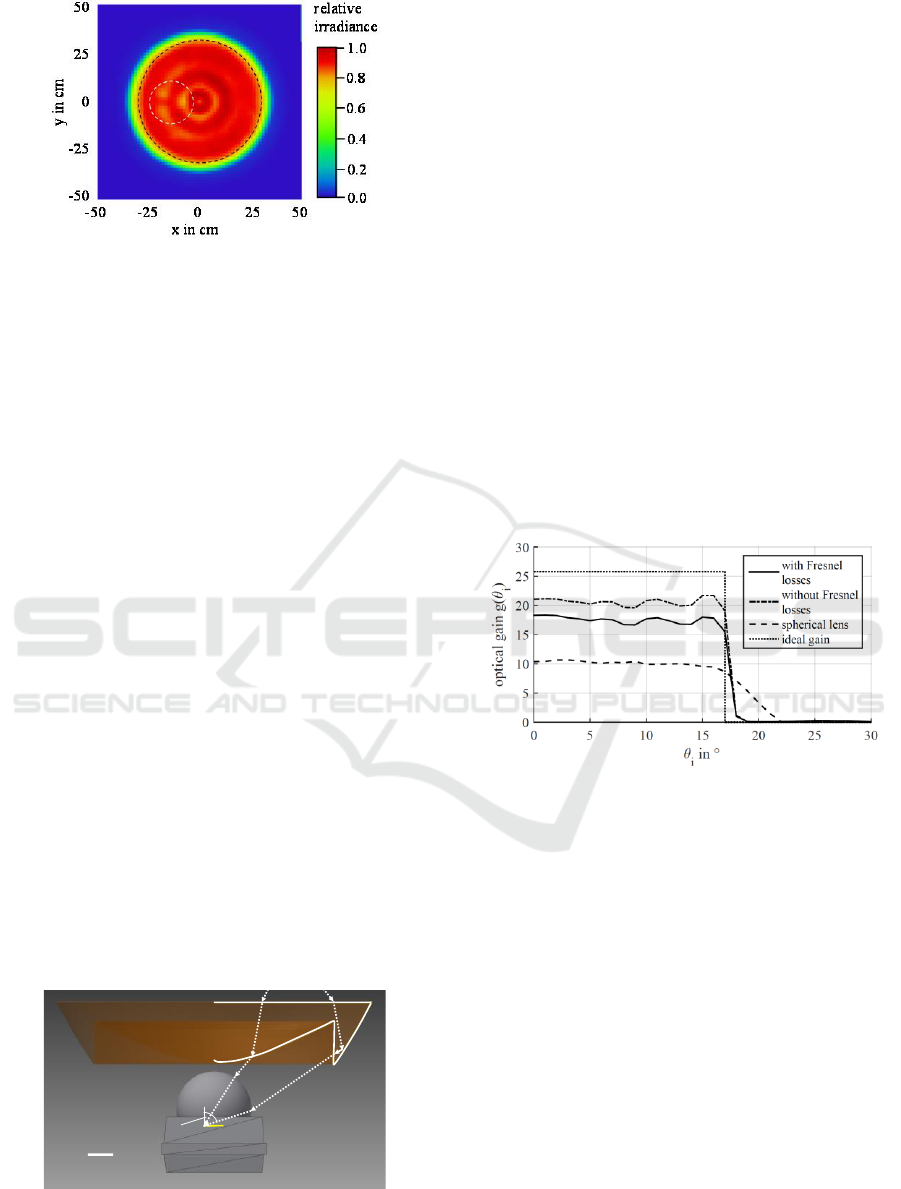
Figure 5: Irradiance in 1 m distance. The black circle marks
the FOV. The white circle highlights minimum.
4.2 Receiver Optics
4.2.1 Design
The Fresnel lens shown in Figure 6 is precisely tailored
to the PD and provides a FOV with a half-angle
. It is 2.5 mm thick and has a refracting section in
the center surrounded by one TIR groove. The
thickness could be further reduced if both sections are
divided into multiple grooves. For the initial design the
edge-ray principle was applied for all surfaces. Due to
the discontinuity between both sections, the edge-ray
principle is not valid for the complete input aperture.
Therefore, the gain is not constant within the FOV. A
homogenization can be achieved by slightly adjusting
the groove for a range of incident angles rather than
only for the maximum incident angle. The designer has
to be aware of shading effects within the grooves for
rays with large incident angles. Due to non-ideal rays
the actual performance at the edge of the FOV will be
worse than one may expect in the first place. These rays
emerge for example from polychromatic light or they
are simply skew rays. The issue can be addressed by
directing the rays not directly the edge of the PD active
area but slightly next to this edge.
For comparison, a second receiver with the
spherical lens LA1074.1 (Thorlabs, 2018) is designed,
as depicted in Figure 1b. The lens has a diameter of
12.7 mm and the distance d to the PD is 2 mm.
Figure 6: Freeform Fresnel lens tailored to PD S10784. The
lens is 12.5 mm in diameter and 2.5 mm in height. The cross
sectional spline is colored white and the active area yellow.
4.2.2 Results and Discussion
Figure 7 shows the gain over the angle of incidence
.
The gain of the Fresnel lens is 15.5. This is 1.8 times
(2.6 dB) higher than the gain of the spherical lens,
which is 8.5. Moreover, the gain of the Fresnel lens
drops much faster the outside FOV. This effectively
reduces inter-channel interference and shot noise
induced by ambient light. According to Figure 7, 15 %
of the power is lost due to Fresnel reflections. These
losses can be reduced by applying an AR coating at
least at the flat top surface of the lens. Despite the
Fresnel losses, the minimum gain g
min
is still about 25
% below the ideal gain g
max
. Three reasons for that can
be derived from the design procedure. First, the
freeform lens directs the rays onto the spherical lens.
The maximum coupling angle
to the active chip is
only 73.5° instead of the ideal 90°. Second, the rays are
not directed directly on to the chip edge, but slightly
next to it. Therefore, the calculated lens is smaller and
thus its gain is lower than g
max
. Third, due to the
discontinuity, the edge-ray principle is not fully
satisfied and losses occur.
Figure 7: Optical gain g of the Fresnel lens and the spherical
lens LA1074.1 in conjunction with PD S10784 over angle
of incidence
. The ideal gain was calculated with
equation 2 assuming
,
,
and
.
4.3 Complete Optical Channel
Figure 8 shows the incident optical power onto the PD
active area P
pd opt
over the FOV for transceivers without
optics, with spherical lenses and with the freeform
lenses from section 4. The freeform lenses provide a
homogenous signal level within the FOV. It varies only
about 1.3 dB and never drops below -24.1 dBm. In
contrast, the signal level provided by the spherical
lenses fluctuates by 7.5 dB and drops at the edge to -
30 dBm. This inhomogeneity is caused by the spherical
transmitter lens. The simulation without any optics
show signal levels down to -36.1dBm. This simulation
is noisy, because only a small amount of rays hit the
detector and the initial number of rays is limited by the
1 mm
Introducing Advanced Freeform Optic Design to Li-Fi Technology
253
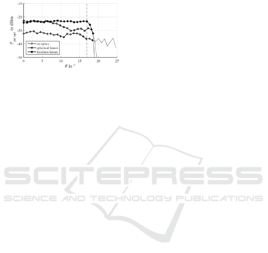
ray file.
Figure 8: Incident optical power
onto the PD active
area over FOV for no optics, spherical lenses (LA1805.1,
LA1074.1) and freeform lenses. The angle corresponds to
a misalignment of both transceivers in the plane over a
distance of 50 cm. The graphs are very noisy in the dotted
region, because only a few rays hit the PD surface.
5 CONCLUSIONS
This paper demonstrates the potential of modern
freeform optics for Li-Fi technology. Design strategies
for transmitter optics are discussed and a TIR based
optic is presented and characterized. The design
example proofs that composite ray mapping is an
efficient tool for shaping homogenous emission
profiles. For the receiver, the designer should tailor the
optic precisely to the PD. A Fresnel lens based on
refraction and TIR is proposed and it is shown that the
optical gain is about 2.6 dB higher compared to a
conventional spherical lens for the considered PD.
We show that the proposed freeform optics provide
a minimum signal level which is 5.9 dB higher than a
optic setup with spherical lenses. The signal level has
an excellent homogeneity within the FOV and
fluctuates only by 1.3 dB. This is about 6.2 dB less
compared to the proposed spherical lenses. This high
homogeneity maximizes the dynamic range and the
sharp cut-off at the edge of the FOV effectively reduces
inter-channel interference and noise.
Our next steps will include the fabrication and
experimental characterization of the designs. Finally,
transmitter and receiver optics should be combined to
one hybrid optic module for size and cost reduction.
REFERENCES
Barry, J. R., 1994. Wireless Infrared Communications. In The
Springer International Series in Engineering and
Computer Science, 1
st
ed., Springer US, 181, 265-289.
Benitez, P. G., Miñano, J.C., et al., July 1, 2004,
Simultaneous multiple surface optical design method in three
dimensions. In Optical Engineering, vol. 43, no. 7, 1489–
1502.
Caves, J., 2016. Introduction to Nonimaging Optics.
2
nd
Edition, CRC Press, 259-319.
Collins, St., O’Brien, D. C., Watt, A., 2014. High gain, wide
field of view concentrators for optical communications.
In Optics Letters vol. 39, no. 7, 1756-1759.
Dross, O. et al., 2004, Review of SMS Design Methods and
Real World Applications. In Proceedings of SPIE 5529 -
The International Society for Optical Engineering.
Ferreira, R. X. G. et al. Oct 1, 2016, High Bandwidth GaN-
Based Micro-LEDs for Multi-Gb/s Visible Light
Communications. In IEEE Photonics Technology
Letters, vol. 28, no. 19, 2023-2026.
Hamamatsu Photonics, May 2013. S 10784. Datasheet.
Islim, M. S., Haas, H., 2016. Modulation Techniques for
Li⁃Fi. In ZTE Communications, vol. 14, no. 2, 29-40.
Koshel, R. J., 2013. Illumination Engineering: Design of
Nonimaging Optics. Wiley-IEEE Press, 17,190,199.
Ma, D., 2015. Exploration of Ray Mapping Methodology in
Freeform Optics, The University of Arizona, 38, 61,
66-95.
Michaelis, D., et al. 2011. Cartesian oval representation of
freeform optics in illumination systems, in Optical
Letters, 36(6), Optical Society of America, 918-920.
Miñano, J.C. et al, 2013. SMS 3D Design Method, Chapter 4
in Illumination Engineering: Design of Nonimaging
Optics. Wiley-IEEE Press, 102.
Osram Opto Semiconductors, 26.06.2016. SFH 4451.
Datasheet, ver. 1.6.
Piegl, L., Tiller, W., J., 1995. The NURBS Book, Springer.
Berlin-Heidelberg, 2
nd
Edition.
Rappaport, T. S. et al. May 10, 2013. Millimeter Wave
Mobile Communications for 5G Cellular: It Will Work!.
In IEEE Access, 1 (2013), 335-349.
Ries, H., Muschaweck, J., April, 2002, Tailored freeform
optical surfaces. In Journal of the Optical Society of
America A, 19(3):590-5, Optical Society of America.
Shen, S. C., et al., 2013. A Novel TIR-R Concentration
Module of Uniformly Solar Energy for HCPV Systems.
In Proceedings of the 2013 IEEE/SICE International
Symposium on System Integration, Kobe, 747-752.
Thorlabs, LA1074,[online]www.thorlabs.com, 12.11.2018.
Thorlabs, LA1805,[online]www.thorlabs.com, 12.11.2018.
Wallhead, I., et al. 2012. Design of an efficient Fresnel-type
lens utilizing double total internal reflection for solar
energy collection, in Optics Express, vol. 20, no. S6,
Optical Society of America.
Wang, K., Liu, S., Xiaobing, L. Wu, D., September 2017.
Freeform Optics for LED Packages and Applications,
Wiley, 1
st
Edition, 25, 53-54, 58-60.
Welford, W. T., Winston, R., 1989. High Collection
Nonimaging Optics, Academic Press Inc., San Diego, 1
st
Edition, 21-22, 54.
Winston, R., Miñano, J.C., Benitez, P. G., 2015. Non-
imaging Optics. Elsevier Academic Press,181-217.
Wu, X. , Safari, M., Haas, H., 2017. Access Point Selection
for Hybrid Li-Fi and Wi-Fi Networks, in IEEE , Tran-
sactions on Communications, vol. 65, no. 12, 5375-5383
PHOTOPTICS 2019 - 7th International Conference on Photonics, Optics and Laser Technology
254
