
Formation of Low Resistance Contacts to p-type 4H-SiC
using Al-Film Source Laser Doping
Kento Okamoto
1
, Toshifumi Kikuchi
1
, Akihiro Ikeda
2
, Hiroshi Ikenoue
1
and Tanemasa Asano
1
1
Graduate School of Information Science and Electrical Engineering, Kyushu University, 744 Motooka,
Nishi-ku, Fukuoka, Japan
2
Department of Computer and Information Sciences, Sojo University, 4-22-1 Ikeda, Nishi-ku, Kumamoto, Japan
{okamoto@fed., asano@}ed.kyushu-u.ac.jp
Keywords: 4H-SiC, Ohmic Contact, Laser Doping, Specific Contact Resistance, Aluminum, p-type, Ti/Al.
Abstract: Impact of laser doping on the formation of ohmic contacts to 4H-SiC has been investigated. The laser doping
was performed by irradiating pulse-width stretched KrF excimer laser to an Al film coated on the surface of
4H-SiC. Doping and contact formation on the carbon face of 4H-SiC were investigated. The doping was
carried out while keeping the sample at room temperature. It is found that the laser doping is able to introduce
Al up to a concentration as high as 5×10
21
cm
-3
. As a result of heavy doping, the contact made of Ti/Al
metallization provides the ohmic contact whose specific contact resistance as low as 4.0×10
-6
Ωcm
2
without
additional heat treatment. The specific contact resistance is lower than that reported for ohmic contacts formed
by using ion implantation.
1 INTRODUCTION
The electric power consumption is expected to
increase significantly, due to the rise of electric
vehicles and artificial intelligence. Development of
low-loss power devices is, therefore, highly
demanded. Although silicon (Si) power devices have
been mainstream, they are facing the physical limit of
Si. Wide-gap semiconductors such as silicon carbide
(SiC) and gallium nitride are attracting great attention
for next-generation power devices.
4H-SiC (hexagonal silicon carbide) has the figure
of merit due to its superior physical properties such as
high breakdown voltage, excellent thermal
conductivity, and high saturation drift-velocity of
electrons. Therefore, it is regarded as one of the most
promising materials of power devices. Processing
technology of 4H-SiC devices has been well
advanced as they become of practical use. However,
the formation of low resistance contacts to 4H-SiC
remains as a challenge. Because the bandgap of 4H-
SiC is much wider than that of Si, the potential barrier
becomes large at the interface between the metal and
the semiconductor and, consequently, the carriers
(electrons and holes) hardly flows across the
interface. On the other hand, devices made of 4H-SiC
such as insulated gate bipolar transistors (IGBTs) are
expected to carry a much higher current than those
made of Si (Usman and Nawaz, 2014). Therefore,
very-low resistance contacts are highly demanded.
To reduce the ohmic contact resistance, reduction
of the barrier height at the metal/semiconductor
interface and/or an increase in doping concentration
near the semiconductor surface is needed. Reduction
of barrier height suffers from the constraint of metal
work function. p-type heavy-doping of 4H-SiC has
remained as one which we should develop since the
acceptor energy level is extremely large (0.29 eV for
B and 0.18 eV for Al) and, therefore, the activation
ratio is small. Ion implantation is widely used as the
doping method to form a heavily doped layer at the
semiconductor surface (Frazzetto et al., 2011).
However, it requires high temperature annealing at
about 1700ºC to activate the implanted dopant atoms
(Ito, Tsukimoto and Murakami, 2006). This high
temperature annealing induces undesirable
phenomena such as generation of 3C polytype crystal
structure and deterioration in yield. Therefore, low-
temperature processing is preferred. Low temperature
processing is also mandatory to form ohmic contacts
to the back side of the wafer where the device active
region has fabricated on the front side.
We have shown that a heavily doped layer can be
formed by laser irradiation to an Al film deposited on
the 4H-SiC surface. A generation of Al plasma during
294
Okamoto, K., Kikuchi, T., Ikeda, A., Ikenoue, H. and Asano, T.
Formation of Low Resistance Contacts to p-type 4H-SiC using Al-Film Source Laser Doping.
DOI: 10.5220/0007583002940298
In Proceedings of the 7th International Conference on Photonics, Optics and Laser Technology (PHOTOPTICS 2019), pages 294-298
ISBN: 978-989-758-364-3
Copyright
c
2019 by SCITEPRESS – Science and Technology Publications, Lda. All rights reserved
laser irradiation was observed by using optical
emission spectroscopy (Ikeda et al., 2016). We
suppose that high temperature molten Al is formed on
the 4H-SiC surface by laser irradiation and it acts as
the dopant source and also as the heat reservoir.
In this paper, we show that very-low resistance
contacts can be formed by using the laser doping with
an Al film, which does not require high temperature
annealing. The carbon-face (C-face) of 4H-SiC is
used in the investigation since this face composes the
back side of conventional MOS-gated devices.
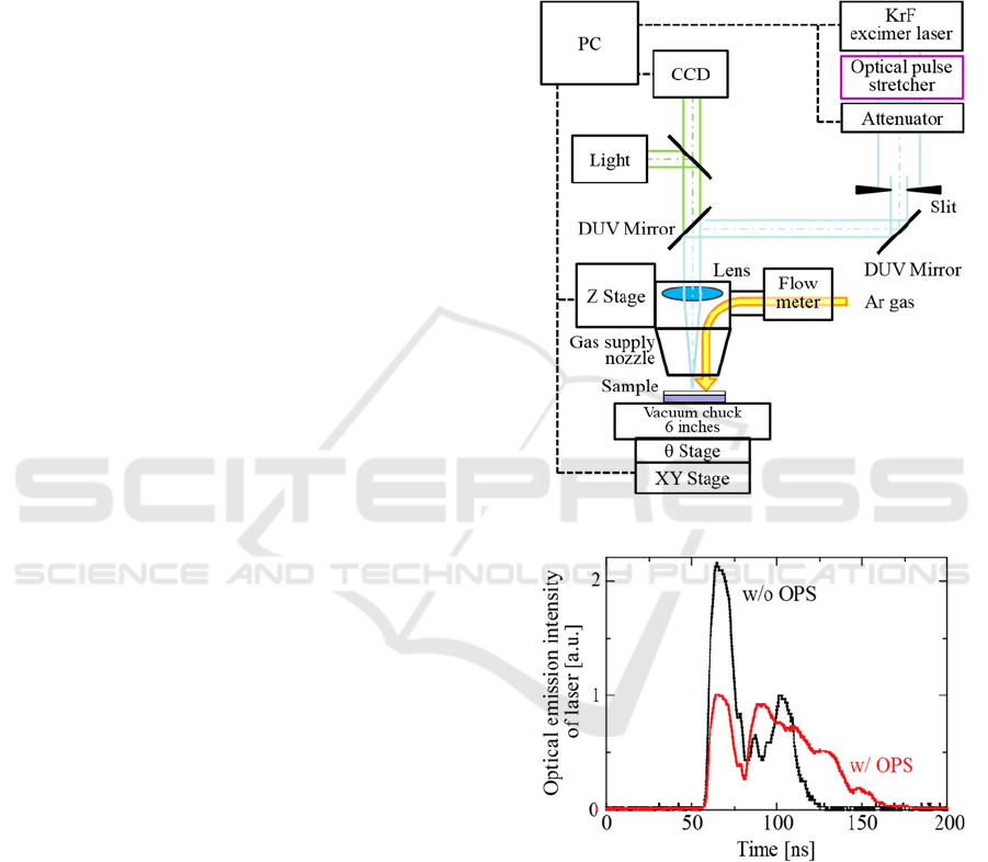
2 EXPERIMENTAL
A non-doped semi-insulating 4H-SiC substrate was
adopted in order to avoid the wraparound current at
the time of measurement. The experimental setup
used was schematically shown in Fig. 1. An Al thin
film (120 nm thick) was deposited on the C-face of
the substrate by DC magnetron sputtering. The Al-
coated 4H-SiC chip was chucked with a vacuum
pump to a computer-controlled mechanical scanning
stage and the KrF excimer laser (wavelength: 248
nm) was irradiated while scanning the stage. The laser
irradiation condition was as follows; fluence: 2-4
J/cm
2
, number of laser pulses: 1-36 shots, and
frequency: 100 Hz. The laser spot size was adjusted
with a slit to be ~300 µm in the direction
perpendicular to the scanning direction while the slit
was open along the scanning direction. The original
laser pulse was expanded by using an optical pulse
stretcher (OPS) to suppress laser ablation of the
surface and to increase the heat retention time by laser
irradiation (See Fig. 2) (Ikeda et al., 2017). Ar gas
blowing to the sample surface was employed to keep
the surface unreacted during irradiation. After the
laser irradiation, the Al film remained in the irradiated
area as well as the unirradiated area was etched with
phosphoric acid. The Al etching was followed by CF
4
plasma and O
2
plasma etchings to remove Si and C
based materials produced at the surface by the laser
irradiation. The CF
4
plasma etching condition was as
follows; the pressure was 30 Pa, the etching time was
10 min, and the discharge power was 100 W. The O
2
plasma etching condition was as follows; the pressure
was 100 Pa, the etching time was 5 min, and the
discharge power was 400 W. Furthermore, the oxide
film at the surface was etched with buffered
hydrofluoric acid (BHF, 6%). The above cleaning
processes by plasma and BHF were repeated several
times. A 100 nm-thick Ti film and a 400 nm-thick Al
film were sequentially deposited on the treated
surface by using a sputtering system to form a metal
contact of Al/Ti/p-SiC structure. The Ti/Al electrode
is one of the promising contact metals to p-type SiC
(Crofton et al., 2002), (Ito, Tsukimoto and Murakami,
2006). The deposited metal electrode was patterned
by using photolithography. The electrode size is 400
× 100 µm. Five sets of test patterns whose electrode
spacing was modulated were prepared on a test chip.
Figure 1: Schematic of the experimental setup.
Figure 2: Waveforms of laser pulse intensity produced with
and without optical pulse stretcher (OPS).
The sample surface was observed with a scanning
electron microscope (SEM). The current-voltage (I-
V) characteristic was evaluated by a semiconductor
parameter analyzer, Agilent 4156C. The depth profile
of aluminum from the doped layer surface was
obtained by secondary ion mass spectrometry
(SIMS). The specific contact resistance was evaluated
by the transfer length method (TLM) based on a
transmission line model (Crofton et al., 2002).
Formation of Low Resistance Contacts to p-type 4H-SiC using Al-Film Source Laser Doping
295
3 RESULTS AND DISCUSSION
3.1 Al Doping
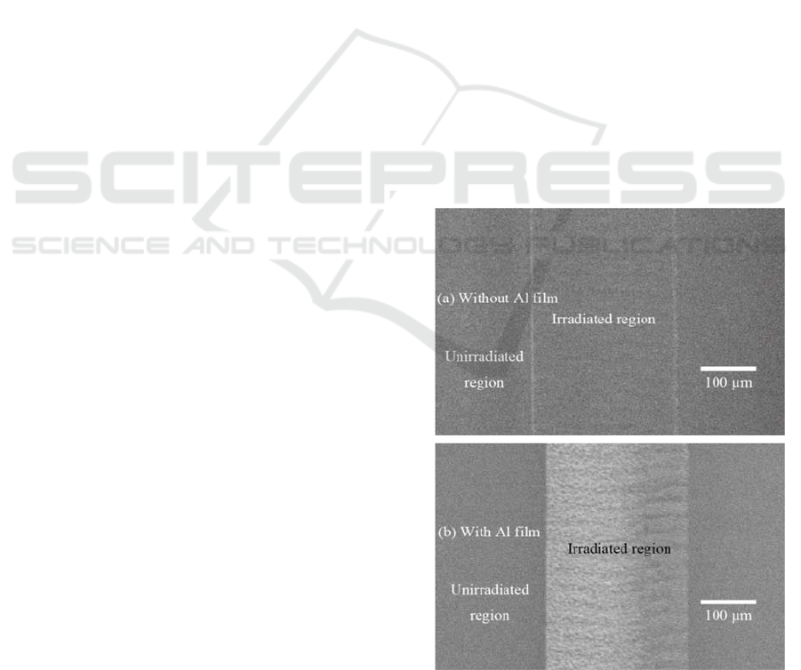
Figures 3(a) and 3(b) show the SEM images of the
sample surfaces irradiated without and with the Al
film, respectively. The laser scanned area of the
sample irradiated with the Al film (Fig. 3(b)) shows a
brighter contrast than the other areas, while the laser
scanned area in the sample without the Al films (Fig.
3(a)) shows a similar brightness to the other areas.
Since the potential increase due to p-type formation
results in the enhanced emission of secondary
electrons in SEM, these results indicate that p-type
doping of 4H-SiC can be performed by the laser
irradiation to an Al film deposited on the 4H-SiC
substrate.
In order to verify the doping of Al, the presence
of Al in 4H-SiC and depth distribution were measured
by using SIMS. Figure 4 shows the depth profiles of
Al concentration obtained by laser doping at 3.4 J/cm
2
with 4 shots. We find that Al as high as 5×10
21
cm
-3
in concentration is introduced by the laser doping. In
the figure, the depth profile of Al ion-implanted at 40
keV to a dose of 5.0 ×10
14
cm
-2
was also plotted as a
reference. The profile of implanted Al well agrees
with the theoretical prediction, which indicates that
the SIMS measurement gives accurate concentration
and profile of Al. We find from a comparison of the
two profiles shown in Fig. 4 that the laser doping
produces a highly Al-doped layer particularly in the
vicinity of the surface.
3.2 Electrical Characteristics
Figure 5 shows the change in I-V characteristic
between two electrodes formed on the samples with
and without laser irradiation. The gap spacing
between the electrodes was about 30 µm. The probe
voltage was swept from -2 to 2 V. In the sample
without laser irradiation, the current hardly flows.
The current value was several pA at the maximum.
On the other hand, in the sample with laser irradiation
using the Al thin film, current up to several mA flows,
which indicates that the resistance markedly
decreased in the laser irradiated region. Besides, the
I-V curve shows a good linear relation, suggesting
that a highly doped p-type layer was formed by the
laser doping.
Figure 6 shows the total resistance (R
T
) between
two electrodes as a function of the
spacing
length
(L)
between the two electrodes. R
T
was calculated from
the slope of the I-V characteristic from which a linear
relation
was
obtained.
In
order
to
accurately
derive
the specific contact resistance, TLM characteristic
shown in Fig. 6 was adopted. From the TLM
characteristics, an effective transfer length (L
T
) and
contact resistance (R
C
) can be obtained from the x-, y-
intercept of straight line approximated from the plot,
respectively. L
T
corresponds to the distance at which
the voltage or current attenuates to 1/e. The specific
contact resistance (ρ
C
) is derived by multiplying R
C
,
L
T
, and the width (W) of the doping region:
.
(1)
From the experimental results, ρ
C
is evaluated to be
approximately 4.0×10
-6
Ωcm
2
. This value is
significantly lower than the value of the contact
resistance obtained by the ion implantation method as
follows. In case of Ti/Al contacts to p-type 4H-SiC
doped to a concentration of ~10
19
cm
-3
, ρ
C
=2×10
-3
-
8×10
-4
Ωcm
2
(Ito, Tsukimoto and Murakami, 2006). In
case of Ti/Al/Ni contact to p-type 4H-SiC doped to a
concentration of 10
20
cm
-3
, ρ
C
=2.3×10
-4
Ωcm
2
(Vivona
et al., 2017). In case of Ni/Al contacts to p-type 4H-
SiC doped to a concentration of 10
19
cm
-3
, ρ
C
= 3×10
-5
-
8×10
-6
Ωcm
2
(Vang et al., 2006). In addition, high-
temperature post-deposition annealing (PDA) at about
1000°C is usually required to form a good ohmic
contact on 4H-SiC. The PDA causes chemical
reactions between 4H-SiC and the metals at the
interface to form silicide and carbide alloys.
Figure 3: SEM images of the surfaces of SiC samples (a)
irradiated without the Al film and (b) irradiated with the Al
film.
PHOTOPTICS 2019 - 7th International Conference on Photonics, Optics and Laser Technology
296
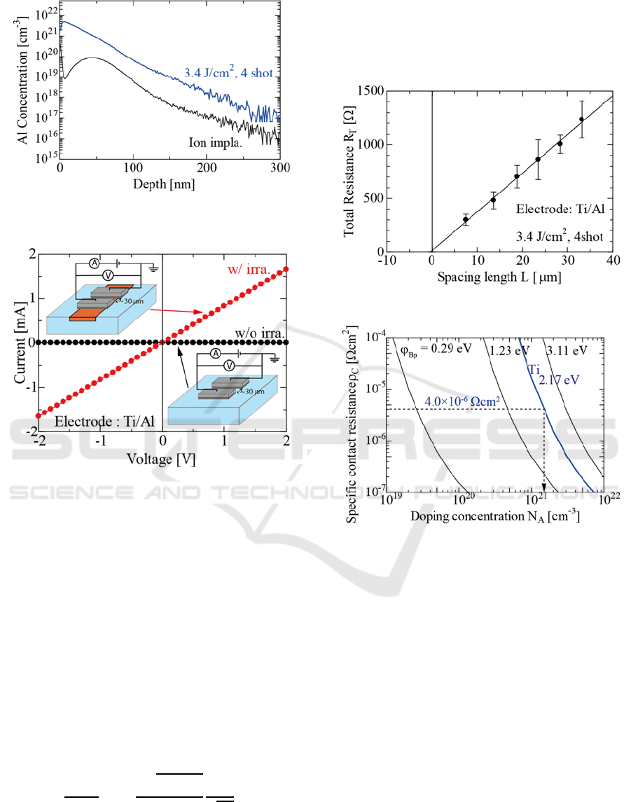
Figure 4: Depth profiles of Al introduced in 4H-SiC by
using laser doping and ion implantation.
Figure 5: Change in I-V characteristic between the
electrodes formed on samples with and without laser
irradiation.
3.3 Theoretical Consideration
Specific contact resistance is a function of the
potential barrier height at the interface. In addition, it
is known that the specific contact resistance strongly
depends on the doping concentration and is reduced
with the increase of doping concentration. In a contact
of very heavily doped semiconductor, the flow of
carriers across the interface is dominated by the field
emission (FE). That is, for N
A
≥10
19
cm
-3
, ρ
C
is
dominated by the tunneling process and decrease
rapidly with increased doping. Theoretical analysis of
FE gives the specific contact resistance described by
the following equation: (Sze, 2007)
∗∗
exp
2
∗
ħ
√
(2)
where k is the Boltzmann constant, q is the
elementary charge, A
**
is the effective Richardson
constant, T is the absolute temperature,
is the
permittivity of 4H-SiC (Saito et al., 2004),
∗
is the
effective mass of the light hole (Lindefelt, 1998),
is barrier height, ħ is the reduced Planck constant, and
N
A
is the doping concentration of acceptor.
Figure 6: Resistance values of a TLM pattern.
Figure 7: Doping concentration dependence of specific
contact resistance calculated for various barrier height.
Figure 7 shows the doping concentration
dependence of specific contact resistance calculated
from Eq. (2) for various barrier height. The barrier
height calculated from the work function of Ti (4.33
eV) (Huang et al., 2012) and the electron affinity of
4H-SiC is 2.17 eV. The specific contact resistance
calculated for this value is shown by the solid line in
Fig. 7. The theory suggests that doping concentration
of about 10
21
cm
-3
is required to obtain 4.0×10
-6
Ωcm
2
.
This doping concentration agrees with experimental
results of SIMS shown in Fig. 4.
4 CONCLUSIONS
We have investigated the formation of low resistance
p-type contacts by using laser doping with Al thin
film as the source on the C-face of 4H-SiC. Al doping
Formation of Low Resistance Contacts to p-type 4H-SiC using Al-Film Source Laser Doping
297

to the concentration as high as 5×10
21
cm
-3
can be
performed
by the irradiation of pulsed excimer laser
to the Al film coated 4H-SiC sample kept at room
temperature. Owing to the heavy doping, the contact
made of Ti/Al metallization provides an ohmic
contact whose specific contact resistance as low as
4.0×10
-6
Ωcm
2
without additional heat treatment.
This specific contact resistance is lower than that
reported for ohmic contacts formed by using ion
implantation. Thus the laser doping with Al thin-film
source is a promising candidate to form low
resistance ohmic contacts of 4H-SiC power devices.
ACKNOWLEDGEMENTS
This work is supported in part by Grants-in-Aid for
Scientific Research, KAKENHI, (No. JP17K06387
and No. JP16H02342) from Japan Society for the
Promotion of Science. A part of this work was carried
out by using the facility of Department of Gigaphoton
Next GLP.
REFERENCES
Crofton, J. et al., 2002. ‘Finding the optimum Al–Ti alloy
composition for use as an ohmic contact to p-type SiC’,
Solid-State Electronics. Pergamon, 46, pp. 109–113.
Frazzetto, A. et al., 2011. ‘Structural and transport
properties in alloyed Ti/Al Ohmic contacts formed on
p-type Al-implanted 4H-SiC annealed at high
temperature’, Journal of Physics D: Applied Physics,
44.
Huang, L. et al., 2012. ‘Low resistance Ti Ohmic contacts
to 4H-SiC by reducing barrier heights without high
temperature annealing’, Applied Physics Letters, 100,
pp. 1–5.
Ikeda, A. et al., 2017. ‘Increased doping depth of Al in wet-
chemical laser doping of 4H-SiC by expanding laser
pulse’, Materials Science in Semiconductor Processing.
Elsevier Ltd, 70, pp. 193–196.
Ikeda, A. et al., 2016. ‘Al doping of 4H-SiC by laser
irradiation to coated Al film and its application to
junction barrier Schottky diode’, Japanese Journal of
Applied Physics, 55.
Ito, K., Tsukimoto, S. and Murakami, M., 2006. ‘Effects of
Al ion implantation to 4H-SiC on the specific contact
resistance of TiAl-based contact materials’, Science
and Technology of Advanced Materials, 7, pp. 496–
501.
Lindefelt, U., 1998. ‘Doping-induced band edge
displacements and band gap narrowing in 3C–, 4H–,
6H–SiC, and Si’, Journal of Applied Physics, 84, pp.
2628–2637.
Saito, W. et al., 2004. ‘Theoretical limit estimation of
lateral wide band-gap semiconductor power-switching
device’, Solid-State Electronics, 48, pp. 1555–1562.
Usman, M. and Nawaz, M., 2014. ‘Device design
assessment of 4H-SiC n-IGBT - A simulation study’,
Solid-State Electronics. Elsevier Ltd, 92, pp. 5–11.
Vang, H. et al., 2006. ‘Ni-Al ohmic contact to p-type 4H-
SiC’, Superlattices and Microstructures, 40, pp. 626–
631.
Vivona, M. et al., 2017. ‘Electrical and structural properties
of surfaces and interfaces in Ti/Al/Ni Ohmic contacts
to p-type implanted 4H-SiC’, Applied Surface Science.
Elsevier B.V., 420, pp. 331–335.
Sze, S., 2007. Physics of Semiconductor Devices, Jhon
Wiley and Sons, Inc., Hoboken, New Jersey, 3
nd
edition.
PHOTOPTICS 2019 - 7th International Conference on Photonics, Optics and Laser Technology
298
