
25 Gb/s NRZ and 50 Gb/s PAM-4 Transimpedance Amplifier with
Active Feedback and Equalization in 90 nm CMOS Technology
Hao-Wen Hsu, Chih-Chen Peng, Jau-Ji Jou, Tien-Tsorng Shih, Yaw-Dung Wu, Shao-I Chu,
Chih-Yuan Lien and Bing-Hong Liu
Department of Electronics Engineering, National Kaohsiung University of Science and Technology,
No. 415, Jiangong Rd., Sanmin Dist., Kaohsiung City 80778, Taiwan
Keywords: Transimpedance Amplifier (TIA), Active Feedback, Equalizer, Four-level Pulse Amplitude Modulation
(PAM-4).
Abstract: In this paper, a high-linearity transimpedance amplifier (TIA) was designed in 90 nm CMOS technology.
The input stage of the TIA was a regulated cascade circuit for low input impedance. The active feedback
structure was used to replace the feedback resistor and to reduce the chip size. An equalizer was also used in
the TIA to compensate the high-frequency response. Within input current amplitude of 1.1 mA, the total
harmonic distortion of the TIA can be below 5%. The bandwidth of the TIA was about 26 GHz and its
input-referred current density was below 74 pA/√Hz within the bandwidth. The TIA can be applied in 25
Gb/s non-return zero (NRZ) and 50 Gb/s (25 Gbaud) four-level pulse amplitude modulation (PAM-4)
optical receivers. The power dissipation of the chip is 11.6 mW and the chip area is 0.151 mm
2
.
1 INTRODUCTION
Since the advent of optical fiber transmissions, the
data transmission speed is increasing in recent years
and is widely used in local area networks, regional
networks, and data centers. Therefore, more people
have invested in the research and promotion of high-
speed fiber optic circuit design. The multi-level
modulation signals can reduce the channel symbol
rate and the circuit bandwidth, so the high-speed
circuit for optical communications can be designed
easier. In the same transmission bandwidth, the data
bit rate of the 4-level pulse amplitude modulation
(PAM-4) signal can be doubled than the non-return
to zero (NRZ) signal (Szczerba, 2012). Therefore,
the PAM-4 signal is defined as a kind of the standard
signal formats in the 200 and 400 Gb/s Ethernets
(Bhoja, 2017; Baveja, 2018). Using eight channels
that operate at 25 Gb/s NRZ or 50 Gb/s PAM-4, the
200 Gb/s or 400 Gb/s transceiver modules can be
achieved.
In the optical receiver module, the
transimpedance amplifier (TIA) and the main
amplifier are usually used. If the nonlinear distortions
can be tolerated, the limiting amplifier (LA) can
become the main amplifier. However, the distortion
of the PAM-4 signal is highly dependent on the
linearity of transmission and circuit. The LA can
introduce nonlinear distortions and will degrade the
PAM-4 signal quality. Therefore, in the PAM-4
optical receiver, the high-linearity TIA will be
needed and the LA cannot be used. The 100 Gb/s
PAM-4 linear TIA was designed in 16 nm FinFET
CMOS process (Lakshmikumar, 2018), and the low-
noise high-linearity 56 Gb/s PAM-4 optical receiver
was designed in 45 nm SOI CMOS technology (Xie,
2018). Our TIA circuit was designed in 90 nm
CMOS technology, so the bandwidth compensation
skills were needed for the high-speed TIA (Salhi,
2017; Hiratsuka, 2018). Therefore, an equalizer (EQ)
circuit was added in our inductor-less TIA. In this
paper, a high- linearity TIA with an EQ is designed
in 90 nm CMOS technology for 25 Gb/s NRZ and 50
Gb/s PAM-4 transmissions.
2 CIRCUIT ARCHITECTURE
Figure 1 shows the block diagram of our TIA circuit.
The TIA was designed as a fully differential circuit
structure. A differential circuit can effectively reduce
the noise interference from the power supply or the
Hsu, H., Peng, C., Jou, J., Shih, T., Wu, Y., Chu, S., Lien, C. and Liu, B.
25 Gb/s NRZ and 50 Gb/s PAM-4 Transimpedance Amplifier with Active Feedback and Equalization in 90 nm CMOS Technology.
DOI: 10.5220/0007829102510257
In Proceedings of the 16th International Joint Conference on e-Business and Telecommunications (ICETE 2019), pages 251-257
ISBN: 978-989-758-378-0
Copyright
c
2019 by SCITEPRESS – Science and Technology Publications, Lda. All rights reserved
251
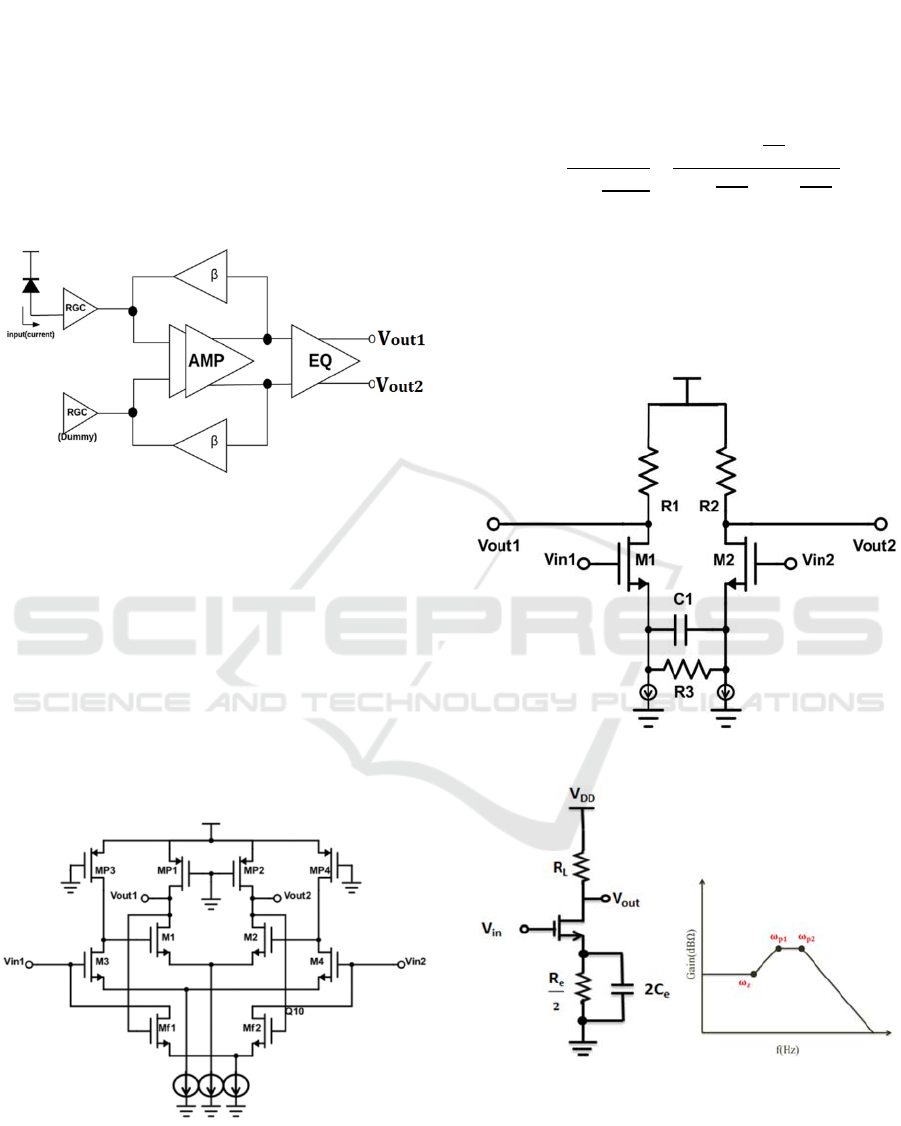
substrate, and can increase the voltage swing. In
addition, the nonlinear distortion and even-order
harmonics can be also reduced. The input stage of the
TIA used a regulated cascade (RGC) circuit (Seng,
2013). The RGC circuit has a low input resistance to
suitable to be an input stage for current signals. In the
TIA, the active negative feedback was used to
replace the feedback resistor, and the voltage output
of the TIA is not resistively load by the feedback
device.
Figure 1: Block diagram of our TIA with active feedback
and equalization.
Figure 2 shows the schematic diagram of the TIA
with active feedback, not including the RGC input
stages. The TIA is a two-stage differential amplifier,
the M3 and M4 is a differential pair, and the M1 and
M2 is another differential pair. The feedback paths
are from the drains of the M1 and M2 to the gates of
the M3 and M4. The feedback devices use the
voltage-controlled current sources, Mf1 and Mf2.
For reducing the chip size, the drain loads of the
two-stage differential amplifier use active loads,
MP1, MP2, MP3, and MP4.
Figure 2: Schematic of our TIA with active feedback.
Figure 3 shows the schematic diagram of the
equalizer in the TIA. The equalizer was designed in
the differential configuration with source and
capacitive degenerations (Talluri, 2015). The
equalizer was also the output stage in the TIA, so the
R1 and R2 were set as 50 Ω matching resistors.
Figure 4 shows the half circuit of the equalizer, its
transfer function can be written as
EQs
G
R
1
G
R
2
1
s
1
s
1
s
(1)
where
z
= 1/(R
e
C
e
),
p1
= (1+G
m
R
e
/2)/(R
e
C
e
), and
p2
= 1/(R
L
C
L
). The Bode’s plot of the equalizer is
also shown in Figure 4. The values of R3 and C1 can
be set carefully to compensate for the high-
frequency response of the TIA and to extend the
bandwidth.
Figure 3: Schematic of the equalizer.
Figure 4: Half circuit and frequency response of the
equalizer.
Figure 5 shows the layout diagram of the TIA
circuit with active feedback and equalization. The
TIA chip was designed in TSMC 90 nm CMOS
technology. The chip area including the pads is
0.343 0.44 mm
2
. The input pad can be connected
OPTICS 2019 - 10th International Conference on Optical Communication Systems
252
with a photodiode, the Vout1 and Vout2 pads are the
differential output ends, and the Vbias pad can
adjust the currents of the current source circuits.
There are two voltage source pads, Vdd, and four
ground pads, Gnd, in the TIA chip.
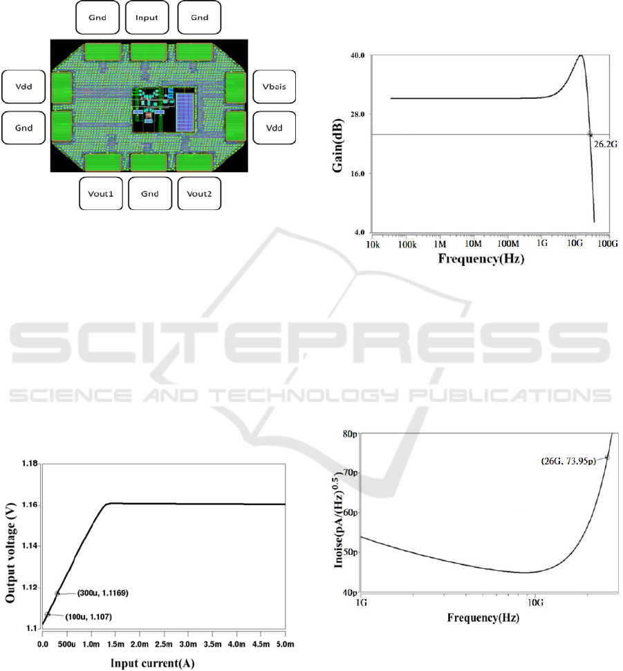
Figure 5: Layout diagram of the TIA chip.
3 RESULTS AND DISCUSSION
3.1 Simulated Results
Figure 6 shows the post-simulated DC transfer curve
of the TIA. By the curve, the transimpedance gain of
34 dBΩ is estimated. For the linear operation, the
peak-to-peak input current must be below 1.1 mA,
while the output swing reaches 80% of the fully
limited value of the TIA. The maximum output
voltage amplitude is about 55 mV.
Figure 6: Post-simulated DC transfer curve of the TIA.
Figure 7 shows the post-simulated frequency
response of the TIA. In the simulations, an
equivalent photodiode circuit was added and the
capacitance and resistance of the equivalent
photodiode were 0.3 pF and 2 kΩ, respectively. For
the lower frequency range, the gain was about 34
dBΩ and correspondent with the estimation for the
DC analysis. There was a peak response at about 12
GHz, and the peak response was caused by the
equalizer. The 3-dB bandwidth of the TIA was about
26 GHz, so the TIA can be suitable for the 25 Gb/s
NRZ and 50 Gb/s PAM-4 operations.
Figure 7: Post-simulated frequency response of the TIA.
The input referred current noise density of the
TIA was simulated, as shown in Figure 8. Within the
bandwidth, the input referred current noise density
was below 74 pA/√Hz. The noise performance of
the TIA is not very excellent. Generally, active
feedback tends to result in more noise than shunt
resistance feedback.
Figure 8: Post-simulated input referred current noise
density of the TIA.
For PAM-4 signals, the linearity of the circuit or
transmission system seriously influences the signal
quality. Therefore, using a 5 GHz input sine-wave
signal, the total harmonic distortion of the TIA versus
the peak-to-peak input current was simulated, as
shown in Figure 9. When the peak-to-peak input
25 Gb/s NRZ and 50 Gb/s PAM-4 Transimpedance Amplifier with Active Feedback and Equalization in 90 nm CMOS Technology
253
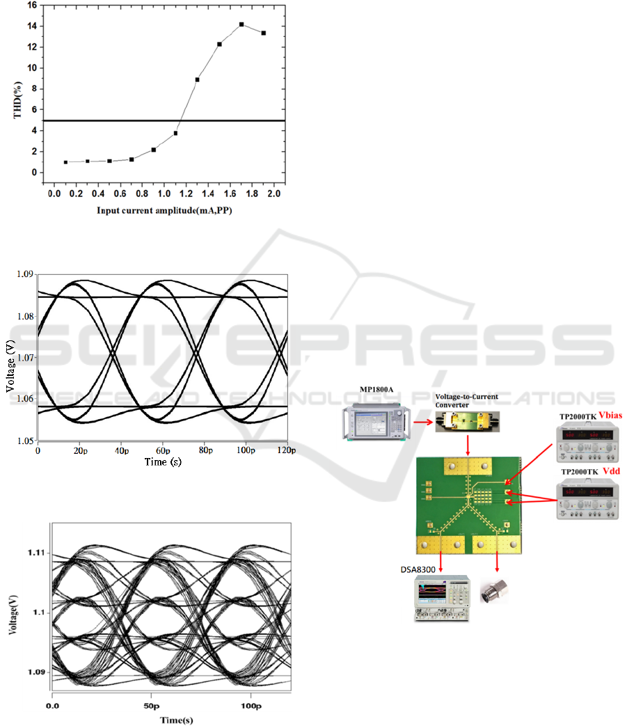
current is below 1.1 mA, the total harmonic
distortion can be below 5%. The linearity of the TIA
is good. The condition for the linear operation was
also correspondent with the evaluation from the DC
transfer curve.
Figure 9: Post-simulated total harmonic distortion of the
TIA.
Figure 10: Post-simulated 25 Gb/s NRZ output voltage eye
diagram of the TIA.
Figure 11: Post-simulated 50 Gb/s PAM-4 output voltage
eye diagram of the TIA.
The 25 Gb/s NRZ and 50 Gb/s (25 Gbaud/s)
PAM-4 output voltage eye diagrams were simulated
for the peak-to-peak input current of 400 μA, as
shown in Figures 10 and 11. The total output voltage
amplitude was above 20 mV. For the 25 Gb/s NRZ
operation, the eye diagram of the TIA output signal is
very clear. For the 50 Gb/s PAM-4 operation, the top,
middle, and bottom eyes of the eye diagram of the
TIA output signal can obtain the same eye-height,
because the linearity of the TIA was good.
3.2 Measured Results
The TIA chip was tested through an evaluation
board. We designed the evaluation board, and the
high-frequency printed circuit board (PCB) material
was Rogers 4350B. The high-frequency signal traces
were designed using grounded coplanar waveguides
on the PCB. To avoid DC level into the wide-
bandwidth oscilloscope, the DC block was used in
the signal output end. In our measurements, the
photodiode (PD) was not used with the TIA chip. A
voltage-to-current converter including a 1 kΩ
resistor and a 0.15 pF capacitor was used to convert
the voltage signal from the arbitrary waveform
generator into the current signal. The 0.15 pF
capacitor was used as the equivalent capacitance of
PD. For the TIA chip testing, the measurement
architecture is shown in Figure 12.
Figure 12: Measurement architecture for the TIA chip on a
PCB.
A 25 Gb/s NRZ electrical eye diagram from the
signal quality analyzer (Anritsu MP 1800A) was
measured through the digital sampling oscilloscope
(Tektronix DSA8300), as shown in Figure 13(a), the
rise and fall times of the eye diagram were 18.2 ps
and 15.1 ps, the peak-to-peak time jitter was 3.54 ps,
OPTICS 2019 - 10th International Conference on Optical Communication Systems
254
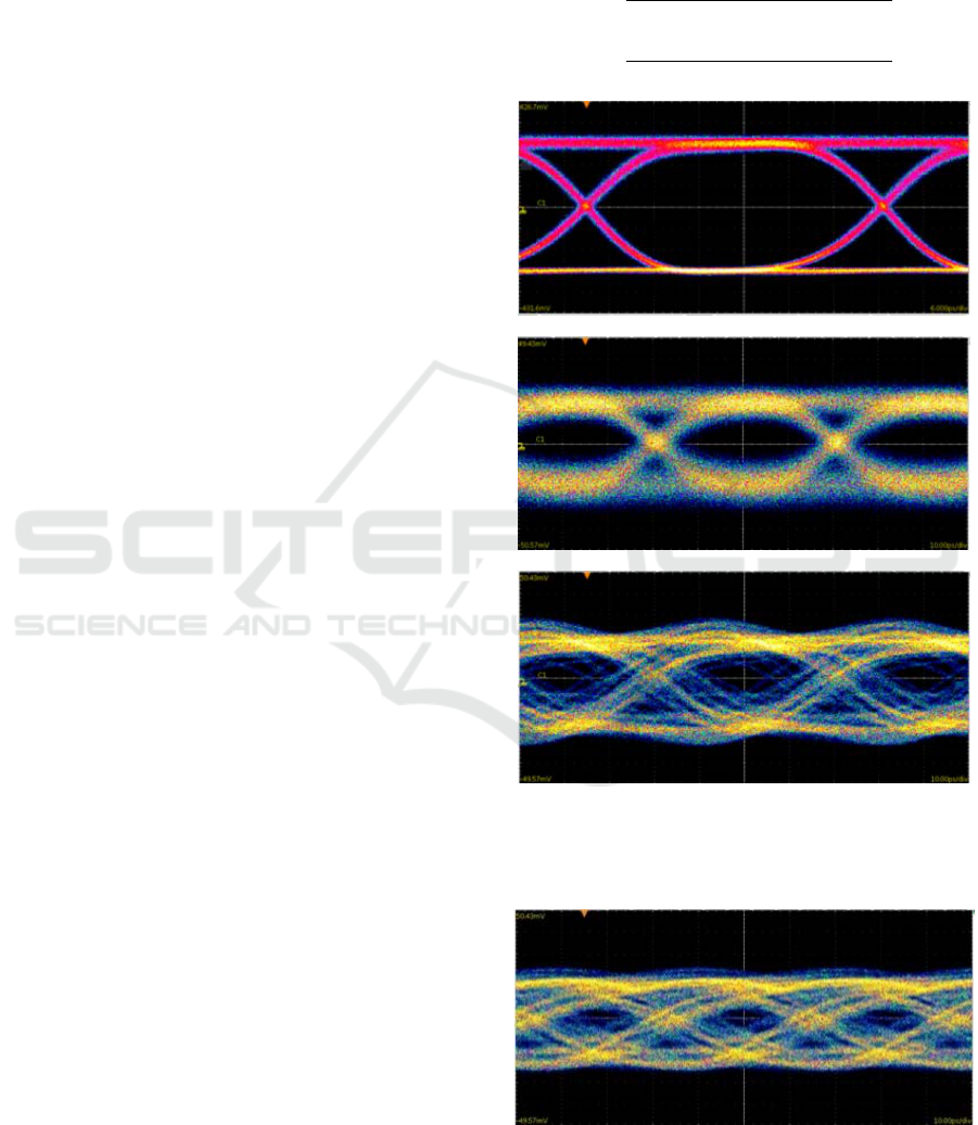
the signal-to-noise ratio (SNR) was 34.3, and the
voltage amplitude was 514.5 mV. From the voltage-
to-current converter, Figure 13(b) shows the 25 Gb/s
NRZ eye diagram with a rise time of 14.3 ps, a fall
time of 12.4 ps, a peak-to-peak time jitter of 17.1 ps,
an SNR of 10.0, and an amplitude of 37.8 mV. The
quality of 25 Gb/s NRZ signal was degraded through
the voltage-to-current converter, and the equivalent
current amplitude was about 0.76 mA. From the
output of the TIA on PCB, Figure 13(c) shows the
25 Gb/s NRZ eye diagram with a rise time of 21.5 ps,
a fall time of 15.6 ps, a peak-to-peak time jitter of
29.4 ps, an SNR of 7.87, and an amplitude of 30.72
mV. The transimpedance gain of the TIA was
estimated at about 32 dBΩ. Although the output
signal quality of the TIA chip was not very good, the
TIA was still suitable for 25 Gb/s NRZ operation.
Using the TIA chip on PCB, 32 Gb/s NRZ eye
diagram was also measured, as shown in Figure 14.
Both rise and fall times of the eye diagram were
over 18 ps, the peak-to-peak time jitter was 28.3 ps,
the signal-to-noise ratio (SNR) was 6.56, and the
amplitude was 26.8 mV. The output signal quality of
the TIA chip was not good because the input current
signal quality of the TIA was also not good.
Therefore, the TIA could also be applied for 32 Gb/s
NRZ operation.
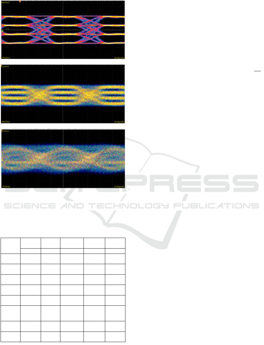
From the signal quality analyzer, a 50 Gb/s (25
Gbaud) PAM-4 electrical eye diagram was measured,
as shown in Figure 15(a), and the eye diagram was
with a rise time of 8.0 ps, a fall time of 8.3 ps, a
peak-to-peak time jitter of 16.1 ps, an SNR of 4.02,
and a total amplitude of 300.4 mV. From the
voltage-to-current converter, Figure 15(b) shows the
50 Gb/s PAM-4 eye diagram with a rise time of 21.4
ps, a fall time of 18.0 ps, a peak-to-peak time jitter
of 40.1 ps, an SNR of 1.77, and an amplitude of 38.9
mV. From the output of the TIA chip on PCB,
Figure 15(c) shows the 50 Gb/s PAM-4 eye diagram,
but the signal quality was bad and the parameters of
the eye diagram could not be obtained. Because the
quality of the current signal from the voltage-to-
current converter was not good, the output signal
quality of the TIA could not become better. The
amplitude between two levels of a PAM-4 signal is
smaller, so the amplitude of the PAM-4 signal needs
to be amplified as possible as large. If the TIA chip
can be tested with a PD, the output signal of the TIA
can have better quality.
According to the post simulations of the TIA, the
performance of our TIA circuit and the comparison
with other literatures are summarized in Table 1.
The figure of merit (FOM) is defined as (2) and (3).
Our TIA had a high FOM value because the TIA had
low power consumption and small chip area.
However,
the transimpedance gain and output
amplitude of our TIA chip still need to be improved
for PAM-4 applications.
FOM1
Gain
dBΩ
BandwidthGHz
Power
m
W
ChipAreamm
2
(2)
FOM2
Gain
dBΩ
BitrateGb/s
Power
m
W
ChipArea
mm
2
(3)
(a)
(b)
(c)
Figure 13: Measured 25 Gb/s NRZ eye diagrams form (a)
the pattern generator, (b) the voltage-to-current converter,
and (c) the TIA chip on a PCB.
Figure 14: Measured 32 Gb/s NRZ eye diagram from the
TIA chip on a PCB.
25 Gb/s NRZ and 50 Gb/s PAM-4 Transimpedance Amplifier with Active Feedback and Equalization in 90 nm CMOS Technology
255
(a)
(b)
(c)
Figure 15: Measured 50 Gb/s PAM-4 eye diagrams form
(a) the pattern generator, (b) the voltage-to-current
converter, and (c) the TIA chip on a PCB.
Table 1: Comparison of the performance of the TIA
circuits.
Ref.
Kim
2014
Liao
2007
Han
2010
Hiratsuka
2018
This work
Post-Sim. Measure Post-Sim. Measure Post-Sim.
CMOS
Tech.
65 nm 90 nm 130 nm 65 nm 90 nm
Gain
(dBΩ)
52 66 60 52.3 34
BW
(GHz)
50 29 12.6 12.6 26
Bit rate
(Gb/s)
52 40 20 25 50
Power
(mW)
49.2 75 38.3 3.96 11.6
Area
(mm
2
)
0.48 0.15 0.22
0.63
(0.0064
Core Area)
0.15
FOM1 110.1 170.1 89.7
264.1
(26001)
508.0
FOM2 114.5 234.7 142.4
524.1
(51590)
977.0
4 CONCLUSIONS
We propose a wide-bandwidth and high-linearity full
differential TIA circuit in CMOS 90nm technology.
The TIA used the active feedback to replace the
feedback resistor and to reduce the chip area. The
equalizer was also used in the TIA to compensate for
the high-frequency response of the TIA and to
extend the bandwidth. The transimpedance gain,
bandwidth, and input referred current noise density
were about 34 dBΩ, 26 GHz, and 74 pA/
√
Hz
,
respectively. The power consumption of the TIA
chip was about 11.6 mW, and the chip area was
0.343 × 0.440 mm
2
. Below the peak-to-peak input of
1.1 mA, the TIA can have good linearity. The 25
Gb/s NRZ and 50 Gb/s PAM-4 eye diagrams of the
TIA were simulated, and the 25 Gb/s NRZ, 32 Gb/s
NRZ and 50 Gb/s PAM-4 eye diagrams of the TIA
were measured. In 25 Gb/s NRZ and 50 Gb/s PAM-
4 simulations, the TIA circuit had good
performance. Because the input current signal was
degraded by the voltage-to-current converter, the
TIA output signal cannot obtain clear eye diagram
for 50 Gb/s PAM-4 measurements. Our TIA chip
could be used in 25 Gb/s NRZ and 50 Gb/s PAM-4
optical receivers for 200 Gb/s and 400 Gb/s high-
speed optical transmissions.
ACKNOWLEDGEMENTS
This paper is supported by the Taiwan
Semiconductor Research Institute and the Taiwan
Ministry of Science and Technology (MOST 107-
2218-E-992-304 and MOST 107-2637-E-992-011).
REFERENCES
Baveja, P. P., Li, M., Chen, Y., et al, 2018. Demonstration
of 53.125 Gb/s, CWDM, PAM-4, directly modulated
laser transmission over 20 km SMF. In Optical Fiber
Communication Conference, M1E.3.
Bhoja, Sudeep, 2017. PAM4 signaling for intra–data
center and data center to data center connectivity
(DCI). In Optical Fiber Communication Conference,
W4D.5.
Han, J., Choi, B., Seo, M., et al., 2010. A 20-Gb/s
transformer-based current-mode optical receiver in
0.13-μm CMOS. IEEE Transactions on Circuits and
Systems II: Express Briefs, 57(5), pp. 348-352.
Hiratsuka, A., Tsuchiya, A., Tanaka, K., et al, 2018. A low
input referred noise and low crosstalk noise 25 Gb/s
transimpedance amplifier with inductor-less
OPTICS 2019 - 10th International Conference on Optical Communication Systems
256

bandwidth compensation. 2018 IEEE Asian Solid-
State Circuits Conference, pp. 69-72.
Kim, S. G., Jung, S. H., Eo, Y. S., et al., 2014, A 50-Gb/s
differential transimpedance amplifier in 65nm CMOS
technology. In 2014 IEEE Asian Solid-State Circuits
Conference (A-SSCC), pp. 357-360.
Lakshmikumar, K., Kurylak, A., Nagaraju, M., et al, 2018.
A process and temperature insensitive CMOS linear
TIA for 100 Gbps/λ PAM-4 optical links. In 2018
IEEE Custom Integrated Circuits Conference.
Liao, C. F., Liu, S. I., 2007. A 40Gb/s transimpedance-
AGC amplifier with 19dB DR in 90nm CMOS.
In 2007 IEEE International Solid-State Circuits
Conference. Digest of Technical Papers, pp. 54-586.
Salhi, S., Escid, H., & Slimane, A, 2017. Design of high
speed transimpedance amplifier for optical
communication systems. 2017 Seminar on Detection
Systems Architectures and Technologies.
Seng, C. W., Sern, T. Y., Seng, Y. K., 2013. A low power
wideband differential transimpedance amplifier for
optical receivers in 0.18-μm CMOS. In 2013 IEEE
11th international new circuits and systems
conference (NEWCAS), pp. 1-4.
Szczerba, K., Westbergh, P., Karout, J., et al., 2012. 4-
PAM for high-speed short-range optical
communications. IEEE/OSA Journal of Optical
Communications and Networking, 4(11), pp. 885-894.
Talluri, G. R., Rakesh, K. K., & Baghini, M. S., 2015. A
4–14 Gbps inductor-less adaptive linear equalizer
using hybrid filter in 65 nm CMOS technology.
In Sixteenth International Symposium on Quality
Electronic Design, pp. 90-97.
Xie, Y., Li, D., Liu, Y., et al, 2018. Low-noise high-
linearity 56Gb/s PAM-4 optical receiver in 45nm SOI
CMOS. 2018 IEEE International Symposium on
Circuits and Systems.
25 Gb/s NRZ and 50 Gb/s PAM-4 Transimpedance Amplifier with Active Feedback and Equalization in 90 nm CMOS Technology
257
