
Buck Converter Modeling in High Frequency using Several Transfer
Function-based Approaches
Imen Shiri, Sanda Lefteriu and C
´
ecile Labarre
Unit
´
e de Recherche en Informatique et Automatique, IMT Lille Douai, 941, rue Charles Bourseul, 59500 Douai, France
Keywords:
Buck Converter, Modeling, Transfer Function, High Frequency, Parasitic Elements.
Abstract:
The recent development of large gap (GaN) components adapted to high frequency operation opens
up interesting perspectives for the emergence of high power density static converters. However, the
implementation of GaN components requires the development of new characterization, modeling and design
methods adapted to these fast components. In this paper, we present three modeling techniques for a static
converter in the frequency domain. They are all characterizing the input - output transfer function and they
are: the average model, the generalized transfer function (GTF) and the modified nodal analysis technique
(MNA). These models, already existing in the literature, are extended to account for the parasitic effects of the
switching elements (diodes or transistors). In fact, parasitic elements associated with the different passive and
active components are inherent in a power electronics structure. Their effects are negligible in low frequency
but they are preponderant in high frequency. Simulation results performed for a Buck converter show that,
while the GTF and the MNA are able to predict the resonances present at multiples of the switching frequency,
the average model does not. In terms of the influence of the parasitic elements on the transfer function, the
peak which is due to the output filter parameters is attenuated. Lastly, the experimental validation shows that,
even with the introduction of the parasitic elements of the switching components, there are still discrepancies
between the models and the data, so additional parasitics still need to be accounted for.
1 INTRODUCTION
Static converters allow the electric power source
(a battery, the electrical network, a solar panel,
etc.) to be adapted to the needs of the receiver
(an electric motor, an asynchronous machine, etc.).
In the literature, time domain models, based on
the analysis of the converter’s dynamics described
by differential equations, have been proposed :
state space averaging (SSA) (Biolkova et al., 2010)
(Behjati et al., 2013) (Anun et al., 2013), the hybrid
model (Benmansour, 2009) to name a few. Frequency
domain models have also been proposed, such as the
average model, the GTF (Biolek et al., 2006) and
the MNA (Trinchero, 2015). With the improvement
of switching component’s performance (IGBT, diode)
such as the speed, these models describing the
frequency behavior should be developped further.
Our objective is to describe the behavior of a
converter in the frequency domain using the transfer
function.
Power converters contain diodes and transistors,
hence they fall under the category of switching
systems. These switches move between an ON state
and an OFF state periodically. Thus, neglecting
non-idealities, power converters can be considered
as linear periodic systems varying in time. For this
reason, the concept of the transfer function needs to
be redefined and adapted.
To start with, we are interested in the Buck DC-
DC converter, which can be used for the control of
DC motors, to regulate the speed of rotation of a DC
motor in both directions of rotation, battery chargers,
solar chargers, etc.
The average model describes the dynamics of
the system as a function of the average values for
the current and voltage variables, thus neglecting the
effects due to switching. The Generalized Transfer
Function (Biolek, 1997) is based on the small signal
analysis technique to obtain the transfer function. It
combines the continuous behavior (due to storage
elements) and discrete behavior (due to switches)
with a single transfer function. Since DC-DC
converters are considered as periodic switched linear
systems (PSL), they can be characterized by a time-
variant transfer function, which takes into account
722
Shiri, I., Lefteriu, S. and Labarre, C.
Buck Converter Modeling in High Frequency using Several Transfer Function-based Approaches.
DOI: 10.5220/0007927407220729
In Proceedings of the 16th International Conference on Informatics in Control, Automation and Robotics (ICINCO 2019), pages 722-729
ISBN: 978-989-758-380-3
Copyright
c
2019 by SCITEPRESS – Science and Technology Publications, Lda. All rights reserved

the time-varying behavior, or alternatively, by the bi-
frequency transfer function. For such circuits, their
steady-state response may be found as the solution of
a MNA equation (Trinchero, 2015).
This paper is a follow-up to the publication
(Lefteriu and Labarre, 2016). It compares
the three transfer function modeling techniques
for computing the magnitude of the frequency
response of a Buck converter, this time integrating
the parasitic elements of the diode and the
transistor. Ideally, switching should be between
0 and the final value instantaneously. To obtain
an improved frequency model, wide-bandwidth
components have to be considered: equivalent
series resistance, lumped shunt parasitic capacitance
(Davoudi, 2010). Adding these components
complicates models already proposed. As a first
contribution of our paper, the average model was
rederived using the descriptor system (Verghese et al.,
1981). As a second contribution, the GTF (Biolek
et al., 2006) and the MNA (Trinchero, 2015) were
adapted to the new setting.
This paper is structured as follows. In Sect. 2,
we describe the effects of parasitics on the switching
signals. In Sect. 3, the Buck converter with
parasitic elements is described in terms of the average
model. In Sect. 4, the modeling technique using
the generalized transfer function is re-derived. The
extension of the technique proposed in (Trinchero,
2015) is presented in Sect. 5. Sect. 6 presents
simulation results and, finally, the conclusion and
directions for future research are given in Sect. 7.
2 EFFECTS OF PARASITIC
ELEMENTS ON THE
SWITCHING SIGNALS
The Buck converter is a hybrid dynamical system
with the continuous behavior dictated by the linear
time-invariant elements (resistor, capacitor, inductor)
and the discrete behavior given by the switches
(transistor, diode). Fig. 1 shows the topology of a
Buck converter which supplies a passive load resistor
with the voltage V
out
.
The IGBT is represented by the switch S and the
diode by the switche S. The switch S is controlled by a
pulse width modulation signal (PWM), a binary input
signal. When S = 1, the switch is closed (conducting),
and for S = 0 the switch is open (non-conducting).
Fig. 2 shows the case of ideal switching and the
voltage measured across the IGBT. The plot for V
ds
in
Fig. 2b shows an exponentially decaying sinusoidal
−
+
V
in
S
PWM
S
L
C
R
V
out
Figure 1: Topology of the Buck converter.
(a) Ideal swiching (b) IGBT switching
Figure 2: Voltage in case of ideal switching and across the
IGBT.
signal which can be explained by the presence of a
second-order circuit given by parasitic RLC elements.
As in any semiconductor component, there is
a parasitic capacitance in the IGBT and diode
that models the inverse polarized P-N junction and
disrupts the operation in high frequency. This
capacitance will be set in parallel. To obtain the
ripples, the IGBT and the diode will be modeled,
in addition to the ideal switches, by an equivalent
series resistance, and an equivalent series inductance.
Fig. 3 shows the proposed model taking into account
parasitics for an IGBT and a diode.
r
1
L
1
S
C
1
(a) IGBT
r
2
L
2
S
C
2
(b) Diode
Figure 3: Equivalent models.
Integrating the proposed models into the Buck
converter, Fig. 4 shows the topology of the Buck
converter from Fig. 1 with parasitic elements. We
have also accounted for the line inductance L
s
.
3 AVERAGE MODEL
In continuous current mode (CCM), the current in the
inductor never reachs zero and the Buck converter is
described by two circuit typologies, namely:
• S = 1, S = 0 in the time interval t ∈ [kT, (k +α)T]
Buck Converter Modeling in High Frequency using Several Transfer Function-based Approaches
723

−
+
V
in
r
1
L
1
i
L
1
S L
s
i
L
s
L
i
L
C
R
S
L
2
i
L
2
r
2
C
2
C
1
V
out
Figure 4: Topology of the Buck converter with parasitic elements.
• S = 0, S = 1 for t ∈ [(k + α)T, (k + 1)T ],
with T , the switching period and k = 0, 1, 2, . . .. The
duty cycle α indicates the percentage of time that the
switch S is ON during the switching period. In each
of these operation modes, the behavior is linear, hence
the circuit can be modeled by differential equations
involving the inductors’ currents i
Ls
i
L1
, i
L2
, i
L
and
the voltages over the capacitors V
c1
,V
c2
, V
c
. The
introduction of parasitic inductances in series with
the switches results in the current variables through
the switches being 0 during one of the two operating
modes. Eventually, this yields to state equations
with different state variables depending on the mode,
hence a descriptor-form representation of the circuit is
more appropriate. A descriptor system is of the form
(Verghese et al., 1981):
E
˙
x(t) = Ax(t) + BV
in
(t)
V
out
(t) = Cx(t) + DV
in
(t),
(1)
with the matrix E non-invertible. In our case, the state
vector contains the variables i
Ls
i
L1
, i
L2
, i
L
, V
c1
,V
c2
,
V
c
, hence it has dimension 7. This yields E and A of
dimension 7 × 7, while B and C
T
are of dimension
7 × 1. Lastly, D is scalar.
In the first mode, i
L2
= 0, hence
E
1
i, j
=
0, i 6= j & i = j = 3
1, i = j 6= 3
(2)
A
1
=
0 0 0 0 −
1
L
s
−
1
L
s
0
0 −
r
1
L
1
0 0
1
L
1
0 0
0 0 1 0 0 0 0
0 0 0 0 0
1
L
−
1
L
1
C
1
−
1
C
1
0 0 0 0 0
1
C
2
0 0 −
1
C
2
0 0 0
0 0 0
1
C
0 0 −
1
RC
(3)
B =
1
L
s
0 0 0 0 0 0
T
(4)
C =
0 0 0 0 0 0 1
(5)
D = 0. (6)
Similarly, in the second mode, i
L1
= 0, hence
E
2
i, j
=
0, i 6= j & i = j = 2
1, i = j 6= 2
(7)
A
2
=
0 0 0 0 −
1
L
s
−
1
L
s
0
0 1 0 0 0 0 0
0 0 −
r
2
L
2
0 0
1
L
2
0
0 0 0 0 0
1
L
−
1
L
1
C
1
0 0 0 0 0 0
1
C
2
0 −
1
C
2
−
1
C
2
0 0 0
0 0 0
1
C
0 0 −
1
RC
(8)
and B, C, D are the same as in Eq. (4)-(6).
The average model neglects the switching effects
and considers the average value of the state variables
over the switching period. This amounts to
considering the average of the descriptor matrices in
the two operating modes:
E = αE
1
+ (1 − α)E
2
(9)
A = αA
1
+ (1 − α)A
2
. (10)
The average of the B, C, D in the two modes yields the
same expressions as in Eq. (4)-(6). This results in an
equation of the form (1) and the transfer function can
be easily obtained by applying the Laplace transform:
H
avg
(s) =
V
out
(s)
V
in
(s)
= C(sE − A)
−1
B + D. (11)
4 GENERALIZED TRANSFER
FUNCTION (GTF)
The development of the Generalized Transfer
Function relies on the solution to the state-space
differential equation
˙
x(t) = Ax(t) + BV
in
(t). (12)
The solution for the state x(t) depends on the initial
condition x
0
at time t
0
and the input V
in
(t) (Antoulas,
ICINCO 2019 - 16th International Conference on Informatics in Control, Automation and Robotics
724

2005):
x(t) = e
A(t−t
0
)
x(t
0
) +
Z
t
t
0
e
Aτ
BV
in
(t − τ)dτ, t ≥ t
0
.
(13)
The reason why a standard-state space formulation
is considered here, instead of the descriptor-form, is
because the solution equivalent to (13) would be more
difficult to derive. However, the descriptor realization
with the singular E is not needed, as long as special
care is taken to account for the zero state variables
present in each mode.
In mode 1, the state variable i
L2
= 0, hence the
circuit can be modeled by differential equations of
the form (12) involving the remaining non-zero state-
variables. The resulting state-space matrix A
1
is
obtained by deleting the 3
rd
row and column of the
matrix in (3). Naturally, the B and C are the same
as in (4)-(5), but without the 3
rd
entry. Evaluating the
solution (13) at the end of phase 1 (t ∈ [kT, k T + αT ]),
we obtain:
x
1
(kT+αT)=e
A
1
αT
x
1
(kT)
+
Z
kT +αT
kT
e
A
1
τ
B
1
V
in
(kT+αT−τ)dτ.
(14)
Accounting for i
L2
= 0, we obtain the state vector x(t)
by premultiplying x
1
(t) with the matrix P
1
∈ R
7×6
:
x(t) = P
1
x
1
(t), where P
1
=
1 0 0 0 0 0
0 1 0 0 0 0
0 0 0 0 0 0
0 0 1 0 0 0
0 0 0 1 0 0
0 0 0 0 1 0
0 0 0 0 0 1
.
In mode 2, the state variable i
L1
= 0 and the circuit
can be modeled by differential equations of the form
(12) involving the remaining non-zero state-variables.
The resulting state-space matrix A
2
is obtained by
deleting the 2
nd
row and column of the matrix in (8).
Naturally, B and C are the same as in (4)-(5), but
without the 2
nd
entry. Evaluating the solution (13) at
the end of phase 2 (t ∈ [kT + αT, kT + T ]), we obtain:
x
2
(kT + T ) =e
A
2
(1−α)T
x
2
(kT + αT )
+
Z
kT +T
kT +αT
e
A
2
τ
B
2
V
in
(kT + T − τ)dτ.
(15)
Accounting for i
L1
= 0, we obtain the state vector x(t)
by premultiplying x
2
(t) with the matrix P
2
∈ R
7×6
:
x(t) = P
2
x
2
(t), where P
2
=
1 0 0 0 0 0
0 0 0 0 0 0
0 1 0 0 0 0
0 0 1 0 0 0
0 0 0 1 0 0
0 0 0 0 1 0
0 0 0 0 0 1
.
We replace (14) into (15):
x(kT + T ) = e
A
2
(1−α)T
0
e
A
1
αT
0
x(kT ) (16)
+ e
A
2
(1−α)T
0
Z
kT +αT
kT
e
A
1
τ
0
P
1
B
1
V
in
(kT+αT−τ)dτ
+
Z
kT +T
kT +αT
e
A
2
τ
0
P
2
B
2
V
in
(kT + T − τ)dτ,
where e
A
2
0
is a notation for P
2
e
A
2
P
T
2
and e
A
1
0
is a
notation for P
1
e
A
1
P
T
1
. Naturally, P
T
1
P
1
= I and
P
T
2
P
2
= I, where I is the identity matrix. Hence,
P
T
1
B
1
= P
T
2
B
2
= B, with B given in (4).
Applying the small signal analysis, the input
is taken as a constant voltage together with a
small amplitude AC component V
in
(t) = V
0
+
˜
V
in
e
jΩt
,
V
0
>>
˜
V
in
with Ω, the perturbation frequency of
choice. The steady-state output voltage will be
composed of a DC component and several AC
components. By analogy with linear-time invariant
systems, only the component with frequency Ω is of
interest, the other frequencies which appear due to the
non-linearity of the overall system being disregarded.
The generalized transfer function for the line-to-
output response is given by evaluating H
GT F
(s) on the
imaginary axis at s = jΩ for various values of Ω:
H
GT F
(s)=C
I−G
2
G
1
z
−1
−1
G
2
ˆ
H
1
(s)z
−(1−α)
+
ˆ
H
2
(s)
where z = e
sT
and
G
1
= e
A
1
αT
0
G
2
= e
A
2
(1−α)T
0
H
1
(s) =
Z
αT
0
e
A
1
τ
0
Be
−sτ
dτ
H
2
(s) =
Z
T
αT
e
A
2
τ
0
Be
−sτ
dτ.
5 AUGMENTED MNA FOR PSL
CIRCUITS
This section applies the approach initially proposed
in (Trinchero, 2015) for the computation of the
steady-state of periodic switched linear circuits, to
the computation of the small-signal transfer function
Buck Converter Modeling in High Frequency using Several Transfer Function-based Approaches
725

−
+
V
in
g
1
jωL
1
(2) (4) (3) (1) (5) (8)
(6)
(7)
Y
S
1
jωL
s
jωL
jωC
G
Y
S
2
jωL
2
g
2
jωC
2
jωC
1
Figure 5: Frequency domain representation of the Buck converter with parasitic elements.
of Buck converters which accounts for parasitic
elements. The bi-frequency transfer function is:
H(ω, Ω) =
Z
∞
−∞
Z
∞
−∞
h(t, τ)e
− j(ωt−Ωτ)
dtdτ (17)
and the output in the frequency domain is :
Y (ω) =
1
2π
Z
∞
−∞
H(ω, Ω)U (Ω)dΩ, (18)
where U is the input, Ω and ω are the input and output
frequencies. This shows that a sinusoidal input with
frequency Ω produces an output with a rich spectrum,
as opposed to LTI systems, for which the output
contains solely the frequency Ω. The time-varying
transfer function H(t, Ω) =
R
∞
−∞
h(t, τ)e
− jΩ(t−τ)
dτ, is
related to the bi-frequency transfer function as
H(ω, Ω) =
Z
∞
−∞
H(t, Ω)e
j(Ω−ω)t
dt. (19)
For periodically switched linear circuits, H(t, Ω) is
a periodic function of t which can be written as a
Fourier series with respect to the switching frequency
ω
s
=
2π
T
:
H(t, Ω) =
n=∞
∑
n=−∞
H
n
(Ω)e
jnω
s
t
, (20)
with the frequency-dependent Fourier coefficients
H
n
(Ω) called aliasing transfer functions:
H
n
(Ω) =
1
T
Z
T
0
H(t, Ω)e
− jnω
s
t
dt.
The output in the frequency domain is obtained by
substituting (19) and (20) into (18):
Y (ω) =
n=∞
∑
n=−∞
H
n
(ω − nω
s
)U(ω − nω
s
). (21)
The frequency domain representation of a Buck
converter is obtained by substituting the switch S and
S in Fig. 4 with the periodic switching admittance
element respectively Y
S1
and Y
S2
. Fig. 5 shows
the frequency domain representation of the buck
converter with parasitcis elements. Compared to
the model proposed by (Trinchero, 2015), the MNA
equation will be modified to account for the presence
of L
i
, r
i
, C
i
, i=1,2, yielding:
M(ω) H
H
T
N(ω)
V(ω)
I(ω)
=
G(ω)
F(ω)
, (22)
where:
V(ω) = (V
1
V
2
V
3
V
4
V
5
V
6
V
7
V
8
)
T
(23)
I(ω) = (I
L
s
I
L
1
I
L
2
I
L
)
T
(24)
G(ω) =
0 0 0 0 0 0 0 0
T
(25)
F(ω) =
−V
in
0 0 0
T
(26)
H
T
=
I −I 0 0 −I 0 0 0
0 0 −I I 0 0 0 0
0 0 0 0 0 I −I 0
0 0 0 0 I 0 0 −I
(27)
N(ω) =
− jω
ω
ωL
S
0 0 0
0 − jω
ω
ωL
1
0 0
0 0 − jω
ω
ωL
2
0
0 0 0 − jω
ω
ωL
(28)
M(ω) =
a −h −c
1
0 0 0 0 0
−h b
1
0 −d
1
0 0 0 0
−c
1
0 c
1
0 0 0 0 0
0 −d
1
0 d
1
0 0 0 0
0 0 0 0 b
2
−d
2
0 0
0 0 0 0 −d
2
d
2
0 0
0 0 0 0 0 0 c
2
0
0 0 0 0 0 0 0 f
(29)
where a = jω
ω
ωC
1
+ Y
s
1
,
h = jω
ω
ωC
1
,
ICINCO 2019 - 16th International Conference on Informatics in Control, Automation and Robotics
726

b
i
= jω
ω
ωC
i
+ g
i
, where g
i
=
1
r
i
, i = 1, 2,
c
i
= Y
s
i
, i = 1, 2,
d
i
= g
i
I, i = 1, 2,
f = jω
ω
ωC + G, where G =
1
R
.
Each block in (22) is of dimension 2N +1. Ideally,
N should be large because we are computing an
infinite sum as shown in (21). In particular, the matrix
ω
ω
ω is equal to
ω
ω
ω=diag
ω
0
−Nω
s
. . . ω
0
−ω
s
ω
0
ω
0
+ω
s
. . . ω
0
+Nω
s
where ω
0
is the excitation frequency. Moreover, Y
s
1
and Y
s
2
are matrices of the form
Y
s
i
=
Y
i,0
Y
i,−1
. . . Y
i,−2N
Y
i,1
Y
i,0
. . . Y
i,−2N+1
.
.
.
.
.
.
.
.
.
.
.
.
Y
i,2N
Y
i,2N−1
. . . Y
i,0
, i = 1, 2
(30)
where Y
1,n
are the Fourier coefficients of the window
function with amplitude 1 and period T
s
when the
switch S is on:
Y
1,n
=f
s
Z
αT
0
e
− jnω
s
t
dt=
e
− jnω
s
αT
−1
− j2πn
, n=−2N, . . . , 2N,
and Y
2,n
are the Fourier coefficients of the same
window function delayed by αT for S: Y
2,n
=
Y
1n
e
− jω
s
nαT
, n=−2N, . . . , 2N.
Last, but not least, the unknowns in (23)-(24)
contain the coefficients of the truncated frequency
domain representation with 2N + 1 terms. For
example, for I
L
, this would be I
L
(ω) =
∑
N
n=−N
I
n
δ(ω−
nω
s
− ω
0
).
Small-signal analysis assumes an input obtained
from the superposition of a constant and a small-
amplitude AC component V
in
(t) = V
0
+
˜
V
in
e
jΩt
, with
V
0
>>
˜
V
in
and Ω, the perturbation frequency of
choice. This corresponds to a sum of 2 Dirac
distributions in the frequency domain:
V
in
(ω) = V
0
δ(ω) +
˜
V
in
δ(ω − Ω).
Hence, the linear system in (22) should be solved for
each value of the excitation frequency ω
0
= 0 and
ω
0
= Ω. The output voltage is the voltage at node
8 in Fig. 5 and is expressed as V
8
= V
8,DC
+ V
8,AC
,
where
V
8,DC
(ω) =
N
∑
n=−N
V
n,DC
δ(ω − nω
s
), (31)
V
8,AC
(ω) =
N
∑
n=−N
V
n,AC
δ(ω − nω
s
− Ω), (32)
with the coefficients V
n,DC
and V
n,AC
found by solving
the linear system in (22) for ω
0
= 0 and ω
0
= Ω,
respectively. The transfer function at perturbation
frequency Ω is
H
MNA
( jΩ) =
(
V
0,AC
˜u
, if Ω 6= nω
s
V
n,DC
+V
0,AC
˜u
, if Ω = nω
s
. (33)
When the perturbation frequency Ω is an integer
multiple of the switching frequency ω
s
, there are
components due to the DC input which also contribute
to the response.
6 RESULTS
Simulation results comparing the three modeling
techniques detailed in the previous sections, namely
the average model, the Generalized Transfer Function
and the augmented MNA, are applied to a Buck
converter with and without parasitics. The parameters
for the Buck converter are L = 1mH, C = 500µF,
R = 12Ω. For simplicity, we considered that the IGBT
and the diode have the same values for the parasitic
elements: L
1
= L
2
= 100nH, C
1
= C
2
= 1.4nF and
r
1
= r
2
= 0.2Ω. The line inductance is taken as L
s
=
500nH. The switching frequency is f
s
= 20kHz=
1
T
and the duty cycle is α =
1
2
.
For comparison, the magnitude of the Bode plot
was measured with an Agilent spectrum analyzer
operating between 9kHz and 3GHz. For low
frequencies, measurements were performed with an
oscilloscope.
Fig. 6 shows the frequency response obtained
with the average model in the ideal case and when
including parasitics. The two average models do not
predict the peaks due to switching. The amplitude
of the low frequency resonance (due to the converter
output filter) is slightly smaller when including
parasitic elements. Moreover, the average model
with parasitics detects a high frequency resonance at
around f = 15MHz. These observations are explained
by the poles of the two models shown in Table 1. The
ideal case corresponds to a second-order system with
only two poles, while the parasitics add 5 more poles.
Table 1: Poles of the two average models: with and without
parasitic elements.
With without
−1.8 · 10
2
± 1.4 · 10
3
i −8.3 · 10
1
± 1.4 · 10
3
i
−6.1 · 10
5
0
−5 · 10
5
± 4.2 · 10
7
i 0
−1.9 · 10
5
± 6.8 · 10
7
i 0
From these values, we notice that the peak in low
frequency is explained by the fact that the imaginary
Buck Converter Modeling in High Frequency using Several Transfer Function-based Approaches
727
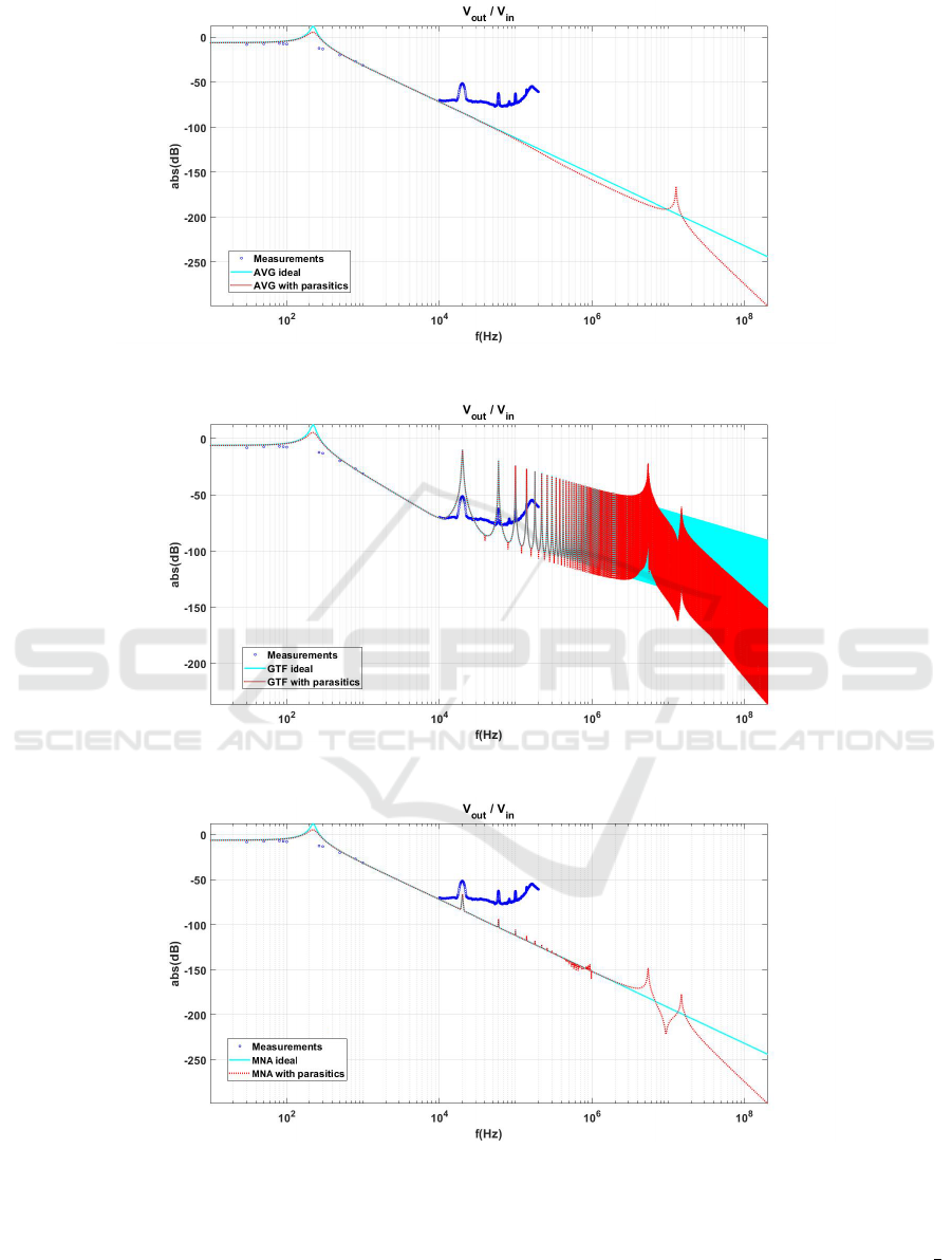
Figure 6: Simulation result: Average model.
Figure 7: Simulation result: GTF.
Figure 8: Simulation result: MNA.
part is almost identical and the real part decreases. In
addition to that, two other pairs of complex conjugate
poles appear at around f = 15MHz.
Fig. 7 shows the response computed with the
generalized transfer function for the ideal case, as
well as the case with parasitics. This approach
predicts the peaks at odd multiples of the switching
frequency (due to choosing the duty cycle as α =
1
2
,
the even multiples are not present). The amplitude
of these peaks computed with GTF is higher than
ICINCO 2019 - 16th International Conference on Informatics in Control, Automation and Robotics
728

those measured. In addition to these peaks, the GTF
predicts two resonances at around 5.42MHz and 15
MHz for the case with parasitics.
Last, but not least, the response computed with
the MNA approach is shown in Fig. 8. The MNA
is also able to predict the peaks in the frequency
response at odd multiples of the switching frequency,
however, these peaks are decreasing in amplitude.
The amplitude of these peaks is lower than those
shown by the measurements. In addition to these
peaks, the MNA predicts, as the GTF two resonances
at around 5.43MHz and 14 MHz for the case with
parasitics.
7 CONCLUSION AND FUTURE
WORK
The transfer function for a Buck power converter
with parasitic elements taken into consideration for
the switching devices was computed with three
approaches: the average model, the GTF and
the MNA for PSL circuits. These approaches
were compared against each other and against
the measurements. Our analysis shows that the
introduction of parasitic elements has an effect on
the low frequency resonance, this resonance being
due to the converter’s output filter. Moreover,
the GTF and MNA predict two additional peaks
resonances at arround 5MHz and 14 MHz due to
the parasitic’s elements. At odd multiples of the
switching frequency, we noticed a negligible effect
of the parasitics. In the future, we will improve
our model in the following ways. First, we will
determine the correct values of the parasitic elements
from the switching signal. Second, we will also take
into consideration the parasitic elements of the output
filter’s inductance, capacitance and resistance.
ACKNOWLEDGEMENTS
This work has been achieved within the framework
of the CE2I project (Convertisseur d’Energie Integre
Intelligent). CE2I is co-financed by European Union
with the financial support of European Regional
Development Fund (ERDF), the French State and the
French Region of Hauts-de-France.
REFERENCES
Antoulas, A. C. (2005). Approximation of large-scale
dynamical systems, volume 6. SIAM.
Anun, M., Ordonez, M., and Luchino, F. (2013). Topology
zero: A generalized averaging equivalent circuit
model for basic DC-DC converters. In 2013 IEEE
14th Workshop on Control and Modeling for Power
Electronics (COMPEL), pages 1–7.
Behjati, H., Niu, L., Davoudi, A., and Chapman, P. L.
(2013). Alternative time-invariant multi-frequency
modeling of PWM DC-DC converters. IEEE
Transactions on Circuits and Systems I: Regular
Papers, 60(11):3069–3079.
Benmansour, K. (2009). R
´
ealisation d’un banc d’essai pour
la Commande et l’Observation des Convertisseurs
Multicellulaires S
´
erie: Approche Hybride. PhD thesis,
Cergy-Pontoise.
Biolek, D. (1997). Modeling of periodically switched
networks by mixed S-Z description. IEEE
Transactions on Circuits and Systems I: Fundamental
Theory and Applications, 44(8):750–758.
Biolek, D., Biolkov
´
a, V., and Dobes, J. (2006). Modeling
of switched DC-DC converters by mixed S-Z
description. In 2006 IEEE International Symposium
on Circuits and Systems, pages 4–pp.
Biolkova, V., Kolka, Z., and Biolek, D. (2010). State-space
averaging (SSA) revisited: on the accuracy of SSA-
based line-to-output frequency responses of switched
DC-DC converters. 2:1.
Davoudi, A. (2010). Reduced-order modeling of power
electronics components and systems. PhD thesis,
University of Illinois at Urbana-Champaign.
Lefteriu, S. and Labarre, C. (2016). Transfer function
modeling for the buck converter. In 2016 IEEE 20th
Workshop on Signal and Power Integrity (SPI), pages
1–4.
Trinchero, R. (2015). EMI Analysis and Modeling of
Switching Circuits. PhD thesis, Politecnico di Torino.
Verghese, G., L
´
evy, B., and Kailath, T. (1981). A
generalized state-space for singular systems. IEEE
Transactions on Automatic Control, 26(4):811–831.
Buck Converter Modeling in High Frequency using Several Transfer Function-based Approaches
729
