
RFID Tag Antennas Designed by Fractal Features and
Manufactured by Printing Technology
Chi-Fang Huang
1
, Jing-Qing Zhan
1
and Tsung-Yu Hao
2
1
Graduate Institute of Communication Engineering
Tatung University, Taiwan
2
Dept. of Graphic Communications and Publishing
Shih Hsin University, Taiwan
Abstract. Based on the fractal features, this work is to design RFID Tag anten-
nas with minimum area needed as a tag. The designed passive tag is to be re-
sponsible for the EM wave of 915MHz from the reader. The concept of com-
plex conjugated matching is used in designing the antenna. Electromagnetic
Simulation tool is also used to help this design as well. The techniques of
measuring the material parameters necessary in the design procedure are also
mentioned in this paper. Offset printing technology is employed to manufac-
ture these tag antennas which is assumed as a kind of low-cost tags. Real per-
formance of these tags is also shown in this work.
1 Introduction
Even invented and applied initially during the World War II, RFID (Radio Frequency
Identifi-cation) [1] has attracted much attention recently. Precisely speaking, RFID
has been applied very widely in some proprietary or closed systems, for example,
animal control, portal control (access badges), etc. in last decades. The main advan-
tages of RFID application are, storing item data in an electronic way, data access by
electromagnetic wave, and allowing multiple accesses to RFID tags. Based on the
diverse applications, different spectrum bands are allocated, for example, LF (125 -
134.2 kHz and 140 - 148.5 kHz) for animal control, HF (13.56MHz) for electronic
ticket, and UHF (868 MHz-928 MHz) for logistics, etc. Most of the frequencies are
located in the ISM (Industrial, Scientific and Medical) bands [1].
However, RFID was emphasized again mainly because of the need of supply chain
[2]. By proposing a standard for the format of electronic data used for goods items,
of which EPC (Electronic Product Code) [3] is an example, the products can be regis-
tered at once when they are shipped out from the factories, and be released when they
are checked out at the counter of a supermarket. This is called “product tracking” and
is to be carried out in an “Internet of Thing”.
When the RFID tags are used in the logistics, they are not supposed to be recycled
after being used. Therefore, the cost of tag will be a key factor to determine if this
technology can be widely applied or not. There are three parts composing the tag
Huang C., Zhan J. and Hao T. (2007).
RFID Tag Antennas Designed by Fractal Features and Manufactured by Printing Technology.
In Proceedings of the 1st International Workshop on RFID Technology - Concepts, Applications, Challenges, pages 93-99
DOI: 10.5220/0002418400930099
Copyright
c
SciTePress
cost, namely, antenna, chip and assembly for them. It has been believed that, apply-
ing the traditional printing technologies [4] to produce the antennas will lower the
cost of the antenna part. One of the major efforts of this present work is to produce
the tag antenna by traditional offset printing method to demonstrate the possibilities
of making low-cost tags in high-volume.
Based on the fractal features [5], this work is to design RFID Tag antenna with
minimum area used as a tag. Usually the fractal antennas own the characteristic fea-
tures of minimization, wideband and multi-band. As a matter of fact, design by frac-
tals is also able to give an engineering path to follow in the simulation procedure
when searching for the target. As a RFID application in UHF band [6], the designed
passive tag is to be responsible for the EM wave of 915MHz from the reader.
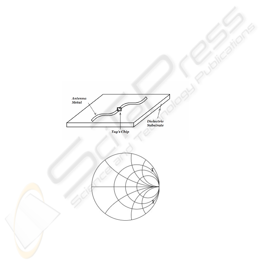
Referring to Figure 1, RFID tag antenna is a kind of planar antenna, in which the
antenna metal layer is laminated on a dielectric substrate. Usually, even they look
diverse in shape in RFID Tag industry; the type of dipole antenna is used for the tags
operating at frequency for UHF band and for higher bands. In designing such a kind
of tag, the material parameters, for example, the conductivity
σ
of the antenna metal
and the dielectric constant
r
ε
, are necessary to be given in the simulation phase. In
this work, the measurement techniques of material parameters are also mentioned.
Performance evaluation both by simulation and measurement are shown in this paper.
Fig. 1. The physical structure of a RFID tag.
Fig. 2. Situation of complex conjugated impedance matching on the Smith Chart.
94
2 Design of Tag Antenna Using Fractal Features
The operation in a tag is that, the antenna receives the incoming EM energy and trans-
fers into the chip; and chip sends back the data-modulated EM wave to the RFID
reader. As depicted in Figure 1, to ensure the efficiency of energy transfer in between
chip and antenna, they should be in a “match” condition. In ordinary antenna indus-
try, the antenna is designed with a standard input impedance, for instance,
Ω50
or
Ω75
, to have impedance match with transceivers or other RF devices. However, in
the RFID Tag industry, for the purpose of cost-down, usually the match network
inside the chip is not offered. Consequently, it needs a complex conjugated matching
to ensure highest power transfer in between the chip and antenna, namely, to maxi-
mize the tag performance. Those two “X” marks show the input impedance positions
of the chip and antenna on the Smith Chart in Figure 2. Most of the cases, chip’s is
the lower “X”, and antenna’s is the other one. That means, usually the chip is capaci-
tive; and the antenna for being designed should be inductive. The present tag antenna
is developed based on this theory.
As an EM design tool, CST [7] is employed to help design antenna prototype.
Since there two kinds of material are involved in the tag, and since this tag antenna is
to be printed on paper by offset printing technology, before beginning the design, the
conductivity
σ
of the conductive ink, the paper’s dielectric constant
r
ε
and its asso-
ciated loss tangent
δ
tan
should be given. The lithographic conductive ink used in
this work is CLO-101A purchased from Precisia LLC [8], and its corresponding con-
ductivity
σ
was measured based on the technique described in the literature [9][10].
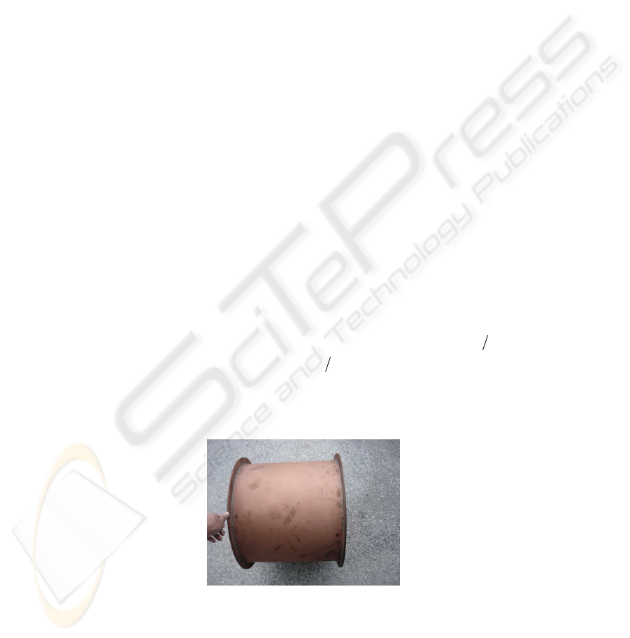
The metal cylindrical cavity shown in the Figure 3 is used to measure the ink’s con-
ductivity according to that theory. The ink is coated on the inner side of the right and
left planar walls of this cavity. The measured conductivity is
mS
6
1085.3 ×
, which
is only 6.6% or so of the copper’s
mS
7
108.5 ×
. As what expected, such a kind of
ink is not as good as ordinary conductors to be antenna radiating material. This
should be seriously taken into account when the tag performance is emphasized and
they are produced by printing technologies.
Fig. 3. Metal cylindrical cavity for measuring the ink’s conductivity.
95

Fig. 4. Rectangular cavity for measuring the dielectric constant of coated paper.
On the other hand, the dielectric constant
r
ε
of the coated paper, which is used as
the substrate of the tag, can be obtained by applying the technique of cavity resonator
[11][12]. By this method, referring to Figure 4, the frequency response is measured
two times at least for this rectangular cavity with different height. The paper layers
are contained in this cavity in measurement. The resultant dielectric constant
r
ε
of
paper used is 2.83 and its
δ
tan
is 0.046 around the frequency 915MHz. This shows
that the paper is of a little loss and should be carefully considered.
To have a path to follow for designing the antenna shape that is of complex conju-
gate matching with the chip, the fractal is used to generate it. Among the fractal ge-
ometries, the Sierpinski gasket fractal is adopted to develop, see Figure 5.
The chip used in this project is the XRA00 of Alien Technology [13], which has
an input impedance
Ω
− 4.1977.6 j
. Hence, the target impedance for the antenna is
Ω
+ 4.1977.6 j
in theory. Fig. 6 is the simulation model established in the CST
package for a tag antenna. It is based on the Sierpinski gasket fractals. In addition to
generating fractals through different stages, the rectangular dimension of this tag is
also under adjustment to search for the target input impedance of the antenna. Table
1 shows the simulated input impedance of this fractal antenna due to different dimen-
sion. Some of the candidates in this table are to be printed and analyzed later.
Fig. 5. Sierpinski gasket fractals.
Fig. 6. Simulation model of a tag antenna in the EM package CST
96
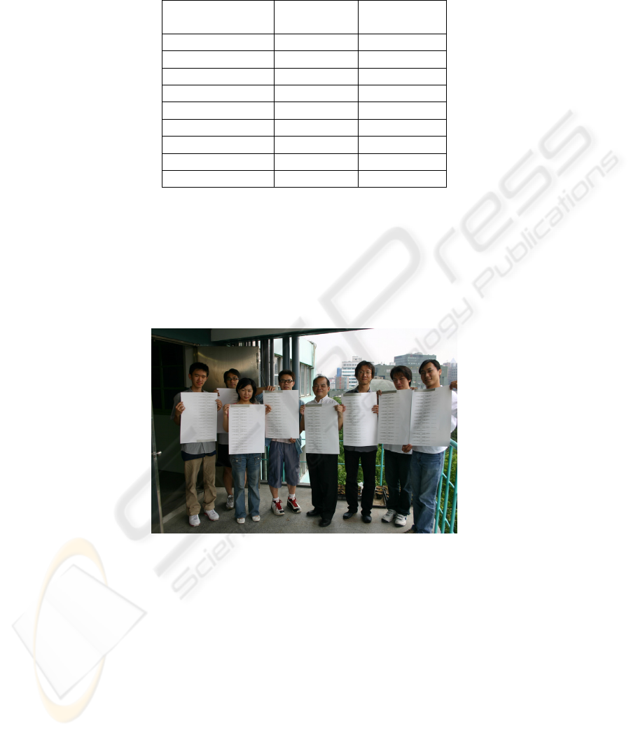
Table 1. Simulated input impedance of the tag antenna.
Tag dimension
mm x mm
R (
Ω
) jX (
Ω
)
10 x 120 9.211 31.86j
10 x 130 9.614 51.86j
10 x 140 10.32 75.71j
10 x 150 10.08 91.83j
10 x 160 9.728 119.4j
10 x 170 12.95 145.6j
10 x 180 15.04 178.5j
10 x 190 18.31 221.8j
10 x 200 20.15 281.3j
3 Printing Tag Antenna and Performance Analysis
Figure 7 shows a demonstration of the printed paper sheets on which many tag anten-
nas had been printed by offset printing technology. This antenna is based on the
simulation results mentioned above and operating in UHF band.
Fig. 7. Demonstration of high-speed production of RFID tag by offset printing technology.
Figure 8 shows the details of this printed tag antenna with a dimension 10mm x
180mm. In an antenna anechoic chamber, by using a UHF reader in measurement,
this tag’s responsible distance is about 1m. For the purpose of comparison, around
the same dimension, this antenna shape have also been made by screen printing and
by ordinary PCB process, the former can reach to 1.5 m and the latter can reach up to
3.4m. These antennas are supposed not perfectly matched with the chip. The farther
distance they can make is because the screen printing can print thicker film than off-
set printing does; and the PCB process is to provide 0.018mm thick metal layer of
copper. Less conductive ink, thinner printed ink’s layer and substrate with higher
97

loss (coated paper) indeed make the tag antennas produced by offset printing technol-
ogy less efficiency. Anyway, its unique advantage is to able produce tags in high-
speed and in high volume, yet being low-cost.
Fig. 8. A single RFID tag of UHF band made by offset printing technology.
4 Conclusion
This paper has outlined and demonstrated a complete procedure by which the offset
printing technology is applied to produce high volume and low-cost RFID tags.
Based on the concept of complex conjugated matching, the design for tag antenna is
carried out firstly by the help of the EM simulation package. To precisely design the
antenna by computer simulation, the techniques of measuring material parameters
given in literatures are also applied to obtain those parameters of conductive ink and
paper. By the up-to-date offset printing machine, the tag antenna had been printed
out by a high-speed manner to demonstrate its possibility to be a low-cost product.
Acknowledgements
This project was granted by Tatung Company [14], Taipei, TAIWAN, who plays the
main role offering long-term support for the academic-industrial projects being car-
ried on in Tatung University. Sun Sui Print Co., Ltd, Taipei County, TAIWAN, is
appreciated for their kind support to provide the offset machines in printing the RFID
tags designed in the present work. Moreover, we want to specially thank Mr. Wen-
Ho Wu, the factory manager of this company. Without his professional guide in the
printing procedure, this present work would not be done completely.
References
1. Finkenzeller, Klaus: RFID Handbook: Fundamentals and Applications in Contactless
Smart Cards and Identification, Wiley & Sons Ltd. New York, 2
nd
edition. (2003)
2. Bansal, R., “Coming soon to a Wal-Mart near you,” IEEE Antennas Propag. Mag., vol. 45,
pp. 105–106 (2003)
98

3. Sarma, S., Brock, D. and Engels, D., “Radio frequency identification and the electronic
product code,” IEEE Micro, pp. 50-54. (2001)
4. Blayo, Anne and Pineaux, Bernard, “Printing Processes and their Potential for RFID Print-
ing,” Joint sOc-EUSAI conference. (2005)
5. Werner, Douglas H. and Ganguly, Suman, “An Overview of Fractal Antenna Engineering
Research,” IEEE Antennas and Propagation Magazine, Vol. 45, No. 1, pp. 38-57. (2003)
6. Rao, K. V. S., Nikitin, P. V. and Lam, S. F., “Antenna Design for UHF RFID Tags: A
Review and a Practical Application,” IEEE Trans. Antennas and Propagation, Vol. 53, No.
12, pp. 3870-3876. (2005)
7. http://www.cst.com
8. http://www.precisia.net
9. Otoshi, Tom Y. and Franco, Manuel M., “The Electrical Conductivities of Steel and Other
Candidate Materials for Shrouds in a Beam-Waveguide Antenna System,” IEEE Transac-
tions on Instrumentation and Measurement, Vol. 45, No. 1, pp. 77-83. (1996)
10. Clauss, R. and Potter, P. D., “Improved RF Calibration Techniques – A Practical Tech-
nique for Accurate Determination of Microwave Surface Resistivity,” JPL Technical Re-
port 32-1526, Vol. XII, pp. 59-67.
11. Huang, Chi-Fang, “A Cascaded 2-D Array of Microstrip Antenna,” Tatung Journal, Vol.
XIV, pp. 69-83. (1984)
12. Richards, W. F., Lo, Y. T. and Brewer, J., “A simple experimental method for separating
loss parameters of a microstrip antenna,” IEEE Trans. Antennas Propagat., vol. AP-29, pp.
150-151. (1981)
13. http://www.alientechnology.com
14. http://www.tatung.com
99
