A MICRO ULTRA LOW POWER RF RADIO FOR NEURAL
SIGNAL RECORDING
Rui Zhong, Richard Liu
Cullen College of Engineering,University of Houston, 4800 Calhoun Road, Houston, Texas, United States
Haleh Fotowat, Fabrizio Gabbiani
Department of Neuroscience, Balor College of Medicine, Houston,Tx, United States
Keywords: Micro Radio, Neural Signal Recording, RF Radio, Ultra Low Power.
Abstract: This paper reports the development of a small, light-weight and mini-battery operated low power radio
transmitter for neural signal recording. This system allows recording of neural signal down to the level of 50
μV. A micromachined electrode is used to obtain these signals. The neural signal is then amplified 10,000
times and transmitted to the receiver at 433 MHz. The manufactured radio system is 7 mm by 6 mm in size
and 0.5 gram in weight, with a power consumption of 750 μW. Radio functionality is tested and verified on
locusts.
1 INTRODUCTION
Wireless recording of neural activity from the
central and peripheral nervous systems has long
been pursued by physiologists as a way to
understand the operation of individual neurons, to
decipher the relationship between the environment
stimuli, nerve system response and the activities
generated by the nerve signal (Akin, 1998). One of
such research area is visually guided escape
behaviors, which are critical to the survival of many
animals.
In this design, we are required to detect the
neural signals from main nerves of a locust.
Therefore a small size, light weight and low power,
cell battery based RF wireless telemetry system is
needed. Unfortunately, the power consumption of
available commercial radio chips is too large to be
sustained by a small cell battery. In this design, we
simplified the radio structure as much as possible to
reduce power consumption. Firstly, a RF BJT
oscillator is used to generate the carrier, instead of a
Frequency Synthesizer. Secondly, AM modulation
scheme is used instead of the typical FSK
modulation in commercial radio chips. Thirdly, the
whole system is analog. At last, a 30 AWG copper
wire with the length of 40mm is used as antenna
with the radio transmitter working at 420 MHz.
After several experiments, it is verified that this
design is small enough to be carried by a locust and
light enough to allow the bug to jump as usual. The
received signal provides strength and time
information of the neural activities.
2 RADIO SYSTEM DESIGN
2.1 System Overview
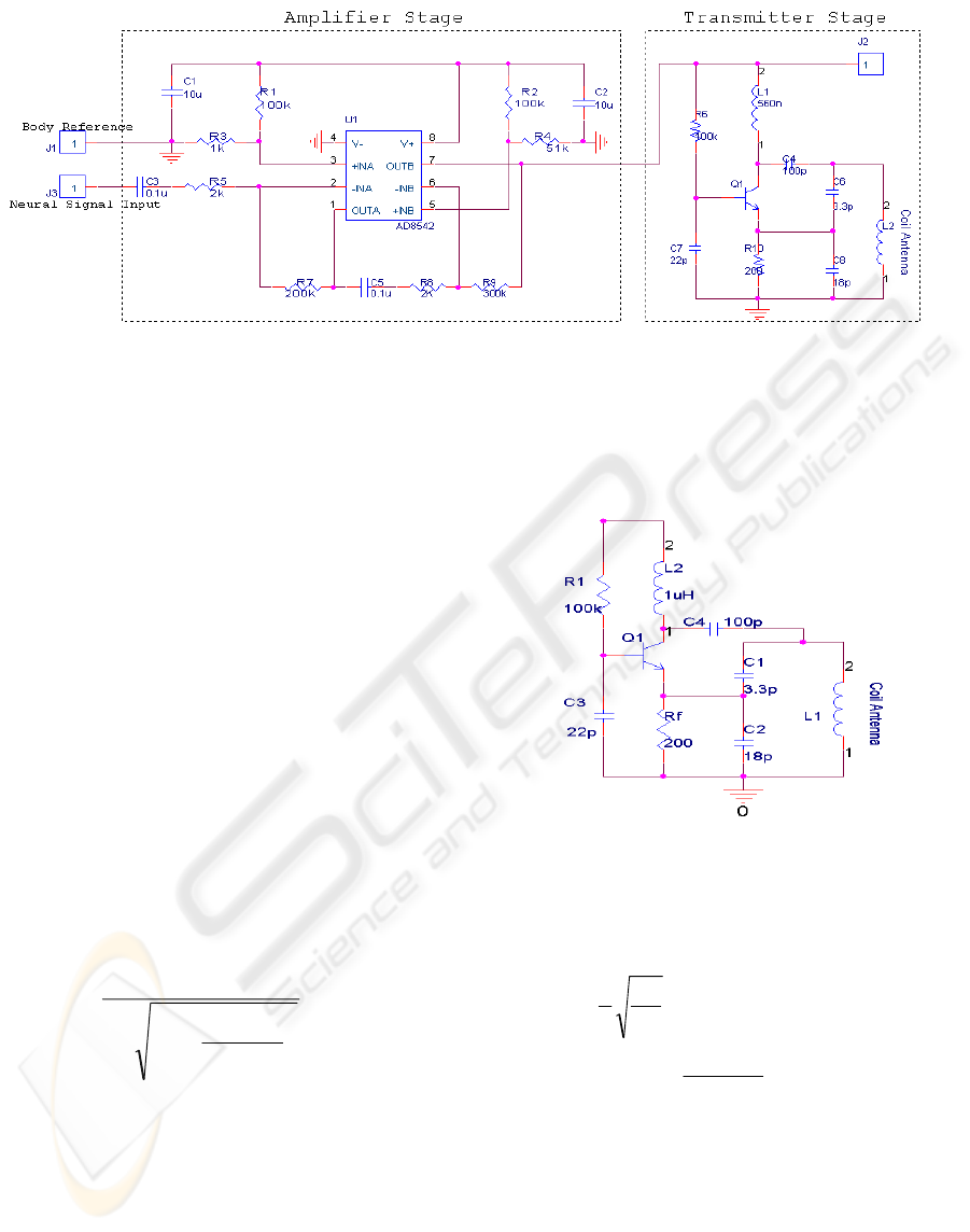
The radio transmitter is divided into two functional
parts: amplifier stage and transmitter stage. Detected
neural signals are typically in the range of 50 to 150
micro volts. In order to process this signal, a high
gain amplifier stage is used to amplify it 10,000
times. The amplified neural spikes are then sent to
the transmitter stage for transmitting. Direct
coupling is used between these two stages. The
whole system runs on a 3 Volts cell battery and the
power consumption is only 750 μW in total. The
complete system schematic is shown in Figure 1
236
Zhong R., Liu R., Fotowat H. and Gabbiani F. (2008).
A MICRO ULTRA LOW POWER RF RADIO FOR NEURAL SIGNAL RECORDING.
In Proceedings of the First International Conference on Biomedical Electronics and Devices, pages 236-239
DOI: 10.5220/0001055702360239
Copyright
c
SciTePress

Figure 1: System Overview.
2.2 Transmitter Stage
For most neural experiments, researchers are mainly
interested in the when this signal is generated and
how many neural spikes are observed, other than
their accurate amplitude value. Thus, simplifying the
transmitter design has little influence on the research
itself, but it can greatly reduce the power
consumption, and reduce the size and weight of the
system.
In our design, the transmitter is basically a 433
MHz BJT Colpitts oscillator. Colpitts Oscillator is
well known for its simplicity and robustness. Figure
2 is the structure of our transmitter stage, which is a
common-base (CB) Colpitts oscillator. In Figure 2
we can see that C1, C2 and L1 forms the positive
feed back loop, and R1, L2 and R
F
provide the DC
bias for oscillation. C3 is the capacitor for common
base structure.
Because of its wide application area, Colpitts
oscillator is well studied. The oscillation frequency
of this circuit can be calculated by equation (1).
⎟
⎟
⎠
⎞
⎜
⎜
⎝
⎛
+
⋅
⋅
=
21
21
1
0
2
1
CC
CC
L
f
π
(1)
In this Colpitts oscillator application, the
operation frequency is about 433 MHz. Therefore,
several issues need to be taken care of. These issues
will be discussed in the following subsections.
2.2.1 Selection of Inductor L1
Three issues are important when deciding the L1
inductor value.
First, according to equation (1), the value of L1
is directly related to the oscillation frequency. For
433 MHz band operation, it is usually in the nano-
Henry range.
Figure 2: Transmitter Structure.
Second, the value of inductor L1 is also related
to the quality factor of Oscillation. The relation is
expressed in Equation (2).
∑
∝
C
L
r
Q
1
1
(2)
Where
21
21
CC
CC
C
+
⋅
=
∑
(3)
And
r
is the serial resistance of L1.
In the oscillation loop, larger quality factor Q
leads to more stable and accurate oscillation and
lower power dissipation. From equation (2), for the
same
∑
C , greater L1 and smaller
r
will contribute
to a higher system quality factor. This indicates that
we should choose a high Q inductor, whose
r
is
A MICRO ULTRA LOW POWER RF RADIO FOR NEURAL SIGNAL RECORDING
237

small. And the L1 to
∑
C ratio should be large
enough.
Finally, up limit does exist for the value of L1.
Increase L1 too much will decrease its self-resonant
frequency and force the corresponding
∑
C decrease
to the BJT’s parasitic capacitance region, which may
cause unstable oscillation (Razavi, 1998).
The selection of L1 value is a compromise
between these issues discussed above.
2.2.2 Selection of C1 and C2
According to the analysis in section 2.2.2, to achieve
a higher quality factor, C1 and C2 should be as small
as possible. On the other hand, however, C1 and C2
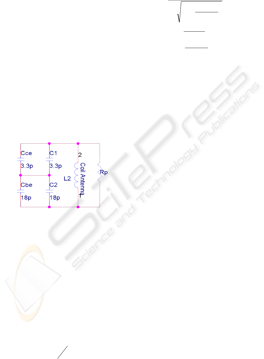
can not be too small. Because C1 is in parallel with
the junction capacitance C
CE
and C2 is in parallel
with the junction capacitance C
BE
, Rp is the
equivalent resistance. Its relation to the loop is
shown in equation (4). The equivalent oscillation
loop is shown in Figure 3.
Figure 3: Equivalent Oscillation Loop.
Figure 3 tells us if C1 and C2 are too small, Cce
and Cbe will dominate the oscillation frequency.
Typically, C1 and C2 should be greater than Cce and
Cbe. Therefore,
∑
C should lies inn the range of 1 pf
to 4 pf.
Also, known
∑
C , the value of C1 to C2 directly
depends on their ratio, C1/C2. Again, compromise
exists when selecting this ratio. Smaller C1/C2 ratio
means larger loop quality factor but smaller positive
feedback gain, while larger C1/C2 ratio gives greater
feedback gain but lower quality factor (Razavi,
1998). In practice, experiment shows that 3.3pf and
18pf capacitor pair gives stable oscillation and
makes it easy to start the oscillation. Now, we can
modify equation (1) to obtain practical equation for
oscillation frequency f
0
.
m
P
g
CC
R
2
21
)/1( +
=
(4)
⎟
⎟
⎠
⎞
⎜
⎜
⎝
⎛
+
⋅
⋅
=
21
21
1
0
''
''
2
1
CC
CC
L
f
π
(5)
Where
CE
CE
CC
CC
C
+
⋅
=
1
1
1
'
(6)
And
BE
BE
CC
CC
C
+
⋅
=
2
2
2
'
(7)
2.2.3 Selection of Rf and R1
R
F
is a DC negative feedback resistor, which helps
stabilize the transistor current gain. R1 is used to set
up the collector I
C
. However, R
F
and R1 are also the
main power consumption components in this circuit.
The power they consume can be estimated by
equation (7) and (8).
fCRf
RIP ∗=
2
(7)
1
2
1
RIP
BR
∗= (8)
Since I
C
is usually large, R
F
should be as small as
possible. And because I
B
is typical in uA range, thus
P
R1
is usual less than 50 uW. In practical design, for
the purpose of low power consumption, we
simultaneously decrease R
F
and increase R1, the
final power consumption of the oscillation is only
750 uW, compared to the typical 10 mW power
consumption for a commercial transmitter, this is a
great advantage.
2.3 Amplifier Stage
Figure 6 is the structure for amplifier stage. It
consists of two JFET operational amplifiers. Each
stage runs on a single power supply and has a gain
of 100. To save power, an OPA with only 40 uA
current consumption at 2V is used. Important design
rules about amplifier stage are exploded below.
2.3.1 Power Line Decoupling
In practical application, the battery has non-zero
internal impedance, which induces AC voltage on
the power line.
If not carefully decoupled, the AC voltage on the
power becomes an input to amplifier stage. This will
cause the amplifier stage self-oscillate. Also, smaller
R20 and R19 (as shown in Fig 4) value may be
necessary to further ensure no self-oscillation will
occur.
BIODEVICES 2008 - International Conference on Biomedical Electronics and Devices
238

Figure 4: Amplifier Stage Structure.
2.3.2 Direct Coupling
In this design, we can use the DC bias component of
the OPA as the power supply voltage V
CC
for the
next transmitter stage. Therefore, a direct coupling is
used between amplifier stage and transmitter stage.
When no neural signal input appears, the output
voltage of the amplifier should be half of the battery
voltage. That is the V
CC
power supply for the next
transmitter stage.
When neural signal is connected to the amplifier
input, the amplified signal of interest will directly
couples to transmitter, that is add to V
CC
3 EXPERIMENT RESULTS
Figure 5 shows the radio installed on a locust. A pair
of micromachined electrode is used to collect neural
signal from the locust. Figure 6 demonstrates the
neural spikes collected and observed at the receiver
side oscilloscope.
Figure 5: Locust with micro radio installed.
Figure 6: a) neural spikes measured on the transmitter
side b) neural spikes observed on the receiver
oscilloscope.
4 CONCLUSIONS
This paper discusses a design scheme of a single
BJT transistor oscillator based RF Radio for neural
signal recording. Comparing to other radio existing,
this design has two important advantages. First, it is
an ultra low power radio, with a power consumption
of only 750 uW, only 7.5% of the available
commercial transceiver chips. This feature makes it
possible to be powered by a tiny watch battery.
Second, this radio is small and light, it is only 7 mm
by 6 mm in size and 0.5 gram in weight. These two
advantages make this radio especially suitable for
wireless recording tasks performed on small
animals, insect, such as locusts and pigeons. The
communication range of this radio is up to 20 feet.
REFERENCES
Akin, T., 1998. A Wireless Implantable Multichannel
Digital Neural Recording System for a
Micromachined Sieve Electrode, Solid-State Circuit,
VOL 33, No 1. IEEE Journal of.
Razavi, B., 1998. RF Microelectronics, Prentice-Hall, Inc.,
New York, 2nd edition.
A MICRO ULTRA LOW POWER RF RADIO FOR NEURAL SIGNAL RECORDING
239
