
A LOW-POWER INTEGRATED CIRCUIT FOR ANALOG SPIKE
DETECTION AND SORTING IN NEURAL PROSTHESIS SYSTEMS
A. Bonfanti
†§
, T. Borghi
§
, R. Gusmeroli
§
, G. Zambra
§
, A. S. Spinelli
§
, A. Oliynyk
∗
L. Fadiga
†∗
and G. Baranauskas
†
†
Department of Robotics, Brain and Cognitive Sciences, The Italian Institute of Technology - Genova, Italy
§
Dipartimento di Elettronica e Informazione, Politecnico di Milano - IU.NET, Milano, Italy
∗
Dipartimento di Scienze Biomediche e Terapie Avanzate, Sezione di Fisiologia umana, Universit´a di Ferrara - Ferrara, Italy
Keywords:
Prosthetic device, Action potential (AP), Multichannel recording system, Spike detection, Spike sorting.
Abstract:
Since the proof that prosthetic devices directly controlled by neurons are viable, there is a huge increase in
the interest in integrated multichannel recording systems that register neural signals with implanted chronic
electrodes. One of the bottlenecks in such compact systems is the limited rate of data transmission in the wire-
less link, requiring some sort of data compression/reduction. To solve such a problem, we propose an analog
low power integrated system for action potential (AP) detection and sorting. In this system, AP detection is
performed by a double threshold method that reduces the probability of false detections while AP sorting is
based on the measurement of peak and trough amplitudes and spike width. The circuit has been implemented
in 0.35−µm CMOS technology with power consumption of 70 µW per channel including the pre-amplifier.
The system was tested with real traces. Compared to standard AP sorting techniques, the proposed simple AP
sorter was able to correctly assign to single units over 90% of detected APs. Thus, our system preserves most
information encoded by APs and we estimate that for a typical trace the required bandwidth per channel will
be less than 4 kbps or 400 kbps for 100 channel.
1 INTRODUCTION
In recent years, in a number of laboratories it has
been shown that signals obtained with multichan-
nel extracellular recordings are sufficient to con-
trol the movements of a prosthetic device in real
time (Hochberg et al., 2006). However, we are still
far away from any device to be clinically tested be-
cause of enormous technological and scientific chal-
lenges (Stieglitz, 2007). According to current think-
ing, a future neural prosthetic device should con-
tain a set of neural amplifiers connected to a signal-
processing unit and a wireless link to transmit the
amplified signals down to an actuator (e.g., a robotic
arm, a remote controller, a mouse, and so on). Unfor-
tunately, the low power state-of-the-art wireless sys-
tems cannot transmit data at the high rate required for
this kind of application where power budget is lim-
ited to 800 µW/mm
2
(Harrison and Charles, 2003).
For example, 100 channels sampled at 30 kHz with
10 bits resolution would require to transmit 30 Mbps
while low power wireless systems can handle only
< 3 Mbps (Olsson et al., 2005). Thus, to enable
data transmissions from multichannel neural ampli-
fiers, it is necessary to compress or reduce raw neural
data. Since in a typical neural trace only action po-
tentials (APs) contain any useful information, a very
efficient way of neural signal reduction is to trans-
mit a single bit for each AP. Researchers in (Harri-
son et al., 2007) used simple threshold detectors to
identify APs in the amplifier signal and then trans-
mitted zeros when no AP were detected and ones
for each threshold crossing event. However, each
recording site usually collects the activity from sev-
eral nearby neurons and the aforementioned method
does not provide information on which neuron fired
at a given time. This may be a serious drawback in
motor prostheses applications where it is important
to isolate the activity of each neuron to better predict
the intended movement (Hochberg et al., 2006). This
paper presents a low-power circuit that permits neu-
ron discrimination while drastically reducing the re-
quired data bandwidth per channel. This circuit ex-
tracts three parameters for a single spike, namely the
67
Bonfanti A., Borghi T., Gusmeroli R., Zambra G., S. Spinelli A., Oliynyk A., Fadiga L. and Baranauskas G. (2009).
A LOW-POWER INTEGRATED CIRCUIT FOR ANALOG SPIKE DETECTION AND SORTING IN NEURAL PROSTHESIS SYSTEMS.
In Proceedings of the International Conference on Biomedical Electronics and Devices, pages 67-74
DOI: 10.5220/0001539200670074
Copyright
c
SciTePress
peak and trough amplitudes and the time between the
peak and the trough. It has been shown that the use
of these AP features is sufficient to adequately sorts
APs and is actually superior to spike spike separa-
tion using more parameters (Vibert and Costa, 1979).
According to (Olsson et al., 2005), for sampling rate
of 20 kHz at 5 bit resolution, a similar AP feature
extraction method yields data compression close to
90%. Although a similar in function analog device
has been described (Horiuchi et al., 2004) a digital ex-
traction of these three parameters has been presented
also (Olsson et al., 2005), in this work we introduce
significant innovations: a) the implementation of a
new spike-detection algorithm that decreases several-
fold the rate of false detections; b) an improved peak
and trough detectors with very fast recovery time per-
mitting the detection of closely spaced APs, and c)
the use of an additional feature, namely the time dif-
ference between peak and trough occurrence. More-
over, the amplification of neural signals is performed
with an amplification topology that provides the best
known trade-off between noise and power consump-
tion. To confirm the efficiency of our device, we
tested it employing artificial and real signals and we
conclude that, in the majority of cases, with few in-
dependent units present in a trace, the extracted three
parameters can be sufficient to achieve adequate sin-
gle unit separation.
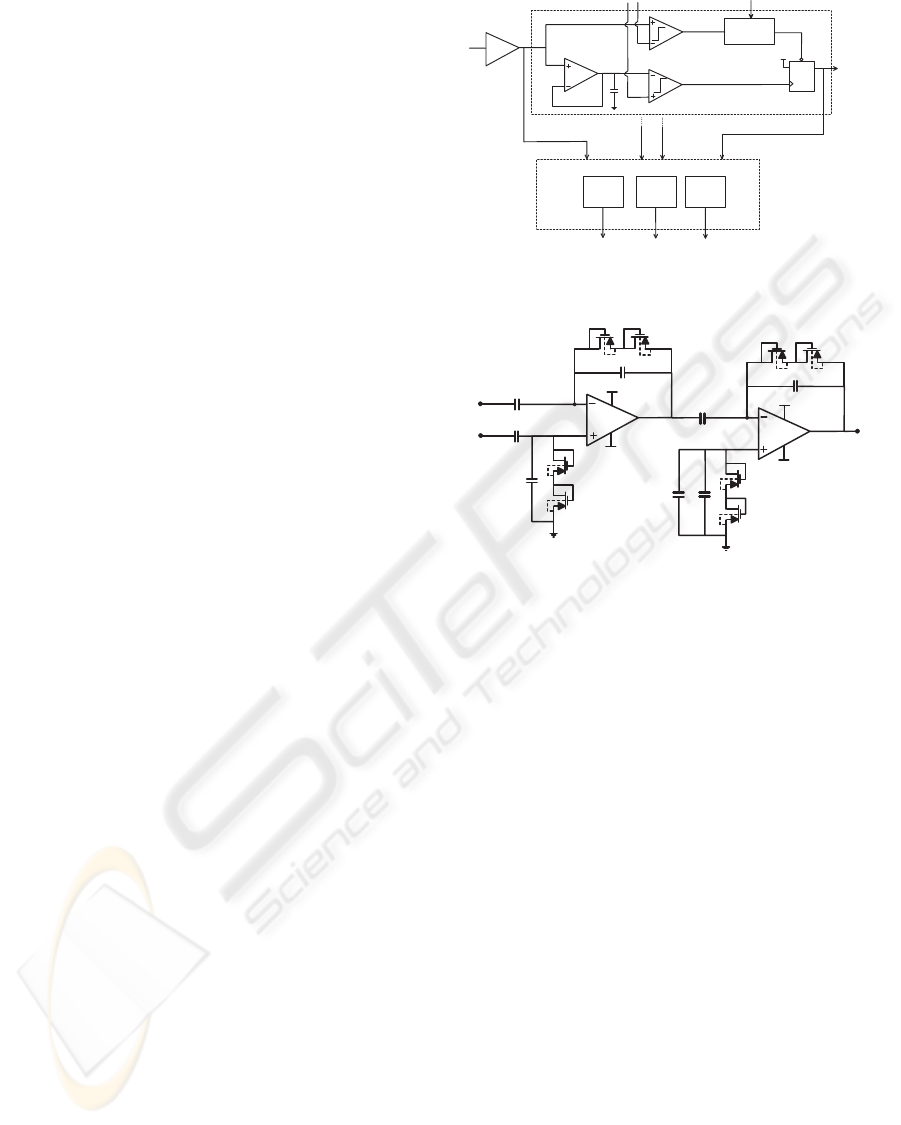
2 SYSTEM ARCHITECTURE
The system architecture is shown in Fig. 1 and com-
prises a low-noise amplifier (LNA), a spike detec-
tor and a spike sorter. The spike detector splits the
amplified signal in two paths and exploits a double-
threshold strategy, which will be discussed in detail
in Section 2.2. The signal coming from the LNA
is also processed by the spike sorter, which extracts
from each detected spike three features, namely the
peak and trough amplitudes and the time interval be-
tween peak and trough. The detailed circuit and its
performance descriptions follows below.
2.1 Low-power and Low-noise Neural
Amplifier
Pre-amplification is obtained through a double-stage
active filter, shown in Fig. 2. The first stage is
an ac-coupled inverting high-pass filter, employing
two MOS-bipolar pseudoresistors as feedback ele-
ments (Harrison and Charles, 2003). This enables
the synthesis of high-value resistance without large
area consumption. Mid-band gain is set to G
1
=
V
H
C
G
M
L N A
W I N D O W
G E N E R A T O R
C K
R N
F F
D
Q
S P I K E D E T
P E A K
D E T E C T O R
T R O U G H
D E T E C T O R
T R O U G H
P E A K
W I D T H
D E T E C T O R
V
I N
P O S S P I K E
N E G S P I K E
V
D D
T I M E W I N D O W
V
L
W I N D O W
C O N T R O L
S P I K E
D E T E C T O R
S P I K E
S O R T E R
W I D T H
T I M E W I N D O W
P O S S P I K E
Figure 1: Block scheme of the detection and sorting system.
+ V
D D
- V
D D
C
1
T E L E
O P A M P
V
I N
V
R E F
+ V
D D
2 S T A G E S
O P A M P
- V
D D
C
1
C
2
C
3
C
4
C
3
C
4
C
2
V
O U T
Figure 2: Overall schematic of the pre-amplifier (LNA).
−C
1
/C
2
= −66, with C
1
= 10 pF and C
2
= 150 fF.
The higher cut-off frequency is determined by the
gain-bandwidth product of the first operational am-
plifier (GBWP
1
) and is set to about GBWP
1
/G
1
=
20 kHz, while the high-pass pole frequency was de-
signed to be about 10 Hz as determined by C2 and
MOS pseudoresistors . The second stage was de-
signed to reject the first stage offset while provid-
ing further signal amplification and filtering. This
stage employs the same pseudoresistor elements in
the feedback path, with a gain G
2
= −50 (achieved
with C
3
= 7.5 pF and C
4
= 150 fF). The operational
amplifier in the first stage was designed to have an
input-referred noise in the pre-amplifier band lower
than 5 µV
rms
. Furthermore, since this circuit is
thought to be used in an implantable system with a
large number of electrodes, the current consumption
was minimized by designing a telescopic operational
amplifier (see Fig. 3); in fact, this well-known con-
figuration gives excellent noise performance thanks
to the limited number of transistors and can achieve
the best trade-off between power consumption and
noise. The input PMOS and current mirror NMOS
transistors are biased in weak-inversion and strong in-
version region (Harrison and Charles, 2003), respec-
tively, since (W/L)
p
≫ (W/L)
n
(see Table 1, where
IC is the inversion coefficient which is << 1 in the
BIODEVICES 2009 - International Conference on Biomedical Electronics and Devices
68
weak-inversion region). This implies that M
P
transis-
tors have a transconductance much higher than M
N
ones and hence the equivalent input-referred noise is
mainly determined by the the input transistors of the
differential pair. Considering both the flicker noise
and the thermal noise, the input referred power noise
density results:
E
2
n
eq
=
8KTγ
g
mp
+
2K
(1/ f)
p
C
′
ox
W
p
L
p
1
f
, (1)
with γ equal to 1/(2κ) in weak-inversion region (κ ≈
0.7). In this working region the transconductancemay
be approximated by:
g
m
∼
=
κI
D
U
T
, (2)
and so the input-referred thermal noise spectral den-
sity results:
E
2
n
th
=
8kTU
T
κ
2
I
bias
, (3)
where I
bias
is the total current consumption of the tele-
scopic cascode amplifier. Setting an upper limit for
the thermal noise contribution in the 20-kHz ampli-
fier band of 3 µV
rms
, a bias current of 4 µA has to be
chosen. The flicker noise contribution was carefully
minimized choosing a large area for the input PMOS
transistors, W
p
×L
p
= 400 × 1 µm
2
, that implies a
noise corner frequency lower than 100 Hz assuming a
flicker noise coefficient K
(1/ f)
p
≈ 2 ×10
−26
V
2
F. A
figure of merit proposed in (Harrison and Charles,
2003) and widely adopted to compare different design
is the Noise Efficiency Factor (Harrison and Charles,
2003), defined as:
NEF = V
in,rms
r
2I
tot
πU
T
4kT BW
, (4)
where V
in,rms
is the input-referred rms noise, I
tot
is the
total supply current and BW is the bandwidth of the
amplifier. For the aforementioned sizing strategy, one
can find from Eqs. (4) and (3) that the minimum NEF
value is
√
2/κ = 2.02, which is the minimum value
achieved with a conventional differential pair as input
stage (Wattanapanitch et al., 2007).
Table 1: Transistor Operating Points.
(W/L) µm V
ov
[mV] IC g
m
[µA/V]
M
P
400/1 103 0.17 70
M
N
50/1 535 61 8
M
CAS
5/40 17 0.56 50
V
O U T
V
D D
= 1 . 5 V
M
p
( 4 0 0 / 1 )
V
P
V
N
M
p
( 4 0 0 / 1 )
( 5 0 / 1 )
( 5 / 4 0 )
( 5 / 4 0 )
M
n
M
n
C
L
M
b i a s
( 5 0 / 1 )
V
b i a s
= - 0 . 2 5 V
( 2 0 0 / 3 )
- V
D D
= - 1 . 5 V
I
b i a s
= 4
m
A
M
c a s
M
c a s
5 0 n A
Figure 3: Schematic of the telescopic operationaL amplifier
used in the pre-amplifier first stage.
Figure 4: Performance of different spike detection algo-
rithms. a) False detection rate as a function of the threshold
amplitude normalized by σ; b) Comparison of receiver op-
erating characteristics (ROC) in a low-SNR condition. P
det
and P
false
represent the probabilities to correctly and falsely
detect a spike.
2.2 Spike-detection Algorithm and
Circuit Implementation
The amplified signal is then sent to a spike-detection
circuit. The detection algorithm is based on simul-
taneous detection of the peak and trough of a spike
using two different thresholds, with a low-pass fil-
ter placed on the trough detection channel. A spike
is detected only if a trough is found within a time
interval after the peak. For simplicity, we will call
the proposed algorithm that includes low-pass filter-
ing for trough detection the two-threshold with filter-
ing method, while the same algorithm without filter-
ing will be simply called the two-threshold method.
MATLAB
R
simulations were first run to assess the
performance of the algorithm. For tests, the real-spike
waveforms obtained from in-vivo and in-vitro record-
ings were used to build the simulated traces by su-
perimposing a series of non-overlapping APs evenly
spaced at 5.5 ms onto a realistic noise (taken from
a recording without any spikes). The overall perfor-
mance of the algorithm was evaluated both by deter-
mining for different threshold values the probability
A LOW-POWER INTEGRATED CIRCUIT FOR ANALOG SPIKE DETECTION AND SORTING IN NEURAL
PROSTHESIS SYSTEMS
69

of false detections alone and by the receiver operat-
ing characteristic (ROC). Fig. 4a shows that, for low
thresholds, the two-threshold with filtering method
can reduce two- to threefold the rate of false detec-
tions comparedto a standard single-threshold method,
while the improvement is less than 20% if no filter is
used. Such a difference is explained by the fact that
the trough is usually slower and smaller than the peak,
and, without a proper filtering, the trough detector is
much more likely to respond to the background noise.
Meanwhile, ROC analysis Fig. 4b shows that the two-
threshold with filtering method performs much better
than the other two methods, especially for low signal-
to-noise ratio (SNR). For instance, for a SNR (de-
fined as the ratio between the peak-to-trough ampli-
tude and six times the standard deviation (σ) of the
noise) of 0.7, this method still detects APs reason-
ably well while the other two methods perform no bet-
ter than detection by chance. Based on these results,
we designed an analog circuit to implement the two-
threshold with filtering algorithm. As shown in Fig. 1,
the conditioned signal is split in two paths. The first
signal path has a comparator with a selectable posi-
tive threshold V
H
. Whenever the threshold is crossed,
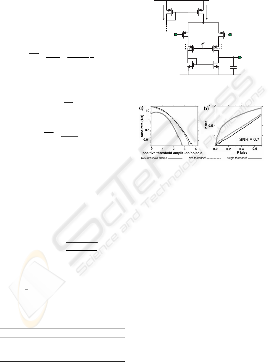
the comparator triggers a time-window generator, de-
picted in Fig. 5. The output of the set-reset flip-
flop is normally in a low logic state (Q = 0), keep-
ing the capacitor charged. When a positive peak of
AP is detected, the NMOS swiftly discharges the ca-
pacitor and the resulting drop of the transistor drain
voltage turns off the same NMOS, thus enabling the
capacitor re-charging. When the recharging capaci-
tor voltage crosses the trigger threshold, the cycle is
repeated. This block acts then as a clock generator,
feeding the counter that generates the output, namely
the time window. When the counter completes its cy-
cle, it resets the flip-flop, bringing everything to the
initial state. The current I
CHARGE
can be externally
tuned in order to produce time windows of different
lengths. For example, by setting I
CHARGE
= 20 nA
we obtain a time window of 1 ms with a 10 pF ca-
pacitor. The second signal path has a low-pass filter
(implemented with a G
M
−C cell with tunable band-
width) followed by a second comparator with nega-
tive threshold V
L
. Finally, outputs of the two channels
feed a D-type flip-flop acting as an AND port: its out-
put is true only when a negative crossing happens dur-
ing the assertion of the time window. The following
parameters of the circuit were used for the tests here:
5 kHz for the low-pass filter, 0.6 for the ratio of the
two threshold amplitudes and about 2 ms for the time
window duration.
S
R
Q
Q
V
D D
- V
D D
C O U N T E R
E O C
C K
I
C H A R G E
C
P O S S P I K E
W I N D O W
Figure 5: Simplified schematic of the time-window genera-
tor.
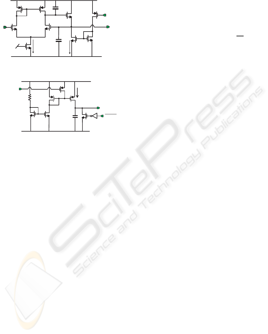
2.3 Spike-sorter Circuit
The amplified signal is also processed by a spike-
sorter block (see Fig. 1) that measures the peak and
the trough amplitudes and the width of the detected
spike. The peak detector circuit is shown in Fig 6(a).
If the ENABLE signal is low, the circuit acts as a tradi-
tional voltage follower, while when ENABLE is high
the source follower M
6
is biased with the small leak-
age current of transistor M
7
and it is able to follow
only the rising edge of the input signal. In the imple-
mented circuit, the ENABLE signal comes from the
time-window generator output: when the amplified
signal crosses the positive threshold, the time-window
signal is set high, forcing the detector to track the
peak. This control signal allows detecting peaks with
very different amplitudes and very close to each other,
that was not possible with the implementation in (Ho-
riuchi et al., 2004) because of the slow discharge after
a peak detection. Two aspects were taken into con-
sideration in the design of the peak detector. First,
the M
1
−M
4
amplifier gain was maximized (to about
50 dB) in order to reduce the detector offset (which
could cause a systematic error in the peak amplitude
evaluation). Second, the gate-source capacitance of
the follower transistor M
6
was minimized in order to
keep low the voltage drop caused by the input voltage
that drops below the peak voltage.
The trough detector is the PMOS equivalent of the
Fig 6(a) circuit. In this case, the enable signal for the
trough detector is the spike-detector output itself.
The width detector circuit, shown in Fig. 6(b), is a
time-to-amplitude converter, based on the charging of
a capacitor with a constant current, with two control
signals, ENABLE and RESET. The latter is the time-
window signal (TIME WINDOW), while ENABLE is
the logic exclusive OR between TIME WINDOW and
SPIKE DET. The crossing of the positive threshold
activates the current generator, M
5
, and switches off
M
6
. The capacitor C = 10 pF is charged by a 30 nA
constant current until the crossing of the negative
BIODEVICES 2009 - International Conference on Biomedical Electronics and Devices
70
V
D D
= + 1 . 5 V
1
m
A
V
I N
C
C
P E A K
E N A B L E
C
P E A K
1
m
A
3 p F
5 p F
M
1
M
2
M
3
M
4
M
5
M
6
M
7
M
8
M
9
- V
D D
= - 1 . 5 V
(a) Peak detector
R E S E T
W I D T H
E N A B L E
1 0 p F
M
1
M
2
M
3
M
4
M
5
M
6
3 0 n A
V
D D
= + 1 . 5 V
- V
D D
= - 1 . 5 V
(b) Width detector
Figure 6: Simplified schematic of the peak detector (a) and
width detector (b).
threshold. Then, the capacitor voltage is kept constant
to a value proportional to the time between the posi-
tive and the negative threshold crossing, until the time
window signal goes down discharging the capacitor.
The gain of the width detector is about 3 V/ms. Note
that all the three sorter output signals (peak, trough
and width signals in Fig. 1) are meaningful only when
the spike detector output is high. If a spike is de-
tected, both the falling edge of the TIME WINDOW
signal and of the SPIKE DET signal reset the three
spike sorter outputs meaning that the SPIKE DET sig-
nal may be used as a trigger for read-out of the analog
sorter outputs in order to convert these signals into a
digital format.
3 CIRCUIT TEST
A test structure with a pre-amplifier, a spike detec-
tion circuit and an analog sorter was implemented
in 0.35-µm AMS CMOS process occupying a total
area of 0.24 mm
2
(see Fig. 7). The LNA was char-
acterized using an HP35665A Dynamic Signal Ana-
lyzer. The measured transfer function is presented in
Fig. 8, showing a mid-band gain of 71.5 dB and a
29 Hz−22 kHz pass-band. The same figure shows the
transfer function of the LNA followed by the G
M
−C
filter present in the trough path of the spike detector.
The upper cut-off frequency is set to about 5 kHz
by tuning the bias current of the G
M
−C low-pass
cell. The measured input-referred noise power spec-
trum is shown in Fig. 9. It was obtained by divid-
ing the output noise power spectral density by the
square of the overall transfer function. The input-
referred thermal noise is about 25 nV/
√
Hz, as ex-
pected for the set bias current, while the noise cor-
ner frequency is about 800 Hz, higher than the esti-
mated value. This result is likely to be due the incor-
rect model of the flicker noise for a transistor working
in the weak-inversion/subthreshold region, that is the
case for the input PMOS transistors. Integrating the
input-referred noise spectrum over the pre-amplifier
band, we get a 4 µV
rms
input noise, while the mea-
sured current consumption is 4.7 µA for the first stage
LNA and 0.5 µA for the operational amplifier in the
second stage. The Noise Equivalent Factor (NEF) of
the LNA is 2.45 which is the best result reported to
date (Fig. 10). However, this NEF is higher than the
theoretical limit obtained in the previous section, due
to the presence of the unaccounted flicker noise and
of a second amplification/filtering stage. The spike
detection block was tested with simulated APs sig-
nals immersed in a realistic background noise fed into
the integrated circuit using a TTI TGA12104 arbitrary
waveform generator. Fig. 11 shows the amplified ar-
tificial neural activity, the control signals that trigger
the spike detector (output of positive- and negative-
threshold comparators) and the spike detector out-
put itself. Note the false-positive threshold crossing
shown in figure: a simple threshold algorithm would
interpret it as a true spike firing event, while our algo-
rithm rejects it correctly, thus increasing the detection
reliability. The current consumption of the spike de-
tector is largely determined by the comparators (each
one draws 2 µA), and by the time window generator.
The latter dissipates only when the positive threshold
is crossed and in the case of 100 Hz firing rate, the
average current consumption is 10 µA. The G
M
−C
filter has a negligible current consumption since its
bias current is about 0.1 µA. In addition, to verify
the correct measurement of the three features (peak,
trough and width amplitudes) for detected spikes, the
spike sorter circuit was tested with simulated wave-
forms. The amplified trace was recorded as well as
peak, trough and width outputs of the spike sorter. A
snapshot of the measured signals is shown in Fig. 12.
The three features measured by the spike sorter were
compared with the same features extracted from the
acquired LNA output using MATLAB
R
. For ampli-
fied spikes of 400 mV peak amplitude the error was
never larger than 30 mV. This value corresponds to
an error of 8 µV for a 106 µ V peak amplitude input
A LOW-POWER INTEGRATED CIRCUIT FOR ANALOG SPIKE DETECTION AND SORTING IN NEURAL
PROSTHESIS SYSTEMS
71
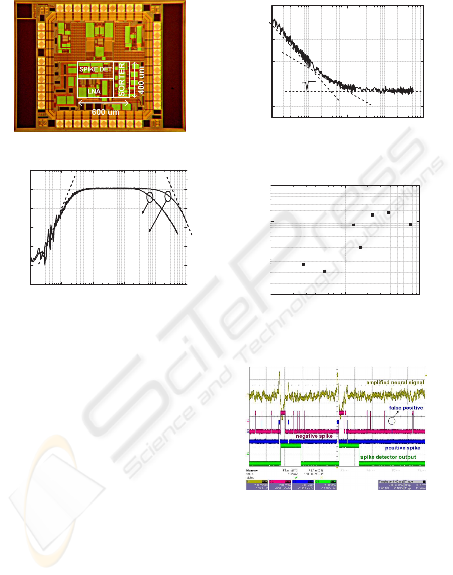
Figure 7: Die photo of the proposed circuit.
1 10 100 1k 10k 100k
20
30
40
50
60
70
80
only LNA
-40dB/dec
+40dB/dec
LNA + G
M
-C filter
Transfer Function [dB]
Frequency [Hz]
Figure 8: Measured transfer functions for the LNA ampli-
fier (22-kHz bandwidth) and for the LNA + G
M
−C filter
(5-kHz bandwidth).
spike. In the same way we obtained a maximum error
of 50 µs for a spike width of 500 µs. The power con-
sumption of the spike sorter block was kept very low:
the peak and the trough detector draw 2 µA each while
the width detector has a negligible consumption. The
power dissipation of the whole system (output buffers
excluded) is about 70 µW fora 3-V power supply. The
main characteristics of the whole circuit are summa-
rized in Table 2.
4 TEST WITH SIGNALS
To test the efficiency of the spike sorter, we used a
variety of traces obtained during in-vivo recordings in
monkeys employing tungsten electrodes (impedance
in the range of 0.5 −2 MΩ). The signals were down-
loaded to the waveform generator and then fed into
the IC through an attenuation filter to simulate the
real amplitude of the neural signal and the input re-
sistance of typical electrodes. For AP detection and
sorting, the peak threshold was set to about 4 times
the standard deviation of the background noise while
10 100 1k 10k 100k
-160
-150
-140
-130
-120
1/f
2
25nV/ Hz
1/f
Input Referred Noise [V
2
/Hz]
Frequency [Hz]
Figure 9: Measured input-referred noise spectrum of the
LNA.
1 10 100
0.1
1
10
100
[Harrison, 2003]
[Perelman, 2007]
[this work]
[Olsson, 2005]
[Mohoseni, 2004]
[Harrison, 2007]
[Wattanapanitch, 2007]
NEF - theoretical limit
Current Consumption [uA]
Figure 10: Difference between measured NEF and mini-
mum theoretical limit (2.02) of published neural differen-
tial amplifiers as a function of the supply current.
Figure 11: Snapshot of measured signals. From top to bot-
tom: LNA output signal, outputs of the comparator with
negative and positive threshold and spike detector output.
the trough detector threshold was 0.6 times the peak
threshold. All these tests yielded similar results, so
that here we only describe a typical case obtained with
an in vivo recording trace (see Fig. 13). We compared
the chip sorted waveforms with the results obtained
employing the Principal Components (PCs) analysis
of AP waveforms and identifying clusters of events
in the space of the three largest PCs (Lewicki, 1998).
BIODEVICES 2009 - International Conference on Biomedical Electronics and Devices
72
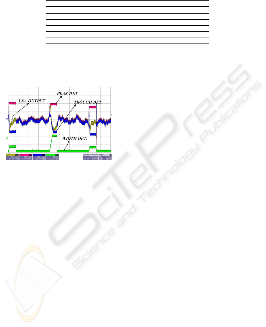
Table 2: System electrical characteristics.
Technology CMOS 0.35−µm AMS
Amplifier + spike-detector + spike sorting area 0.24 mm
2
Power supply 3.0 V
Pre-amplifier midband gain 71.5 dB
Pre-amplifier bandwidth 29 Hz−22 kHz
Pre-amplifier input noise (29 Hz−22 kHz) 4 µV
rms
Overall pre-amplifier NEF 2.45
Current consumption (output buffers excluded)
Pre-amplifier (1
st
stage) 4.7 µA
Pre-amplifier (2
nd
stage) 0.5 µA
Spike detector (for a 100 Hz firing rate) 14.1 µA
Spike sorter 4.1 µA
Total 23.4 µA
Figure 12: Snapshot of the measured signals of the ana-
log sorter: amplified neural signal (gold line), peak detec-
tor output (red line), trough detector output (blue line) and
width detector output (green line).
In this case, the AP waveforms were obtained by de-
tecting the events of threshold crossing and collect-
ing about 0.3 ms of trace before and 1.3 ms after
the event. Since we used real data, there is no as-
surance that AP shapes are sorted correctly. There-
fore, to asses the quality of unit separation, we used
AP occurrence auto- and cross- correlograms (Har-
ris et al., 2000). The method is based on the fact that
each neuron has a certain refractory period of 2−3 ms
after firing an AP during which no spike can be gen-
erated. Thus, if all AP shapes are derived from a sin-
gle neuron, there should be no APs occurring at in-
tervals less than the refractory period of the neuron.
This absence of APs at brief intervals will correspond
to no events around the midpoint (0 ms interval) in
the auto-correlogram (Fig. 13). In the case of a pure
noise signal, the probability to detect events around
the midpoint (i.e.: events separated by small time in-
tervals) would be equal to the probability of detect-
ing events separated by large time intervals. Thus,
by comparing the frequency of events at very short
and very long intervals it is possible to estimate the
quality of the achieved unit separation. In the ex-
ample shown in Fig. 13, both methods were able to
detect two units and the remaining events turned out
to be noise. While in the PCA analysis both units
have clean refractory periods with no events for inter-
vals of < 3 ms, the chip separated units have a small
background noise (Fig. 13). However, compared to
the large interspike intervals, the frequency of these
short interspike interval events was very low (< 10
fold) suggesting that less than 10% of identified units
were misclassified. Similarly, the number of events
detected by our spike sorter was > 90% of the ones
detected by PCA analysis confirming that our simple
sorter is able to achieve 90% efficiency of the PCA
analysis method. Similar results were obtained with
the simulated test signals downloaded from the public
database (
http://www.vis.caltech.edu/
˜
rodri/
Wave_clus/Waveclus_home.htm
, data not shown)
thus confirming the conclusions reached with the real
signals.
5 CONCLUSIONS
The described analog integrated circuit for on-line AP
waveform separation was designed with intention to
be a part of a compact integrated multichannel sys-
tem where low power consumption, small size and
data compression/reduction are key factors to be con-
sidered during the systems design. The bandwidth re-
quired to transmit the three AP features depends on
the neurons firing rate. For a typical electrode signal
containing 2 −3 neurons firing rate at < 50 Hz, and
with 10 bits of resolution, the estimated bandwidth to
transmit one channel data processed by our device or
less than 4 −5 kbps. Thus, information contained in
100 channels can be wireless transmitted with a de-
vice capable of 500 kbps data rates that is well within
the range of current state of the art systems. The three
features selected to perform the discrimination of dif-
ferent spikes were proved to work with real signals.
Our implementation overcomes some of the problems
A LOW-POWER INTEGRATED CIRCUIT FOR ANALOG SPIKE DETECTION AND SORTING IN NEURAL
PROSTHESIS SYSTEMS
73
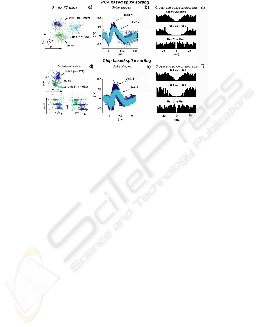
Figure 13: Comparison of PCA- and chip-based spike sorting. a) Unit 1 and 2 and noise plotted in the PCA space.
b)Waveforms of single units. c) Cross- and auto-correlograms of waveforms selected with PC analysis. d) Single wave-
forms plotted in the chip-extracted three dimension space of features. Isolated clusters are clearly visible. e) Single units’
waveforms assigned by employing the chip-based sorting. f) Cross- and auto-correlograms of the single units identified with
the chip-based sorting method.
of similar systems, such as a slow recovery of peak
detectors after sensing an AP (Horiuchi et al., 2004),
while remaining an extremely low-power circuit with
overall power density of (< 300 µW/mm
2
) that makes
this circuit suitable for multichannel implantable sys-
tems.
ACKNOWLEDGMENTS
The authors would like to thank M. L. Grossi for her
help in the circuit design. This work was partially
supported by IIT (Italian Institute of Technology) and
by EC funds to LF (RobotCub IP).
REFERENCES
Harris, K., Henze, D., Csicsvari, J., Hirase, H., and Buzsaki,
G. (2000). Accuracy of tetrode spike separation as
determined by simultaneous intracellular and extra-
cellular measurements. Journal of Neurophysiology,
84:401–414.
Harrison, R. and Charles, C. (2003). A low-power low-
noise cmos amplifier for neural recording applica-
tions. IEEE J. Solid-State Circuit, (6):958–965.
Harrison, R. R., Watkins, P. T., Kier, R., Lovejoy, R., Black,
D. J., Greger, B., and Solzbacher, F. (2007). A low-
power integrated circuit for a wireless 100-electrode
neural recording system. IEEE J. Solid-State Circuit,
(1):123–133.
Hochberg, L., Serruya, M., Friehs, G., Mukand, J., Saleh,
M., Caplan, A., Branner, A., Chen, D., Penn, R., and
Donoghue, J. (2006). Neuronal ensemble control of
prosthetic devices by a human with tetraplegia. Na-
ture, (442):164–171.
Horiuchi, T., Swindell, T., Sander, D., and Abshier, P.
(2004). A low-power CMOS neural amplifier with
amplitude measurements for spike sorting. In Pro-
ceedings of ISCAS, pages 2932–2395.
Lewicki, M. (1998). A review of methods for spike sort-
ing: the detection and classification of neural action
potentials. Network: Computation in Neural Systems,
9(4):53–78.
Olsson, R. and Wise, K. (2005). A three-dimensional
neural recording microsystem with implantable data
compression circuitry. IEEE J. Solid-State Circuit,
(40):2796–2804.
Olsson, R. H., Buhl, D. L., Sirota, A. M., Buzsaki, G.,
and Wise, K. D. (2005). Band-tunable and multi-
plexed integrated circuits for simultaneous recording
and stimulation with microelectrode arrays. IEEE
Trans. Biomed. Eng., 52:1303–1311.
Stieglitz, T. (2007). Neural prostheses in clinical practice:
biomedical microsystems in neurological rehabilita-
tion. Acta Neurochir Suppl, 97:411–418.
Vibert, J. and Costa, J. (1979). Spike separation in multiu-
nit records: a multivariate analysis of spike descrip-
tive parameters. Electroenceophal. Clin. Neurophys.,
(47):172–182.
Wattanapanitch, W., Fee, M., and Sarpeshkar, R. (2007).
An energy-efficient micropower neural recording am-
plifier. IEEE Trans. Biomed. Eng., 1(2):136–147.
BIODEVICES 2009 - International Conference on Biomedical Electronics and Devices
74
