Fault Modeling of Implantable MEMS Sensors
J. A. Miguel
1
, Y. Lechuga
1
, M. Martinez
1
and J. R. Berrazueta
2
1
Microelectronics Group, TEISA Department, University of Cantabria, Avda de los Castros s/n, Santander, Spain
2
Department of Medicine, Faculty of Medicine, University of Cantabria, Avda de Valdecilla s/n, Santander, Spain
Keywords: MEMS Testing, Fault Injection, Biomedical Transducers, Implantable Biomedical Devices, Cardiology.
Abstract: The aim of this work is to analyse the fault-injection problem of implantable capacitive micro-electro-
mechanical pressure sensors intended to be used as a part of smart stents for in-stent restenosis monitoring.
The development of accurate fault models is mandatory in order to create a Design-for-Test methodology
compatible with MEMS-based sensors as well as with its related CMOS electronic circuitry. Rigorous
behavioural descriptions of both circular and square-shaped fault-free pressure sensors can be obtained from
analytical expressions and numerical approximations. However, the deflection vs. pressure response of
faulty sensors, suffering from contamination-based defects growth during the fabrication process, require
the use of finite-elements analysis to be modelled, allowing the fulfilment of a realistic fault model library.
1 INTRODUCTION
During the last decade, the fast development of
Micro-Electro-Mechanical Systems (MEMS), in
conjunction with the build-up of new fabrication
technologies compatible with CMOS processes has
made possible the production of heterogeneous
systems, integrating MEMS structures and electronic
circuits on the same silicon substrate. In this way, a
miniaturization of implantable electronic devices has
been achieved, increasing their capabilities and uses.
Nowadays, Atherosclerosis, affecting cardiac,
cerebral, renal or peripheral vascular vessels, is the
most prevalent disease in developed countries,
responsible for nearly 47% of deaths in Europe. The
related treatment costs reach about 9% of the total
healthcare expenditure from countries across the EU,
with inpatient hospital care comprising 49% of these
costs (Nichols et al., 2012).
Percutaneous Coronary Interventions (PCI),
allow an accurate diagnosis of obstructive lesions
using arteriography, as well as a reliable treatment
through balloon angioplasty, generally accompanied
by stenting. In Spain, nearly 124.000 diagnostic
coronary angiograms are performed annually. In
66.000 of these cases an angioplasty is performed,
and in 55.000 cases 100.000 stents are implanted,
trying to avoid restenosis, the most important
sequela of this technique (Garcia B. et al., 2013).
Severe and symptomatic carotid lesions have a
similar treatment by neuroradiologists. In general
population, total severe carotid stenosis is estimated
in less than 1%. However the prevalence of lesions
greater than 50% in population younger than 70
years is 4.8% in men and 2.2% in women, rising to
12.5% for males and 6.9% for women over 70 years
(Wolff T. et al., 2007).
The prevalence of lower extremity Peripheral
Artery Disease (PAD) ranges from 3% to 12%, with
202 million people affected in 2010 (Fowkes F.G. et
al., 2013). The annual incidence of critical ischemia
of the lower extremities varies from 500 to 1.000
new cases per million population, being higher for
patients with diabetes (Tendera M. et al., 2011).
During angioplasty, a flexible balloon catheter is
threaded into the blockage location and inflated,
applying a controlled pressure which compresses the
plaque deposition against the artery walls.
Angioplasty is usually accompanied by stents placed
surrounding the tip of the balloon catheter. Once the
balloon tip is inflated, the stent spring is opened and
attached to the vessel walls, remaining in place after
the balloon is deflated and removed. Thus, the stent
holds the vessel open, lessening the risk of re-
narrowing due to elastic recoils and spasms.
However, In-Stent Restenosis (ISR), a process of
neointimal tissue growth inside the stent, supposes a
major drawback to angioplasty reliability.
ISR monitoring is carried out nowadays using
expensive techniques, like angiography and
intravascular ultrasound. Smart stents, implantable
electronic devices able to sense and transmit real-
162
A. Miguel J., Lechuga Y., Martinez M. and R. Berrazueta J..
Fault Modeling of Implantable MEMS Sensors.
DOI: 10.5220/0005278801620167
In Proceedings of the International Conference on Biomedical Electronics and Devices (BIODEVICES-2015), pages 162-167
ISBN: 978-989-758-071-0
Copyright
c
2015 SCITEPRESS (Science and Technology Publications, Lda.)

time data from physiological signals related to the
vessel condition, have positioned themselves as an
economic alternative to ISR follow-up.
Smart stents, as implantable electronic devices,
must fulfil certain design constraints, including
small size, low power requirements, output stability,
and reliability over time without recalibration. This
last challenge makes testing and fault modelling
critical issues to validate the fabricated device.
Generally, MEMS testing has been limited to a
set of electrical, optical and mechanical analyses,
used to check the functionality of the device.
However, the correlations between the detected
failures and their underlying physical causes are
usually missing. These relationships are needed to
allow an accurate modelling of complex fabrication
defects, and can be useful in the generation of
realistic faults models, as well as in the development
of capable testing techniques. For this reason, fault
models must include real defective behaviours in
order to reach high fault coverage and test quality.
This work focuses on the generation of a fault
model for an implantable MEMS capacitive pressure
sensor. Finite Elements (FE) tools have been proven
to be necessary to model those faults whose
complexity makes analytical descriptions inapt. The
results from FE analysis will give rise to a realistic
fault model library, and to the development of a
comprehensive Design-for-Test (DfT) methodology.
In Section 2, the most common failure
mechanisms affecting MEMS devices are described.
Section 3 introduces the proposed heterogeneous
system, focusing on the analytical modelling of its
MEMS sensors under fault-free conditions. Section
4 illustrates the need of FE analysis to model the
behaviour of MEMS sensors under the presence of
certain faults. Finally, in Section 5 conclusions are
presented.
2 MEMS FAULT CLASSES AND
FAILURE MECHANISMS
Several failure mechanisms or defects can appear
during the fabrication process of heterogeneous
devices, being possible to distinguish between
defects arising during the CMOS process and defects
occurring during micromachining.
Microelectronic and MEMS components can be
created on the same silicon substrate by means of a
set of conductor, semiconductor and dielectric
layers. Each one of the technological operations
used to grow these layers, such as oxidation,
deposition, photolithography or etching, is a
potential source of defects, where contaminants can
appear, degrading the succeeding fabrication steps.
In the particular case of CMOS-compatible
MEMS, failure mechanisms can be classified
according to the physical property being affected.
MEMS faults can be initially grouped into
parametric or catastrophic types, in the same way as
for analog testing. However, the nature of MEMS
devices gives rise to new types of manufacturing
defects, which require an extended classification
scheme. Thus, it is necessary to distinguish between
faults affecting the microsystem gauge and those
affecting the supporting structure. Each of these
faults can be again classified as a parametric fault,
changing the physical properties of the device and
altering its performance; or as a catastrophic fault,
preventing any use of the system.
In this work, the case of impurities appearing
during the anisotropic wet etching process used to
create diaphragms is analysed in detail. Impurities in
the form of small crystal lattice defects located in the
bulk material during this process can cause the
growth of pyramids on top of the diaphragm.
Depending on their size and location, these pyramids
can strongly change the properties of the diaphragm.
As can be seen in Fig. 1, the sidewall slope of the
pyramids is a fixed parameter which depends on the
angles between the main crystal planes of a single
silicon crystal. For instance, this slope presents a
value of 54.7º in the case of anisotropic wet etching
of a {100} oriented wafer, corresponding to the
angle between the {100} and {111} planes. It must
be noticed that the height of the pyramid can be
obtained from the sidewall slope, so a change in the
base length of the pyramid will alter its size (Rosing,
Reichenbach, Richardson, 2002) (Landsberger,
Nashed, Kahrizi, Paranjape, 1996).
Figure 1: Pyramid defect growth during anisotropic wet
etching process.
3 MEMS PRESSURE SENSOR
MODELLING
One of the simplest and more reliable smart stent
FaultModelingofImplantableMEMSSensors
163

designs for ISR monitoring is made up of two
MEMS capacitive pressure sensors attached at
opposite sides of a regular stent. In this way, the
pressure gradient along the device (implanted in a
distal pulmonary artery) can be measured and
wirelessly transmitted outside the patient body by
means of an LC tank formed by the sensors and the
body of the stent (Takahata, Gianchandani, Wise,
2006).
The proposed MEMS capacitive pressure sensor
to be included in the above-mentioned smart stent
can be split into two different parts: a fully-clamped
suspended flexible top diaphragm anchored to the
substrate, and a fixed back plate. The principle of
operation governing the behaviour of this kind of
sensors is based on the concept of a two parallel
plate capacitor, where the resultant capacitance is
inversely proportional to the distance between the
plates.
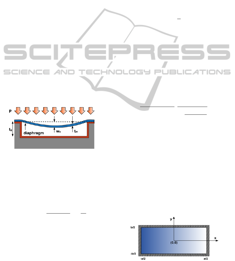
Fig. 2 shows a simplified cross-sectional view of
a MEMS capacitive pressure sensor with an air-
filled cavity. When a certain pressure P is uniformly
applied to the top plate, with a thickness t
m
, a
deflection is induced, reducing the initial gap t
g
between the plates and increasing the sensor
capacitance. The parameter w
0
refers to the
maximum deflection of the plate.
Figure 2: Cross-sectional view of a MEMS capacitive
pressure sensor.
The equivalent capacitance of a MEMS pressure
sensor can be analytically calculated by the
expression stated in (1), where C
0
is the capacitance
of the undeformed sensor, ε
0
is the dielectric
permittivity of the void, and A is the overlapped area
between both plates.
g
0
A
g
0
0S
t
A
ε
y)w(x,-t
dydxε
CCΔC
(1)
3.1 Circular Sensor
An analytical behavioural modelling of a fully-
clamped diaphragm can be achieved only when
certain conditions are fulfilled: (a) the fabrication
material of the top diaphragm must have isotropic
mechanical properties; (b) the thickness of the
metallic electrode on the top plate is required to be
smaller than the thickness of the plate in order to be
neglected; (c) the initial gap between the plates must
be small compared to the lateral extents of the
plates, so that the influence of the field fringing
effects could be neglected; (d) the residual stresses
in the flexible diaphragm are not considered. Once
all the requirements have been met, the plate
deflection at radius r, of a fully clamped circular
diaphragm, can be expressed as:
2
2
0
a
r
1ww(r)
(2)
Where r is the distance of the point of interest to
the centre of the diaphragm, a is the radius of the
diaphragm and w
0
is the maximum centre deflection.
Depending on the sensor deflection-to-thickness
ratio, the maximum centre displacement can be
analytically modelled using different expressions, as
described in (Timoshenko, Woinowsky-Krieger,
1959). The centre displacement vs. pressure
relationship for both small and large deflection
conditions can be approximated as (Timoshenko,
Woinowsky-Krieger, 1959):
2
m
2
0
3
m
24
0
t
w0.488
1
1
tE16
ν1aP3
w
(3)
Where P is the pressure applied to the
diaphragm, a is its radius, and υ and E are the
Poisson’s ratio and Young’s modulus of elasticity of
the diaphragm material respectively.
3.2 Rectangular Sensor
The deflection of a rectangular flexible diaphragm,
as shown in Fig. 3, can be analytically modelled by a
set of differential equations (4) and (5). Some
conditions have to be fulfilled to validate the model:
(a) the diaphragm must be fully clamped at its edges;
(b) the bending of the diaphragm must be elastic; (c)
the deflection has to remain smaller than half the
thickness of the diaphragm.
Figure 3: Coordinate system of a rectangular diaphragm.
BIODEVICES2015-InternationalConferenceonBiomedicalElectronicsandDevices
164

Thus, the fully clamped rectangular diaphragm
deflection vs. pressure relationship can be
approximated by the following differential equation
and its boundary conditions:
3
m0
4
4
42
4
4
4
tD
P
y
w
yx
w
2
x
w
(4)
0
2
b
y;x
x
w
0;y
2
a
x
x
w
0
2
b
y;xw
0;y
2
a
xw
(5)
Where
E
)υ1(E2
υα
2
t
(6)
)υ1(12
E
D
2
0
(7)
and a, b, E, E
t
and υ are the diaphragm x-length
and y-length, the Young’s elasticity modulus, the
shear modulus and Poisson’s ratio, respectively.
The following changes in variable are introduced
to limit the integration domain to a square of unit
side:
1Y1;
b
y2
Y
1X1;
a
x2
X
(8)
The system of differential equations can be
approximated via several mathematical methods.
The Galerkin method has been applied
(Timoshenko, Woinowsky-Krieger, 1959), leading
to the following analytical result:
)r,Y,X(fw)P,y,x(w
0
(9)
P
tD16
bak(r)
w
3
m0
22
0
(10)
n
0i
n
0j
ji
ij
2
22
Y(r)Xk)Y)(1X(1
r)Y,f(X,
(11)
Where n is an even positive integer; i, j=0, 2, 4,
6, …, n; r=b/a; k(r) and k
ij
(r) are tabulated shape
factors, whose values are shown in Table 1.
Table 1: Coefficients of the polynomial solution for a
rectangular fully clamped diaphragm.
r 1 2 3
k(r) 0.02019 0.01035 0.00469
k00 1 1 1
k20 0.233 0.01837 0.00510
k02 0.233 1.27 1.82
k22 0.252 0.195 -0.183
k40 -0.00166 -0.00253 -0.00033
k04 -0.00166 0.475 3.030
k42 0.13 0.00181 0.0306
k24 0.13 0.636 1.46
k44 -0.235 0.0495 0.0844
3.3 Results Comparison
A behavioural model for circular and square
diaphragms has been developed based on the
previously-mentioned analytical expressions. Both
sensors have been designed to present identical
capacitance for zero pressure difference between the
sealed cavity and the environment surrounding the
device.
The sensors are based on PolyMUMPs
technology provided by MEMSCAP. The diaphragm
is made of polysilicon (Young Elasticity Modulus:
E=169GPa; Poisson’s ratio: υ=0.22) with a thickness
of 4µm, and a 2µm gap between the plates, filled
with air sealed at ambient pressure. The circular
sensor presents a radius of 350µm, while the square-
shaped sensor has a side length of 620.35µm.
Pressures up to 60mmHg have been simulated,
corresponding to conditions of moderate stenosis.
These two sensors have been modelled in Ansys
®
. In
this way, it is possible to compare results from
analytical and FEA simulations, as shown in Fig. 4.
It can be noticed that in the case of a square sensor,
the error induced by the analytical formulation is
proportional to the pressure. This is explained
considering the numerical approximation used to
Figure 4: Analytical vs. FEA centre deflection response
for circular and square-shaped diaphragms.
FaultModelingofImplantableMEMSSensors
165

solve the differential equation in (4), so a certain
deviation is inevitable. Other numerical methods can
be used to enhance the accuracy of the model, at the
expense of higher complexity and computing times.
4 FE FAULT INJECTION
A complete library of accurate fault models, based
on real defects, needs to be developed to enable fault
simulations with a realistic estimation of the fault
coverage of the test method. The use of FE tools is
proposed to analyse the influence of defects
occurring during the fabrication or the lifetime of the
sensor. The detection and description of defects that
give rise to faults will ease the generation of an
electrical-compatible behavioural model where new
test methodologies could be evaluated.
In this case, FE models of fully-clamped circular
and square diaphragms have been built in Ansys
®
.
Defects with different sizes and locations have been
inserted on the top plate, where a uniformly
distributed pressure is applied. For each particular
fault, the capacitance and centre deflection are
measured, enabling the evaluation of their influence.
Pyramids grown during the anisotropic wet
etching process have been chosen as the case under
study. Fig. 5a and Fig. 5b show the capacitance
results for circular and square sensors respectively,
with pyramids of base areas up to 2500 µm
2
located
at the centre of their diaphragms. As expected, the
influence of a pyramid is proportional to its size,
with bigger pyramids compromising the reliability
of the sensor due to strong sensitivity losses. It can
be noticed that the sensitivity loss is higher for
circular plates (8.77% loss for a 50x50µm
2
pyramid)
than for their square counterparts (4.8% loss). In Fig
6a and Fig. 6b the capacitance results for both
sensors, under the influence of a pyramid of 50µm
base side placed at different locations, are shown. In
a fault-free case, the centre and anchoring locations
of a circular plate present the maximum bending
conditions. On the other hand, a square diaphragm
has its critical stress density spots located at its
centre, at its side midpoint (θ=0º) and at the
midpoint of the semi-diagonal of the plate (θ=45º).
The presence of rigid pyramids at these locations
prevents any bending of the plate, reducing the
sensitivity of the sensor.
In order to probe the accuracy of the simulation
results, several prototype PolyMUMPs capacitive
pressure sensors have been designed and fabricated.
These sensors have been conceived to be part of an
ISR monitoring smart stent device, designed to be
Figure 5a: Capacitance vs. pyramid base area: circular
sensor.
Figure 5b: Capacitance vs. pyramid base area: square
sensor.
Figure 6a: Capacitance vs. pyramid location: circular
sensor.
Figure 6b: Capacitance vs. pyramid location: square
sensor.
implanted in a distal ramification of the pulmonary
artery. Hence, the sensors must be capable of
bearing pressure ranges between light (Pmin =
30mmHg) to moderate (Pmax = 60mmHg) stenosis
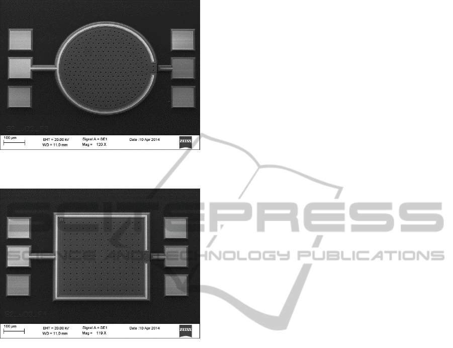
conditions. Both fault-free (Fig. 7) and fault-injected
(Fig.8) sensors have been fabricated, and are
expected to be measured under in-vitro conditions
once coated with the biocompatible materials.
BIODEVICES2015-InternationalConferenceonBiomedicalElectronicsandDevices
166

Figure 7: SEM picture of a fault-free PolyMUMPs circular
capacitive pressure sensor.
Figure 8: SEM picture of a fault-injected PolyMUMPs
square capacitive pressure sensor (injected fault located on
the top left corner of the sensor).
5 CONCLUSIONS
In this work, fault modelling problems affecting
MEMS capacitive pressure sensors for ISR detection
have been analysed. The most common failure
mechanisms and defects that generate faulty
behaviours have been introduced.
The deflection modelling of circular and
rectangular diaphragms has been proven to be
solvable via analytical expressions and numerical
approximations for the fault-free case. However,
these mathematical methods are no longer valid to
describe the behaviour of MEMS sensors under
certain faulty conditions, where their material
properties and geometry are affected. In order to
obtain a realistic fault model in all these cases, the
use of FE tools is required.
The development of a realistic fault model
library, as well as a comprehensive MEMS testing
approach, depends on the methodology extension of
to any other faulty conditions detected during
MEMS fabrication process and its useful lifetime.
REFERENCES
Nichols M. et al., Cardiovascular Disease Statistics 2012,
European Heart Network, Brussels. European Society
of Cardiology, Sophia Antipolis, 2012.
Garcia Blanco B. et al., Spanish Registry on Cardiac
Catheterization and Interventional Cardiology: XXII
Official Report of the Working Group on Cardiac
Catheterization and Interventional Cardiology of the
Spanish Society of Cardiology (1990-2012), Revista
Española de Cardiología, vol. 66, pp. 894-904, 2013.
Wolff T. et al., Screening for carotid artery stenosis: an
update of the evidence for the US Preventive Services
Task Force, Annals Internal Medicine, vol. 147,
pp.854-859, 2007.
Fowkes F.G. et al., Comparison of Global Estimates of
Prevalence and risk factors for peripheral artery
disease in 2000 and 2010: a systematic review and
analysis, Lancet, vol. 382, pp. 1329-1340, 2013.
Tendera M. et al., ESC Guidelines on the diagnosis and
treatment of peripheral artery diseases. Document
covering atherosclerotic disease of extracranial carotid
and vertebral, mesenteri, renal, upper and lower
extremity arteries: the Task Force on the Diagnosis
and Treatment of Peripheral Artery Diseases of the
European Society of Cardiology (ESC), European
Heart Journal, vol. 32, pp. 2851-906, 2011.
Rosing R., Reichenbach R., Richardson A., Generation of
component level fault models for MEMS,
Microelectronics Journal, vol. 33, pp. 861-868, 2002.
Landsberger L. M., Nashed S., Kahrizi M., Paranjape M.,
On Hillocks Generated During Anisotropic Etching of
Si in TMAH, Journal of Microelectromechanical
Systems, vol. 5, no. 2, pp. 106-116, 1996.
Takahata K., Gianchandani Y. B., Wise K.D.,
Micromachined antenna stents and cuffs for
monitoring intraluminal pressure and flow, Journal of
Microelectromechanical Systems, vol 15(5), pp. 1289-
1298, October 2006.
Timoshenko S., Woinowsky-Krieger S., Theory of Plates
and Shells, McGraw-Hill, New York, 1959.
FaultModelingofImplantableMEMSSensors
167
