
New Maskless Lithography System for Fabricating Biodevices using
Light-Emitting Diodes and Squared Optical Fibers
Jun Watanabe, Jun-ya Iwasaki and Toshiyuki Horiuchi
Tokyo Denki University, 5 Senju-Asahi-cho, Adachi-ku, Tokyo 120-8551, Japan
Keywords: Light-Emitting Diode, Squared Optical Fiber, Projection Exposure, Biodevice, Cell Array, Micro-Fluidic
Path.
Abstract: A new low-cost lithography system convenient for fabricating biodevices was developed. Using the new
system, various patterns of cell arrays, chamber arrays, flow paths of micro-fluidic devices, and others were
easily printed without preparing any reticles or masks. In the system, light-emitting diodes (LEDs) were used
as exposure sources and squared optical fibers arrayed in a 10×10 matrix were used as the combination of a
secondary light source and a reticle. Light rays emitted from each LED were individually led to each fiber,
and bright or dark of each LED was assigned by a personal computer. As a result, it became possible to print
arbitrary patterns without preparing any reticles or masks. In addition to the ordinary patterning using various
lightening maps of LEDs and their stitching, scan exposure was also tried. When bright images of optical
fiber ends were scanned on a resist film by moving the wafer stage, long patterns appropriate for micro fluidic
paths were very smoothly formed.
1 INTRODUCTION
Various researches are vigorously practiced for
supporting medical treatments and diagnosises, and
clarifying causes of diseases. As techniques or
procedures of such researches, chemical or medical
analysises using cell arrays and micro-fluidic devices
are frequently used. For example, functions of cells
and DNAs are often investigated. To speak about
researches on cells, for example, when and in what
state, what cells work and how to work are the
subjects (Arnandis et al., 2012; Choi et al., 2010; Kim
et al., 2013). It is often investigated what proteins are
made from particular DNAs also (Gach et al., 2014;
Schmidt et al., 2013). In such cases, it is important to
evaluate a lot of cell and DNA samples efficiently.
For this reason, in many cases, it is required to
develop special devices for analyzing them using
minute volume samples. Micro-chamber array chips
or micro-cell array chips are the most simple devices
for such usage (Bianchi et al., 2013; Lei et al., 2014).
That is, the micro-chambers or micro-cells work as a
lot of test tubes. Accordingly, by minimizing the sizes
of micro-chambers or micro-cells, it becomes
possible to reduce costs and analyzing time, and save
reagents. Micro-fluidic devices are also used for
analyzing various mixing and separation of small
quantity liquids (Wang and Hu, 2010).
As a fabrication method of such devices, optical
lithography is usually used (Boero et al., 2014; Ilyas
et al., 2014; Li et al., 2005; Malainou et al., 2012;
Moraes et al., 2010; Negrete and Cerrina, 2008; Tanii
et al., 2004). However, exposure systems for
lithography are very expensive even for printing very
large patterns with sizes of several tens or hundreds
microns. In addition, conventionally available mask
aligners and projection exposure systems with large
numerical apertures are not suitable for printing thick
resist patterns required for fabricating above
mentioned biodevice patterns. Because depth of focus
is generally small in such systems, it is difficult to
print thick resist patterns with almost vertical side
walls. In addition, because masks and reticles are also
expensive, it is not easy to change or improve pattern
shapes after once they are decided.
In this paper, a new exposure system is developed
using light-emitting diodes (LEDs) as exposure
sources. It has great advantages from the viewpoints
of cost and simplicity. Maintenance times are also
much reduced. In addition, optical fibers with squared
ends are developed, and the squared optical fibers
were bound in a matrix for printing smoothly stitched
patterns. Because bright or dark are directly assigned
by simply lighting and extinguishing LEDs, this
Watanabe, J., Iwasaki, J-y. and Horiuchi, T.
New Maskless Lithography System for Fabricating Biodevices using Light-Emitting Diodes and Squared Optical Fibers.
DOI: 10.5220/0005757802030208
In Proceedings of the 9th International Joint Conference on Biomedical Engineering Systems and Technologies (BIOSTEC 2016) - Volume 1: BIODEVICES, pages 203-208
ISBN: 978-989-758-170-0
Copyright
c
2016 by SCITEPRESS – Science and Technology Publications, Lda. All rights reserved
203
combination of LEDs and a fiber matrix is very
effective for easily printing arbitrary patterns as if
they are pixel arts without using any reticles. On the
other hand, it is also possible to print oblique and
curved patterns if the wafer stages are
programmatically scanned. It is demonstrated that
various patterns of biodevices are fabricated using the
exposure system.
2 NEW EXPOSURE SYSTEM
2.1 LED Exposure Optics
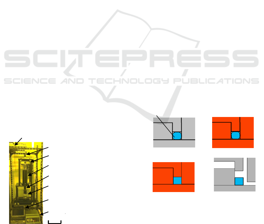
The newly developed exposure system is shown in
Figure 1. The sizes of the system were 600 mm wide,
400 mm deep, and 2,000 mm high. Bullet-type LEDs
with a central wavelength of 405 nm (OptoSupply,
OSSV5111A) were used as exposure sources, and
100 pieces of LED were attached to a universal board
in a 10×10 matrix. Assignments of ON or OFF were
given to all the LEDs using a personal computer.
Accordingly, arbitrarily designed patterns were
obtained without using reticles. The projected field
size was approximately 1×1 mm
2
, and the element
pattern size was 100×100 μm
2
because the projection
ratio was 1/10, and the squared fiber matrix size of
10×10 mm
2
was reduced by a factor of 10 through the
projection lens. The numerical aperture of the lens
was 0.4. Two-axis automatic stage (SIGMAKOKI,
SHOT202) was used as the wafer stage. The stage
was used for both step-and-repeat and scan exposures.
Ultra-high pressure mercury lamps are often used as
exposure sources in usual optical projection exposure
system. However, there is fear of lamp burst. In
addition, an expensive elliptical collector mirror is
Figure 1: Exposure system used for the research.
required. Without using these optical components, the
cost of exposure-source was much reduced.
2.2 Squared Optical Fiber
At the early stage of the past research, patterns were
printed directly using LEDs arrayed in a matrix.
However, because each LED had a strong intensity
distribution of emitted light, it was difficult to print
element patterns with a uniform shape. For this reason,
to obtain a uniform surface emission, optical fibers
were used. Collective-lens optics were designed and
inserted between each couple of an LED and a fiber.
In addition, to collect light rays emitted from LEDs
efficiently, plastic optical fibers (Mitsubishi Rayon,
Eska CK-40E1) with a diameter of 1 mm and clad
thickness of 10 μm were used. The end of each fiber
was transformed to a square shape in approximately
20 mm length from the fiber end. The sequence used
to deform circular optical fibers to square ones is
shown in Figure 2. First of all, an optical fiber was
inserted into a square clearance of a deforming
instrument and clamped using screws (a). The square
clearance was controlled to a size of 1×1 mm
2
. Next,
the instrument was heated at 150 °C on a hot plate for
5 min (b). Though the end part of the fiber heated in
the square space was expanded to fill the space, it
became shorter in the longitudinal direction. After
heating and deforming the fiber to a square cross
section, the fiber was cooled down in the instrument
(c), and taken out (d). Finally, the squared fiber end
was polished with emery papers. As a result, the cross
section of the optical fiber was deformed to a square,
as shown in Figure 3.
Figure 2: Method used for deforming optical fiber ends to
square shapes.
Optics for leading light rays from LEDs to
fibers through collective lenses
Fibers arrayed in 10×10 matrix
Shutter
1/10 projection lens
Wafer
Personal computer used for
exposure control
XYZ wafer stage
XY stage controller
200 mm
(c) Cooling
(d) Take out
(a) Clamping (b) Heating
Optical fiber
BIODEVICES 2016 - 9th International Conference on Biomedical Electronics and Devices
204
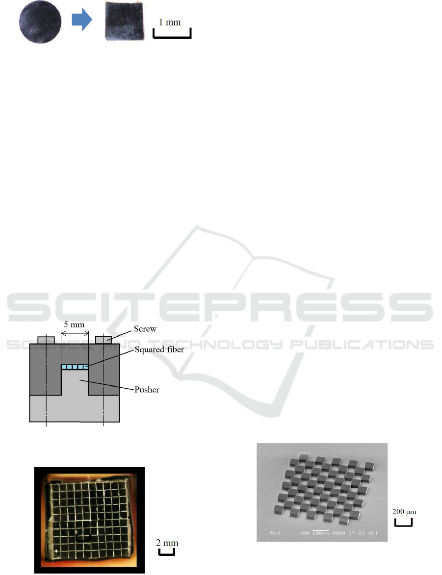
Figure 3: Fiber ends before and after squared.
2.3 Fiber Matrix
Sizes of all the squared fibers were measured using a
micrometer, and fibers with regular shapes and sizes
in a permissible range of within 1 ± 0.01 mm in both
vertical and horizontal directions were selected. Next,
the selected 5 optical fibers were simultaneously
inserted in a bundling instrument with a 5-mm
opening space, as shown in Figure 4, after coating
adhesive (Loctite LPP-005), and aligned in a line.
Such 5-fiber alignment and bonding were repeated
4times more. As a result, 5×5 fiber matrix was
obtained after the adhesive was hardened. 10×10
matrix was fabricated by bonding such 4 pieces of
5×5 matrices using the same adhesive, as shown in
Figure 5. The matrix end was polished again with
emery papers. Measured maximum gap between
fibers was 49 μm, and it was approximately 5% of the
square size. Accordingly, the maximum gap was
sufficiently small to use the fiber matrix as an
exposure tool.
Figure 4: Bundling instrument used for aligning and
bonding squared 5 fibers, and piling them.
Figure 5: Fibers arrayed in a 10×10 matrix and fixed to the
exposure system.
3 EXPERIMENTS
3.1 Patterning by using Exposure Maps
Resist patterns formed by lithography are variously
applicable to biodevices. If thick patterns are obtained,
they are directly available to cell or chamber arrays,
and micro-fluidic paths. They are also applicable to
molds of soft lithography used for replicating them to
poly dimethyl siloxane (PDMS) (Lyu et al., 2014). On
the other hand, if the resist patterns are used as
etching masks, thin resist patterns are also applicable.
Here, considering the wide varieties of application,
thick resist patterning was investigated. To print thick
resist patterns, negative-type PMER N-CA3000PM
(Tokyo Ohka Kogyo) was spin-coated on Si wafers in
a thickness of approximately 30 μm.
At first, checker patterns were printed by giving
assignments of lighting LEDs alternately. It was
anticipated that all the square resist patterns were
slightly separated from neighbored patterns at every
corner caused by the gaps between fibers explained in
section 2.3 if fiber-matrix elements were faithfully
printed in square shapes. For this reason, sufficient
exposure dose was given, and the gaps between
elements were eliminated by excessively sensitizing
the resist. As a result, the checker patterns were
connected at corners, as shown in Figure 6. It is
thought that the patterns are usable as a micro-cell
array. Though the ordinary exposure time was 30-40
s, it took 80 s to print sufficiently connected checker
patterns. The patterning characteristics that the
projected element-pattern sizes were controllable by
changing the light intensity of LED and the exposure
time were almost similar to the conventional
lithography using lamps or lasers as the exposure
sources. Pattern width controllability by exposure
time is shown in Figure 7.
Figure 6: Printed checker patterns usable as a cell array.
Other kinds of chamber patterns were also
fabricated by variously assigning the lighting LEDs,
as shown in Figures 8-10. The exposure time was set
for 70 s in these experiments. Figure 8 shows a pattern
New Maskless Lithography System for Fabricating Biodevices using Light-Emitting Diodes and Squared Optical Fibers
205
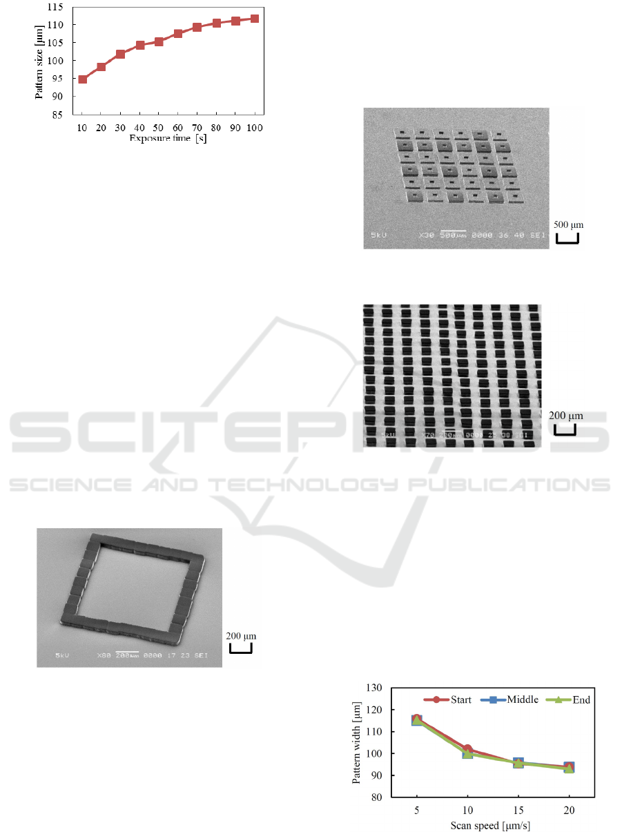
Figure 7: Pattern size controllability by adjusting the
exposure time.
fabricated by lighting only the fiber elements at outer
periphery. It has a 800-μm square hollow chamber
surrounded by a 100-μm wide outline fence. Figure 9
shows a cell array fabricated by lighting LEDs
corresponding to 3×3 fiber elements except the center,
and repeating exposures and step movements.
Repeated 300-μm square cell patterns with 100-μm
square hollows were regularly printed.
In Figure 8 and 9, concave chamber and cells were
directly fabricated. However, it is also possible to
print convex resist patterns at first, and replicate the
patterns to PDMS using soft lithography (Wang et al.,
2008). Figure 10 shows an example of convex resist
pattern array. Square dot patterns with a size and a
pitch of 100 and 200 μm were regularly printed in a
wide area. Cell arrays would be fabricated by
replicating them to PDMS using soft lithography.
Thus, it was demonstrated that various chamber
and cell array patterns were easily fabricated by the
new exposure system without using reticles.
Figure 8: Chamber pattern with 800-μm square chamber
and 100-μm wide fence.
3.2 Scan Exposure
It was demonstrated that arbitrary patterns were
printable by assigning LED lighting maps. However,
curved or oblique patterns were not printable by the
direct exposure using the squared fiber matrix. For
this reason, scan exposure using automatic stage
control was investigated next. Exposure light spots
with a 100-μm square shape were relatively moved in
X and Y directions by scanning the wafer stage. Scan
speeds were changed between 5 μm/s and 20 μm/s.
Figure 11 shows the relationship between the scan
speed and measured pattern width. Pattern width was
controllable between 93 and 115 μm by changing the
scan speed.
Figure 9: Dispersively arrayed 300-μm square patterns with
100-μm square hollow cells.
Figure 10: Arrayed 100-μm square pillars. If patterns were
replicated to PDMS using soft lithography, a cell array
would be obtained.
Next, a flow-path mold of a micro-mixer with a
width of 100 μm was fabricated by scanning a light
spot from one LED at a scan speed of 10 μm/s.
However, at the inlets and outlet of the mixer, all the
LEDs were lit, and 1-mm square patterns were printed
without scanning the stages. Fabricated flow path
pattern is shown in Figure 12. Patterns were
successfully delineated in 6×12 mm
2
area.
Pattern widths were measured at 15 points, as
shown in Figure 13. Figure 14 shows the results.
Figure 11: Pattern width control by adjusting the scan
speed.
BIODEVICES 2016 - 9th International Conference on Biomedical Electronics and Devices
206
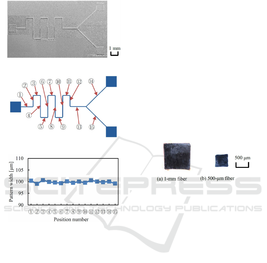
Figure 12: Micro-fluidic device pattern.
Figure 13: Points selected for measuring pattern widths.
Figure 14: Width homogeneity of fabricated micro-fluidic
device patterns.
Pattern widths of vertical parts and horizontal parts
were almost uniform. In addition, widths of 45°
oblique patterns became almost the same as those of
the vertical and horizontal patterns. Deviation of line
widths for all the measurement points was as small as
less than 1μm.
4 EXTENDABILITY
It was demonstrated that various biodevice patterns
were easily fabricated using the new system.
However, the minimum pattern size was decided by
the fiber size, and it was approximately 100 μm. In
some cases, patterns with smaller sizes are required.
For this reason, it was investigated whether finer
squared fibers were obtained or not. Figure 15 shows
a cross section of 500-μm square fiber. The fiber was
fabricated by deforming the end of a circular fiber
with a diameter of 500 μm. It was verified that the
profile and corner roundness were almost the same as
those of 1-mm fiber. Accordingly, it is probably
possible to reduce the minimum pattern size at least
to 50 μm. If the element fiber size is reduced in a half,
and LED light rays are efficiently collected in the
fiber, the intensity of light spot on a wafer is increased
by a factor of 4, and the exposure time is reduced to
1/4.
On the other hand, if the new system is applied to
fabrication processes of biodevices using etching, and
resist patterns are used as etching masks, highly
sensitive thin positive resist is applicable. In such
cases, exposure time becomes considerably short. For
example, even using 1-mm square fiber-matrix,
patterns were printable within 4 s using 1-μm thick
THMR iP-3300PM (Tokyo Ohka Kogyo). The new
exposure system is very flexible and has a wide
extendability.
Figure 15: Half-size squared optical fiber with a cross
section profile similar to that of current size fiber.
5 CONCLUSIONS
Applicability of the newly developed low-cost
maskless exposure system to the fabrication of
biodevices was investigated. In the new system,
LEDs were used as original exposure sources, and a
squared optical fiber matrix was used as a component
combining a secondary light source and a reticle with
bright and dark parts. It was demonstrated that
various chamber or cell arrays were directly
fabricated using 30-μm thick negative resist and LED
lighting control. In addition, combining with the
scanning exposure, a flow path pattern applicable to
a replica mold for soft lithography using PDMS was
fabricated. It was verified that the new exposure
system was prospective for the use of biodevice
fabrication. If optical fibers with a smaller diameter
are used, and the matrix size is enlarged in future,
convenience and applicability will be extended
further. The minimum element pattern size, pattern
size accuracy and repeatability, and other
performances of the exposure system should be
investigated further more hereafter.
New Maskless Lithography System for Fabricating Biodevices using Light-Emitting Diodes and Squared Optical Fibers
207

ACKNOWLEDGEMENTS
This work was partially supported by Grant-in-Aid
from J I Engineering, and Research institute for
Science and Technology of Tokyo Denki University,
Grant Number QT15-03.
REFERENCES
Arnandis, C. T., Morais, S., Tortajada, G. L. A., Puchades,
R., Maquieira, A., Berganza, J., and Olabarria, G., 2012.
Detection of food-borne pathogens with DNA arrays on
disk. Talanta, 101, pp. 405-412.
Boero, C., Casulli, A. M., Olivo, J., Foglia, L., Orso, E.,
Mazza, M., Carrara, S., and Micheli, D. G., 2014.
Design, development, and validation of an in-situ
biosensor array for metabolite monitoring of cell
cultures. Biosensors and Bioelectronics, 61, pp. 251-
259.
Bianchi, E., Molteni, R., Pardi, R., and Dubini, G., 2013.
Microfluidics for in vitro biomimetic shear stress-
dependent leukocyte adhesion assays. Journal of
Biomechanics, 46, pp. 276-283.
Choi, H. J., Ogunniyi, O, A., Du, M., Du, M., Kretschmann,
M., Eberhardt, J., and Love, C, J., 2010. Development
and Optimization of a Process for Automated Recovery
of Single Cells Identified by Microengraving.
Biotechnology progress, 26, pp. 888-895.
Gach, C. P., Attayek, J. P., Whittlesey, L. R., Yeh, J. J., and
Allbritton, L. N., 2014. Micropallet arrays for the
capture, isolation and culture of circulating tumor cells
from whole blood of mice engrafted with primary
human pancreatic adenocarcinoma. Biosensors and
Bioelectronics, 54, pp. 476-483.
Ilyas, A., Asghar, W., Kim, Y., and Iqbal, M. S., 2014.
Parallel recognition of cancer cells using an addressable
array of solid-state micropores. Biosensors and
Bioelectronics, 62, pp. 343-349.
Kim, J., Hilton, P. J., Yang, K., Pei, R., Stojanovic, M., and
Lin, Q., 2013. Nucleic acid isolation and enrichment on
a microchip. Sensors and Actuators, A 195, pp. 183-
190.
Lei, F. K., Wu, M., Hsu, C., and Chen, Y., 2014. Real-time
and non-invasive impedimetric monitoring of cell
proliferation and chemosensitivity in a perfusion 3D
cell culture microfluidic chip. Biosensors and
Bioelectronics, 51, pp. 16-21.
Li, S., Floriano, N. P., Christodoulides, N., Fozdar, Y. D.,
Shao, D., Ali, F. M., Dharshan, P., Mohanty, S., Neikirk,
D., McDevitt, T. J., and Chen, S., 2005. Disposable
polydimethylsiloxane/silicon hybrid chips for protein
detection. Biosensors and Bioelectronics, 21, pp. 574-
580.
Lyu, S., Chen, W., and Hsieh, W., 2014. Measuring
transport properties of cell membranes by a PDMS
microfluidic device with controllability over changing
rate of extracellular solution. Sensors and Actuators, B
197, pp. 28-34.
Malainou, A., Petrou, S. P., Kakabakos, E. S., Gogolides,
E., and Tserepi, A., 2012. Creating highly dense and
uniform protein and DNA microarrays through
photolithography and plasma modification of glass
substrates. Biosensors and Bioelectronics, 34, pp. 273-
281.
Moraes, C., Wang, G., Sun, Y., and Simmons, A. C., 2010.
A microfabricated platform for high-throughput
unconfined compression of micropatterned biomaterial
arrays. Biomaterials, 31, pp. 577-584.
Negrete, D. O., and Cerrina, F., 2008. Step-and-scan
maskless lithography for ultra large scale DNA chips.
Microelectronic Engineering, 85, pp. 834-837.
Schmidt, R., Cook, A. E., Kastelic, D., Taussig, J. M., and
Stoevesandt, O., 2013. Optimised ‘on demand’ protein
arraying from DNA by cell free expression with the
‘DNA to Protein Array’ (DAPA) technology. Journal
of protemics, 88, pp. 141-148.
Tanii, T., Hosaka, T., Miyake, T., Zhang, G., Zako, T.,
Funatsua, T., and Ohdomari, I., 2004. Preferential
immobilization of biomolecules on silicon
microstructure array by means of electron beam
lithography on organosilane self-assembled monolayer
resist. Applied Surface Science, 234, pp. 102-106.
Wang, T. C., and Hu, C. Y., 2010. Mixing of Liquids Using
Obstacles in Y-Type Microchannels. Tamkang Journal
of Science and Engineering, 13, No. 4, pp. 385-394.
Wang, H., Bao, N., and Lu, C., 2008. A microfluidic cell
array with individually addressable culture chambers.
Biosensors and Bioelectronics, 24, pp. 613-617.
BIODEVICES 2016 - 9th International Conference on Biomedical Electronics and Devices
208
