Improvement of Perovskite Solar Cells Photovoltaic Performance by
Localized Surface Plasmon Effect of Silver-alumina Core-shell
Nanoparticles
Marziyeh Yaghubinia
1
, Majid Ebnali
2
, Mahmoud Zendehdel
3
and Mohammadreza Yaghoubinia
4
1
Department of Electronic Engineering, Islamic Azad University of Najaf Abad, Isfahan, Iran
2
Department of Electronic Engineering, Shahrekord University, Shahrekord, Iran
3
Research and Development Section, Kimia Solar Company, Isfahan, Iran
4
Department of Electronic Engineering, Islamic Azad University of Khorasgan, Isfahan, Iran
Keywords: Perovskite, Solar Cell, Plasmon Effect, Core-shell.
Abstract: Perovskite solar cells are new generation of nanostructure-based solar devices that could reach to highest
efficiency records between third generation solar cells. In present project, for the first time, enhancement of
the photovoltaic performance of planner perovskite solar cells is achieved by using localized surface
Plasmon (LSP) effect of silver-alumina core-shell nanoparticles as a dopant in the perovskite layer.
Photovoltaic performances of the devices are evaluated by FE-SEM, IV measurement, cyclic voltammetry,
UV-Vis spectroscopy and electrochemical impedance spectroscopy. The results show significant increase of
the overall efficiency and short-circuit current density of the devices by using LSP effect of Ag-Al2O3
nanoparticles.
1 INTRODUCTION
Solid-state thin film solar cells represent a promising
technology to harvest and convert solar energy to
electricity efficiently and cost-effectively (Sargent,
2012). There exists a plethora of technologies,
ranging from thin film absorber layers of binary and
tertiary semiconductor compounds (Katagiri et al.,
2009), to demixed polymer blends, where nano to
mesostructure is essential to efficiently ionize
excitons (the primary excited state following light
absorption) and extract charge. Very recently,
organometal halide perovskites have been employed
as the absorber layer in hybrid solar cells, exhibiting
exceptionally low loss photovoltaic operation, as
well as a simple solution based synthetic route from
abundant sources (C, N, Pb and halogen). Miyasaka
and coworkers first reported a 3.8% efficient
CH3NH3PbI3 “perovskite sensitized” solar cell
(PSC), employing a liquid electrolyte in a
conventional dye-sensitized solar cell (DSC)
architecture (Kojima et al., 2009). By replacing the
liquid electrolyte with a solid organic hole conductor
spiro-OMeTAD (2,2’,7,7’-tetrakis (N,N-di-p-
methoxyphenylamine)-9,9′-spirobifluorene), Park
and coworkers and ourselves achieved between 8 to
9.7% efficiency based on perovskite sensitized
mesoporous TiO2 devices (Kim et al., 2012), and
Etgar and coworkers demonstrated operating
mesoporous TiO2-perovskite solar cells without any
additional hole-transporter (redox couple) (Etgar et
al., 2012).
Since the inorganic-organic hybrid perovskite
solar cell was first reported in 2009 (Kojima et al.,
2009), its power conversion efficiency (PCE) was
rapidly improved to as high as 19.3% by now, and
could ultimately boost efficiencies to 25% as high as
that of single-crystal silicon cell (Service, 2014). To
further improve the efficiency, it is necessary to
extend light absorption spectrum to harvest more
energy in thin film solar cells, without increasing the
thickness and the complexity of the devices (Ogomi
et al., 2014). Although the absorption coefficient of
hybrid perovskite at 550 nm is around 1.5×104 cm-
1, as strong as organic materials, the absorption is
drop-down around band edge (Kazim et al., 2014).
Therefore, it should be promising to greatly enhance
the light absorption of hybrid perovskite around the
band edge.
272
Yaghubinia, M., Ebnali, M., Zendehdel, M. and Yaghoubinia, M.
Improvement of Perovskite Solar Cells Photovoltaic Performance by Localized Surface Plasmon Effect of Silver-alumina Core-shell Nanoparticles.
DOI: 10.5220/0005792802700272
In Proceedings of the 4th International Conference on Photonics, Optics and Laser Technology (PHOTOPTICS 2016), pages 272-274
ISBN: 978-989-758-174-8
Copyright
c
2016 by SCITEPRESS – Science and Technology Publications, Lda. All rights reserved

To boost the solar cells’ light absorption, one of
the promising methods is to apply noble metal
nanoparticles, on which localized surface plasmon
(LSP) resonance can be excited under the light
illumination. The confined electromagnetic energy
based on LSP resonance could greatly improve the
light absorption of active medium surrounding the
nanoparticles (NPs) (Chen et al., 2013). The light
absorption enhancement and efficiency
improvement of different kinds of solar cells,
including thin film Si solar cells, dye-sensitized
solar cells (DSCs) (Qi et al., 2011), and organic
photovoltaics (OPVs) (Lu et al., 2013), had been
reported recently.
In present project, for the first time, localized
surface Plasmon effect of core-shell structure of
silver-alumina nanoparticles on photovoltaic
parameters of perovskite solar cells with planner
architecture based on Pb(CH
3
NH
3
)I
3
sensitizers, is
investigated. Performance of the devices are
evaluated by I-V measurement, cyclic voltammetry,
UV-Vis spectroscopy and electrochemical
impedance spectroscopy (EIS) and compared to
perovskite solar devices without LSP effect.
2 MATERIALS AND METHODS
The patterned substrates FTO were cleaned in an
ultrasonic bath, using detergent with de-ionized
water, acetone and isopropanol (10 minutes for each
step). Patterning of the TiO2 layer about 50nm was
achieved by using the dip coating method (multi-
purpose dip coating machine of Kimia Solar Co,
model: mpDCTT-1200). DektakVeeco 150
profilometer was used for measurement the
thickness of the blocking layer.
The lead iodide solution (PbI2 in N,N-
dimethylformamide, 460 mg ml-1) was made. Then
10 ppm silver-Alumina nanoparticles added in the
solution of PbI2, finally spin coated with 6000 r.p.m
for 10 sec then dried at 70 °C for 1 hr.
CH3NH3PbI3 crystallization was achieved by
dipping the PbI2 layer in a methylammonium iodide
solution (CH3NH3I in anhydrous 2-propanol 10 mg
ml-1) for 2 minutes then immediately washed with
2-propanol by spin coating method at 6000 r.p.m for
10 sec and dried at 70 °C for 30 min.
The hole-transporting layers was deposited by
spin-coating a 75 mg ml-1 solution of 2,20,7,70-
tetrakis-(N,N-dip-methoxyphenylamine)9,9’-
spirobifluorene (Spiro-OMeTAD), doped with 8 μl
of tert-butylpyridine and 11 μl of Lithium
Bis(Trifluoromethanesulfonyl)Imide (Li-TFSI)
solution (520mg in 1 ml of acetonitrile), was spin
coated by 2000 rpm for 45 second and thickness was
around 250nm (the thickness of all samples checked
by DektakVeeco 150 profilometer).
Samples were introduced into a high vacuum
chamber (10-6 mbar) to thermally evaporate Au
back contacts (thickness 80 nm).
Masked devices were tested under a solar
simulator (Kimia Solar sun simulator model: SSTT-
1100) at AM1.5G and 100 mW cm-2 illumination
conditions calibrated with a certified reference Si
Cell (RERASolutions RR-1002). Incident power
was measured with a Skye SKS 1110 sensor. The
absorbance was measured with a BLACK-Comet
UV-VIS Spectrometer. The morphology and grain
size of the PbI2, perovskite and HTM layers
obtained with Scanning Electron Microscopy (FE-
SEM). Electrochemical analysis was measured with
Autolab Instrument.
3 RESULTS
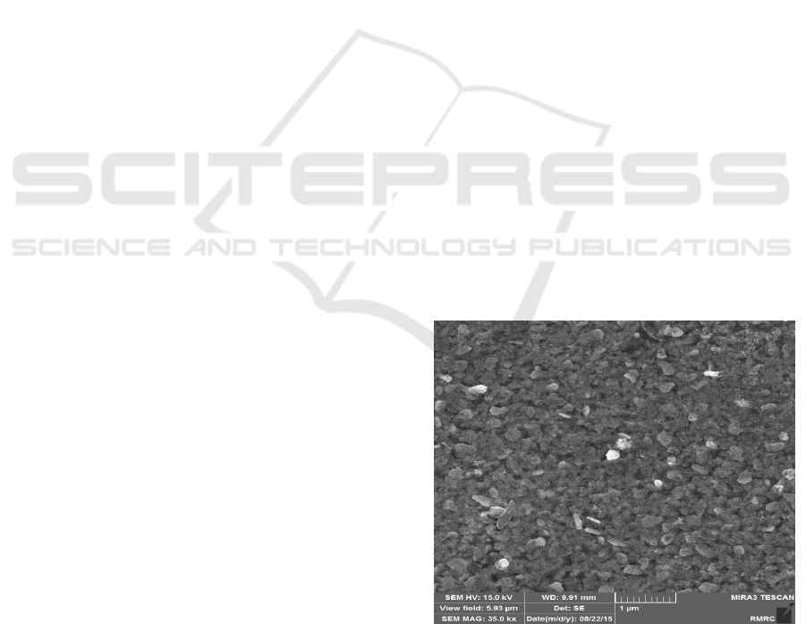
The Scanning electron microscopic images and UV-
Vis measurement of the perovskite layers shows in
the figures 1 and 2, respectively. The SEM shows
that the perovskite layer is quite homogenous and
the size of the crystal was around 100 nm. From the
UV-VIS measurement it observed with adding the
Silver-alumina nanoparticle as a dopant in the
perovskite the absorbance increased which is relate
to the LSP effect as we expect from the theoretical
investigation.
Figure 1: FE-SEM image of perovskite layer containing
Ag-Al
2
O
3
nanoparticles.
Improvement of Perovskite Solar Cells Photovoltaic Performance by Localized Surface Plasmon Effect of Silver-alumina Core-shell
Nanoparticles
273

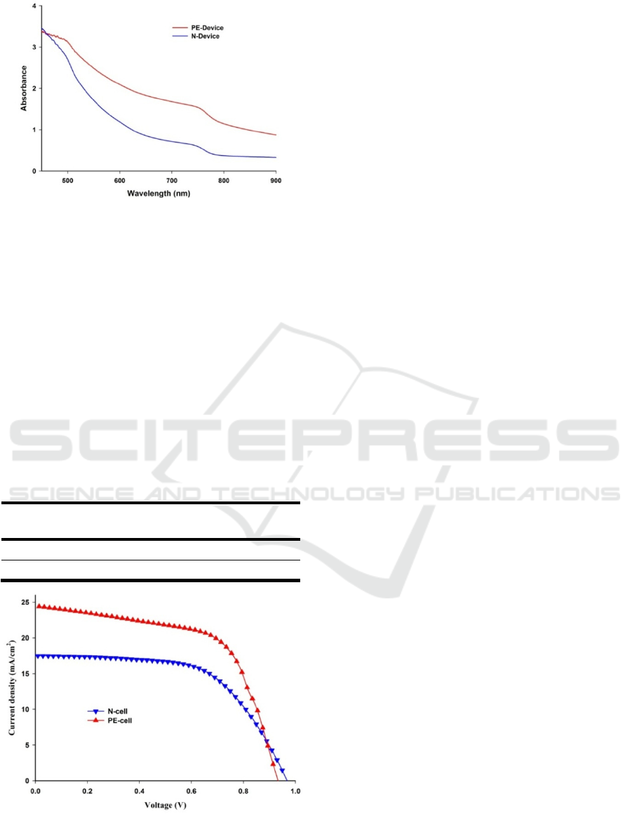
Figure 2: UV-Vis absorbance spectra of perovskite layers.
The results of I-V measurement analysis spectra
and the photovoltaic parameters of the devices under
AM1.5G illumination are present in figure 3 and
table 1, respectively. By insertion of Ag-Al
2
O
3
nanoparticles in the perovskite layer, short circuit
current density (J
sc
) of the device is significantly
enhanced which led to increase of the overall
efficiency from 10% to 13.9%. Furthermore, the
other photovoltaic parameters have not been varied
by insertion of Ag-Al
2
O
3
nanoparticles. These
results proof our proposal for enhancement of the
perovskite absorbance by positive LSP effect of
core-shell nanoparticles.
Table 1: Photovoltaic parameters of perovskite solar cells
with and without LSP effect.
Sample V
oc
(v)
J
sc
(mA/cm
2
)
FF PCE (%)
PE-cell 0.934 24.5 0.61 13.9
N-cell 0.969 17.5 0.59 10.0
Figure 3: I-V measurement plots of the perovskite solar
cell devices with LSP effect (PE-cell) and normal device
without LSP effect (N-cell).
4 CONCLUSIONS
In this project, for the first time, effect of localized
surface Plasmon on the perovskite solar device with
planner structure is successfully investigated.
Photovoltaic performance of the devices shows
enhancement of Jsc and overall efficiency by using
LSP effect of silver-alumian core-shell structure
nanoparticles inside the perovskite layer as dopant.
ACKNOWLEDGEMENTS
This study was financially supported by Kimia Solar
Co, Isfahan, Iran and Islamic Azad University of
Najaf Abad, Isfahan, Iran.
REFERENCES
Sargent, E. H. Nat Photonics 2012, 6, (3), 133-135.
Katagiri, H.; Jimbo, K.; Maw, W. S.; Oishi, K.; Yamazaki,
M.; Araki, H.; Takeuchi, A. Thin Solid Films 2009,
517, (7), 2455-2460.
Kojima, A.; Teshima, K.; Shirai, Y.; Miyasaka, T. J Am
Chem Soc 2009, 131, (17), 6050–6051.
Kim, H. S.; Lee, C. R.; Im, J. H.; Lee, K. B.; Moehl, T.;
Marchioro, A.; Moon, S. J.; Humphry-Baker, R.;
Yum, J. H.; Moser, J. E.; Grätzel, M.; Park, N. G. Sci
Rep-Uk 2012, 2.
Etgar, L.; Gao, P.; Xue, Z. S.; Peng, Q.; Chandiran, A. K.;
Liu, B.; Nazeeruddin, M. K.; Gratzel, M. J Am Chem
Soc 2012, 134, (42), 17396-17399.
R. F. Service, Science, 2014, 344, 458.
Y. Ogomi, A. Morita, S. Tsukamoto, T. Saitho, N.
Fujikawa, Q. Shen, T. Toyoda, K. Yoshino, S. S.
Pandy, T. Ma and S. Hayase, J. Phy. Chem. Lett.,
2014, 5, 1004-1011.
S. Kazim, M. K. Nazeeruddin, M. Graätzel and S. Ahmad,
Angew. Chem., Int. Ed., 2014, 53, 2812-2824.
H. Chen, L. Shao, Q. Li and J. Wang, Chem. Soc. Rev.,
2013, 42, 2679–2724.
J. Qi, X. Dang, P. T. Hammond and A. M. Belcher, ACS
Nano, 2011, 5, 7108–7116.
L. Lu, Z. Luo, X. Tao and L. P. Yu, Nano Lett., 2013, 13,
59−64.
PHOTOPTICS 2016 - 4th International Conference on Photonics, Optics and Laser Technology
274
