Wireless Energy and Data Transmission ASIC for Blood Pressure
Measurement in an Aneurysm Implant
Rajeev Ranjan, Bibin John, Dipal Gosh, Soumil Kumar, Lait Abu Saleh, Dietmar Schroeder
and Wolfgang H. Krautschneider
Institute of Nano and Medical Electronics, Hamburg University of Technology,
Eissendorfer Str. 38, 21073, Hamburg, Germany
Keywords:
Aneurysm Implant, Blood Pressure Measurement, Stent Graft, Forward Error Correction.
Abstract:
Aneurysm implant requires multiple pressure sensors integrated into the stent graft for recording pressure
profile inside an aneurysm sac. This paper details the design of an ASIC which receives power wirelessly
using inductive coupling, fetches pressure data from a seperate chip and transmits data wirelessly. Besides,
the ASIC extends the functionality of the external pressure measurement chip to support up to four pressure
sensors by using an analog multiplexer. Error detection and forward error correction are implemented to
improve data integrity for wireless data transmission. The design has been implemented and tested in 350 nm
CMOS technology.
1 INTRODUCTION
Aneurysm is the dilation of the artery due to weak-
ening of the arterial wall, which occurs in 5-10% of
older men and in 1-2% of older women (Silverstein
et al., 2005). Endovascular aneurysm repair (EVAR)
using an implantable stent graft is a minimally inva-
sive method for abdominal aortic aneurysm treatment.
The complication after an EVAR stent insertion is the
endoleakage, which is the leakage of blood around the
stent graft (Drury et al., 2005).
Endoleak will add trauma to the weakened arte-
rial walls of the aneurysm, which can cause further
enlargement or even risk of rupture. Most of the en-
doleaks are discovered within 30 days of operation
but sometimes they do not manifest themselves until
up to 7 years after surgery (Corriere et al., 2004). Up
to 40% of patients underwent EVAR suffer from en-
doleak. The long time window of the endoleaks and
high probability of its occurrence necessitates moni-
toring of the patients periodically for many years.
Currently, contrast-enhanced computed tomogra-
phy (CT) or ultrasound is used to detect endoleaks
after EVAR operation. This method does not allow
real-time measurement of intrasac aneurysm pressure
level, and it require patients to visit hospital periodi-
cally. These shortcomings can be reduced by using a
new approach. This approach integrates pressure sen-
sors into the commercially available stent graft used
for EVAR repair. Pressure sensors together with other
electronic components form an implant. This implant
must transmit pressure data wirelessly and it should
be powered wirelessly (Koops et al., 2013).
2 IMPLANT REQUIREMENTS
The implant consists of an array of pressure sensors
evenly distributed and mounted on the outer surface of
the stent graft for assessing pressure distribution in the
aneurysm sac with high spatial resolution. The pres-
sure data is sent wirelessly and the implant is pow-
ered wirelessly by inductive coupling. The implant
together with stent graft must be able to fit into a com-
mercially available 24F applicator stent delivery sys-
tem (Spink et al., 2015).
The implant is located inside the body of the pa-
tient where the distance between the wireless power
sender and the implant is greater than 10 cm. So
the sensors and electronic components in the implant
must work at very low-power. The implant should
survive mechanical stresses generated due to the stent
insertion procedure during EVAR operation. For a
good mechanical performance, it is advised to have
few electronic components integrated on a flexible
PCB substrate to be mounted on the stent (Bradford
256
Ranjan, R., John, B., Gosh, D., Kumar, S., Saleh, L., Schroeder, D. and Krautschneider, W.
Wireless Energy and Data Transmission ASIC for Blood Pressure Measurement in an Aneurysm Implant.
DOI: 10.5220/0005815002560262
In Proceedings of the 9th International Joint Conference on Biomedical Engineering Systems and Technologies (BIOSTEC 2016) - Volume 1: BIODEVICES, pages 256-262
ISBN: 978-989-758-170-0
Copyright
c
2016 by SCITEPRESS – Science and Technology Publications, Lda. All rights reserved

et al., 2010).
This ASIC design aims to minimize the number of
electronic components in the implant to be mounted
on the stent. This is realized by integrating wire-
less power reception and wireless data transmission
on a single die. Furthermore, instead of state of
the art resistive sensors, a capacitive pressure sen-
sor is used in order to reduce power consumption.
An external(off-chip,on stent) Capacitance to Digital
Converter (CDC) chip, ZSSC3123 (ZMDI, 2015), is
used to drive the capacitive pressure sensor. The die
of ZSSC3122 is used to fit into the dimension of im-
plant. The CDC can support only one pressure sensor,
but the ASIC extends this functionality to support up
to four sensors using an analog multiplexer designed
on chip. Further the CDC can be designed on-chip for
independent solution.
3 ARCHITECTURE AND DESIGN
Wireless Power Reception
Wireless Data Transmssion
LDO
Recti
er
Reference
Level shifter
120V
NMOS
Charge Pump
SPI communication
Analog MUX
Channel control
Error Correction
CRC checksum
Digital module
Capacitance to
Digital Converter
ZSSC3123
ASIC
Collision avoidance
Clock extraction
pressure
sensor
Figure 1: Chip architecture.
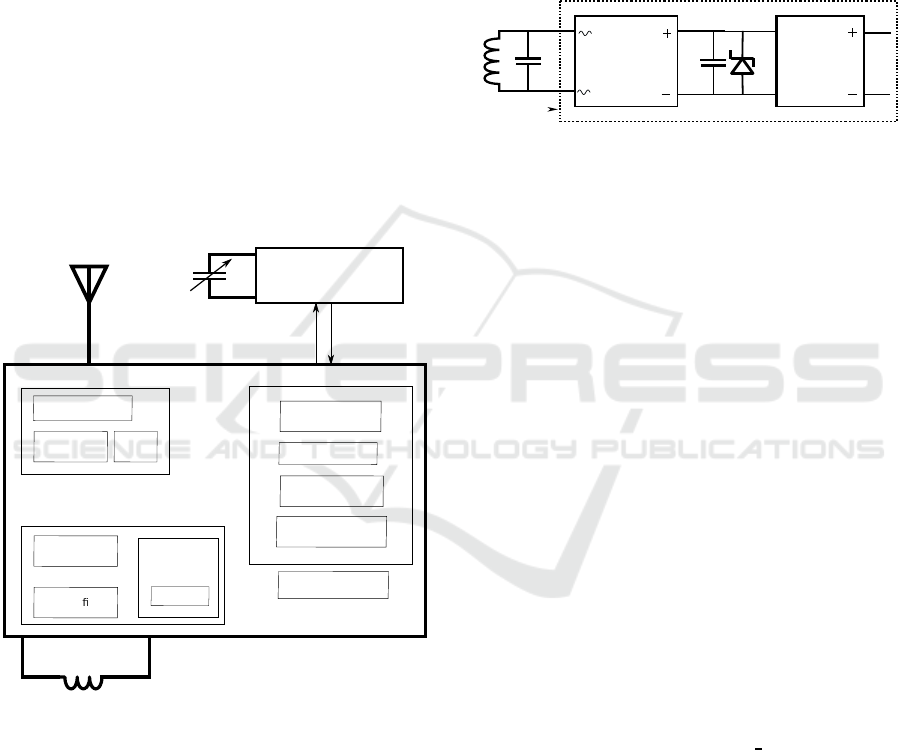
A block diagram of the ASIC is shown in figure 1. It
consists of three main modules: wireless power recep-
tion, wireless data transmission and the digital mod-
ule. The wireless power reception module receives
energy through inductivecoupling to power the whole
implant. It has on-chip rectifier and Low Dropout
Regulator(LDO) which converts sine signal into reg-
ulated 3.3V supply for full chip. An on-chip digi-
tal module fetches the pressure sensor data from the
CDC chip and sends it to the wireless data transmis-
sion module. The wireless data transmission module
transmits the pressure data to the outside world.
3.1 Wireless Power Reception
The wireless power receiving module provides a reg-
ulated constant output voltage of 3.3 V from the wire-
less energy received from the resonant LC circuit.
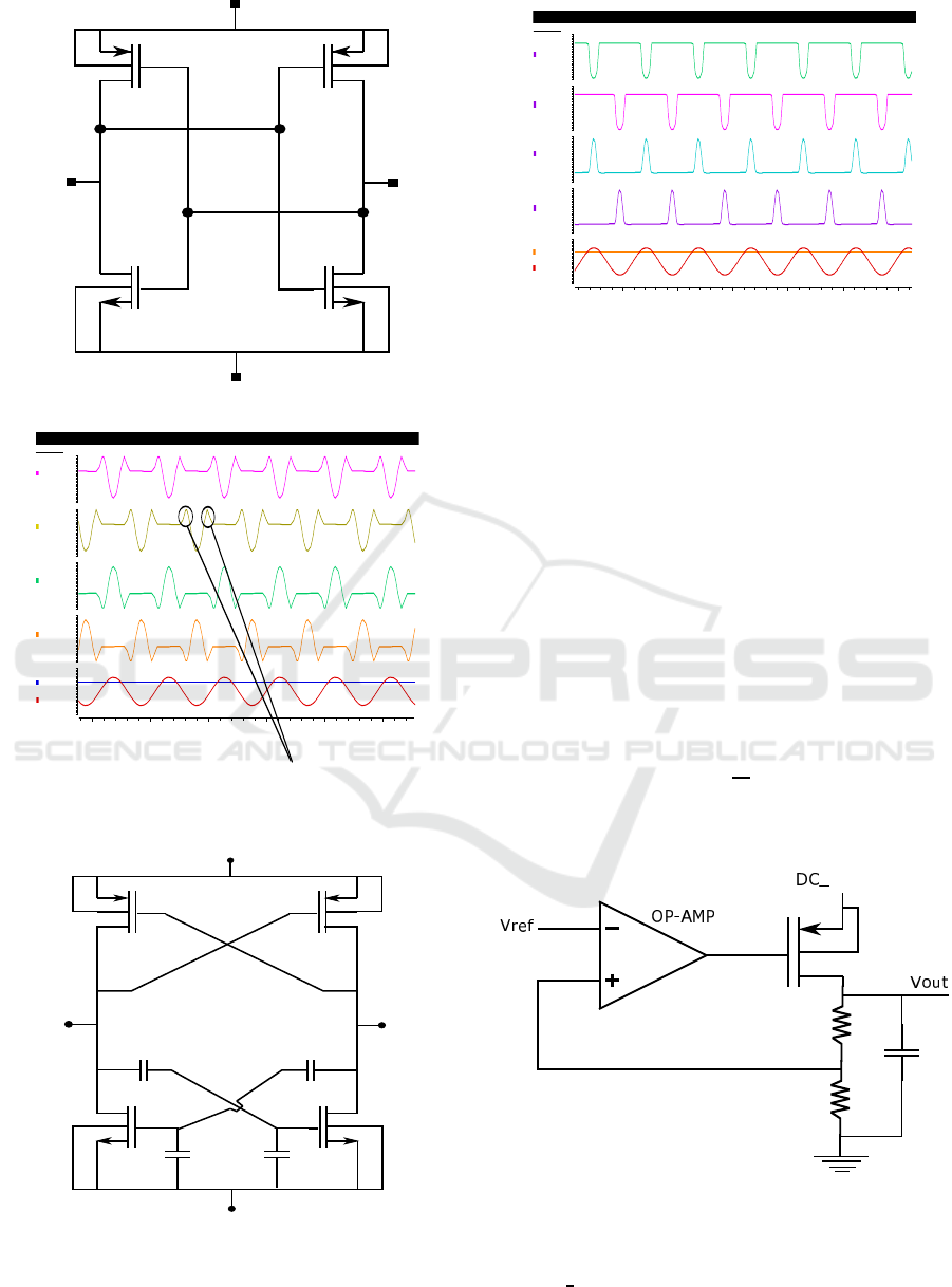
The block diagram of this module is shown in fig-
ure 2. An off-chip resonance circuit consisting of
L and C1 receives wireless power through inductive
coupling. The output of the resonace circuit is con-
nected to the chip’s input as depicted in figure 2.
Full Wave Rectifier
3.3V
GND
L
C1
C2
LDO
ASIC
Figure 2: Wireless power reception module.
The Capacitor C2 is used for energy storage and
the zener diode for overvoltage protection.LDO has
been used to provide a stable DC supply voltage of
3.3V and power of 1mW to the rest of the modules in
the ASIC.
3.1.1 Rectifier
The rectifier is the first front end block of the ASIC
which converts the wirelessly received AC signal into
pulsating DC signal. There are fundamentally two
types of rectifiers, half wave and full wave rectifier.
In this ASIC a full wave rectifier has been designed
because of it’s high efficiency. The conventional full
wave rectifier has the fundamental problem of thresh-
old drop at the output. The cross coupled structure
has been used for this threshold cancellation (Kotani
et al., 2009) (Kotani and Ito, 2007) as shown in fig-
ure 3. In spite of the threshold voltage (Vth) can-
cellation, the rectifier suffers from uncontrolled bias-
ing of the mosfet rectifier diodes (Kotani et al., 2009)
which leads to high leakage current as shown in fig-
ure 4. During the turning on of MP2 and turning
off of MN2, there is an intermediate state when both
MP2 and MN2 conduct as seen in figures 3 and 4.
This causes current flow from DC
output to ground
as leakage current. This paper proposes a modified
design which uses a cross coupled capacitive divider-
based static biasing of the NMOS diodes (MN1 and
MN2) to reduce the mentioned leakage current and
obtain high efficiency.
In the conventional design shown in figure 3,
for the positive half cycle MP2 and MN1 conduct
whereas for the negative half cycle MP1 and MN2
conduct (Kotani and Ito, 2007) (Kotani et al., 2009).
During the time when the sine input signal changes
from low to high or high to low, there is a leakage
Wireless Energy and Data Transmission ASIC for Blood Pressure Measurement in an Aneurysm Implant
257

MP2 MP1
MN2
MN1
Sin+
Sin-
DC_output
Ground
Figure 3: Conventional rectifier with Vth cancellation.
Name
I (mA)
0.0
-20.0
10.0
-10.0
I (mA)
-20.0
-10.0
0.0
10.0
-10.0
I (mA)
20.0
0.0
10.0
I (mA)
-10.0
0.0
10.0
20.0
V (V)
-7.5
-2.5
2.5
7.5
2.8255
time (ms)
2.82425 2.8245 2.82475 2.825 2.82525
Transient Response
DC output
Input Sine
MP1/D
MP2/D
MN2/D
MN1/D
Leakage current
Figure 4: Conventional rectifier output.
C1C1
C2
C2
MN1
MN2
MP1MP2
Sin-
GND
DC_output
Sin+
Figure 5: Rectifier circuit of the ASIC.
current which is labelled as ”Leakage current” in the
figure 4. In the proposed rectifier design shown in
I (mA)
-2.0
-1.5
-1.0
-.5
0.0
.5
-2.0
-1.5
-1.0
-.5
0.0
.5
I (mA)I (mA)
-2.5
0.0
2.5
5.0
7.5
10
I (mA)
-2.5
0.0
2.5
5.0
7.5
10
7.5
-7.5
-2.5
2.5
V (V)
Name
time (ms)
2.909 2.90925 2.9095 2.90975 2.91 2.91025
Transient Response
Input Sine
DC output
MP1/D
MP2/D
MN2/D
MN1/D
Figure 6: Rectifier output of the ASIC.
figure 5, a static biasing has been done for MN1 and
MN2 which allows MN1 and MN2 to conduct only
for the time when MP2 and MP1 conducts, provid-
ing an extremely low leakage shown in figure 6 and
high efficiency of 74%. The capacitive divider C1
and C2 divides the voltage level between Sin+/Sin-
and ground. The ratio of C1 and C2 is selected so
that the voltage at the gate reaches Vth only when the
input sinus voltage is above DC output voltage.
3.1.2 Low Dropout Regulator
The conventional low dropout regulator (Milliken
et al., 2007) has been designed in this ASIC with re-
sistive feedback as shown in figure 7.
Vout = (1 +
R1
R2
) ×Vref
where Vref is the referance voltage generated by
the on-chip bandgap.
R1
R2
C
P1
output
Figure 7: Low Dropout Regulator.
The regulation of the output voltage starts when
the rectifier input voltage is above 9V (peak to peak)
and DC
output above 3.3V. Figure 8 shows the com-
parison between simulated and measured output volt-
age of the LDO for different rectifier input voltages.
BIODEVICES 2016 - 9th International Conference on Biomedical Electronics and Devices
258

4 5 6 7 8 9 10 11 12 13
1
1.5
2
2.5
3
3.5
Measured Output Voltage
Simulated Output Voltage
LDO output voltage
fi input
Figure 8: Measured and simulated output voltage of the
wireless power receiving block.
3.2 Digital Module
ready=1
Initialisation
IDLE
NEW_CHANNEL
READ_ZMDI
PACKAGE_DATA
Error Correction
Error Detection
DATA_OUTPUT
delay,Taddr
Figure 9: Finite state machine.
The clock extraction block (figure 1) provides clock
input for the digital module. The frequency of this
clock is dependent on the frequency of the external
(outside body) wireless power sender. An internal
clock divider in the digital module reduces this fre-
quency down to 3 kHz. This has been done to reduce
the power consumed by the digital module.
The Commercially available CDC supports only
one pressure sensor. The on-chip analog MUX mul-
tiplexes the excitation signal generated by the CDC
to one of the four pressure sensors based on the input
channel settings of the digital module.
The digital module is implemented using the Fi-
nite State Machine (FSM) as shown in figure 9. This
module communicates with the CDC using an SPI in-
terface. The ’Ready’ signal is an interrupt from the
CDC signalling new pressure data. After reception
of 14 bit pressure value, a new channel is selected to
switch CDC excitation signal to a new pressure sen-
sor. Later, pressure data is fetched from the CDC.
An error in the received data at the external (out-
side body) reader hardware is identified using a Cycle
Redundancy Checksum (CRC). The polynomial used
for this CRC is p(x) = x
5
+ x
2
+ 1.
In a traditional approach, when corrupt data is
identified by the external reader hardware, it either
discards the whole data packet or signals the implant
to resend the data. Resending data approach costs fur-
ther area for wireless data reception (envelope detec-
tor, amplifier, comparator etc...) on the chip and extra
energy for data re-transmission. This can be avoided
by using Forward Error Correction (FEC).
Reed-Solomon error correction is implemented in
this chip (Tej and Jhansi Rani, 2013). By adding 16
bits of Reed-Solomon code to the 20-bits of data, it
is possible to correct up to 8-bits of data. The pa-
rameters of the Reed-Solomon code are m=4, n=9,
k=5 and t=2. The generator polynomial g(x) = x
4
+
13x
3
+ 12x
2
+ 8x+ 7 is based on the primitive poly-
nomial p(x) = x
4
+ x + 1.
START
1111
sure
value, channel (20bits)
addr0, addr1, C0, C1....C12,
C13, ch0,ch1,addr0,addr1
Error Correction
(16 bits)
EC0,EC1,....,EC15
CRC-5
(5 bits)
crc0,..crc4
STOP
(1 bit)
1
Figure 10: Data packet output of the digital module.
The data packet is shown in figure 10. The data
containing address of the chip, pressure value and the
channel number counts to 18 bits. But two address
bits are added again to it make it 20 bits (k=5) be-
cause error correction is performed on a block of 4
bits (m=4). To identify multiple ASIC’s on the stent
graft, each ASIC is assigned with a unique address.
Two address pins are used for this purpose. The clock
frequency of the digital module is dependent on this
address inputs. Figure 11 shows the clock of the digi-
tal module and the pulsed data packet output for wire-
less data transmission. Data output of the digital mod-
ule are pulses having a duty cycle less than 0.1 % and
pulse width of 1 µs. This pulse width is choosen based
on the estimated time constant for charging the induc-
tor in the wireless data transmission module.
START
STOP
bit
Digital Module
Clock of the Digital Module
Figure 11: Measurement results of the digital module.
Wireless Energy and Data Transmission ASIC for Blood Pressure Measurement in an Aneurysm Implant
259

time
70ms 70ms 70ms
250ms
ASIC 1
sensor1
ASIC 2
sensor1
ASIC 1
sensor2
ASIC 3
sensor1
ASIC 4
sensor1
ASIC 2
sensor2
70ms
Wireless data
Figure 12: Time division multiplexing for wireless data
transmission.
Up to four ASIC’s can be mounted on a single
stent. All ASIC’s are powered by a single exter-
nal(outside body) wireless power sender. Since they
are powered simultaneously, data collision might oc-
cur. This can be avoided by utilizing time division
multiplexing as shown in figure 12. Since there is
only one data packet every 250 ms, each ASIC trans-
mits data on a specific time slot. This time slot is
decided by the address of the ASIC and it is shown as
a delay (Taddr) in the FSM. The delays are 0 ms, 70
ms, 140 ms, 210 ms for address input of 0 to 3.
The pulse duration of the bits in the data packet
of the digital module also depends on its address. It
varies from 0.33 ms, 0.25 ms, 0.2 ms and 0.14 ms
based on the address of the ASIC (from 0 to 3).
3.3 Wireless Data Transmission
The wireless data transmission module transmits the
data packet received from the digital module to the
external(outside body) receiver. New data packet is
available every 250 ms and it takes about 15 ms for
wireless data transmission. The ASIC is designed
to transmit 4 data packets per second, each packet
containing one of the four pressure sensor’s recorded
data.
During idle time of the data transmission module,
the energy needed for the data transmission is stored
on a capacitor using a charge pump. This stored en-
ergy is then used to send pulses corresponding to the
data bits.
3.3.1 Charge Pump
C
C
C C
C
oad
Figure 13: Dickson charge pump.
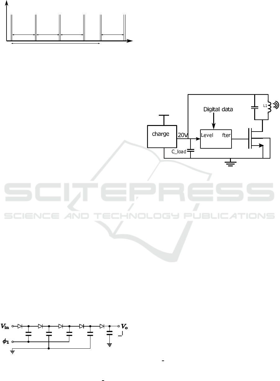
A Dickson charge pump has been designed for energy
storage in an off-chip 1 uF capacitor, C
load (Dick-
son, 1976).The high capacitance has been used to
store higher charge which is used to charge the induc-
tor L1 with high current. The charge pump charges
the load capacitor generating an output voltage of 20
V. The total time taken to reach the needed charge
is about 225 ms. An oscillator is used to generate a
clock with 50% duty cycle. Single clock was used in-
stead of a non-overlapping clock cycle in order to re-
duce the total power consumption of the charge pump
module as shown in figure 13.
The capacitor values for each stage of the charge
pump were chosen based on the available chip area
and the output power requirement for wireless data
transmission.
3.3V
pump
Shi
3.3V to 20V
C1
M1
Figure 14: Wireless data transmission.
3.3.2 Data Transmission
A block diagram of the wireless data transmission
module is shown in figure 14. A level shifter shifts
the voltage level of the digital data from 3.3 V to 20
V in order to drive the transistor. The 120V NMOS
output transistor M1 is connected to an off-chip res-
onance circuit load (L1 and C1). When the digital
data is HIGH, then NMOS is turned on and the in-
ductor L1 starts storing energy. When M1 switches
off the inductor discharges through C1 generating a
magnetic field and a high voltage spike at the drain
of M1. 120V NMOS device has been choosen from
H35B4D3 AMS process to sustain this high voltage.
This magnetic field is detected by the external reader
hardware. The frequency of the data transmission is
dependent on the values of L1 and C1. The exter-
nal hardware uses a resonant circuit tuned to the data
transmission frequency.
At each pulse, when M1 turns off a high drain-
source voltage spike is created by the L1 inductor due
to the stored energy in the inductor as shown in fig-
ure 15. The slow decrease in the voltage level of
the pulses is due to discharge of the storage capaci-
tor (C
load) with each bit of transmission.
BIODEVICES 2016 - 9th International Conference on Biomedical Electronics and Devices
260

Figure 15: Drain-source voltage (Vds) of the M1 transistor.
4 CONCLUSIONS
An ASIC for wireless energy harvesting and wireless
data transmission for blood pressure measurement is
presented in this paper. The ASIC was fabricated
using 350 nm high voltage CMOS technology. The
fabricated chip is shown in figure 16. The chip has
an area of 2.3 mm x 1.3 mm and consumes approx-
imately 1 mW. The small dimension and low power
consumption of the chip makes it suitable for im-
plantable application. The chip is tested for wireless
power reception at a frequency of 4 MHz. Clock ex-
traction from the wireless power is used for the digital
module and the communication between the chip and
the CDC.
Forward error correction was implemented to im-
prove data integrity and to save area on the chip by
avoiding extra circuitry for wireless data reception.
The analog muliplexerextends the functionality of the
CDC chip to support four pressure sensors instead of
one.
Digital
Charge Pump
LDO
Rectifier
Data
Transmission
Address
pins
120V NMOS
Figure 16: Fabricated ASIC (2.3mm x 1.3mm).
The chip has been tested and development of a
wireless blood pressure sensing implant is in progress
for EVAR and in-vivo test.
ACKNOWLEDGEMENTS
The authors gratefully acknowledge the support of
this work by a grant from the Federal Ministry of Edu-
cation and Research (BMBF, ESiMed [16 M3201D]).
REFERENCES
Bradford, B., Krautschneider, W., and Schr¨oder, D. (2010).
Wireless Power and Data Transmission for a Pressure
Sensing Medical Implant. In BMT 2010, Proceedings
of the Biomedizinische Technik Conference.
Corriere, M. A., Feurer, I. D., Becker, S. Y., Dattilo, J. B.,
Passman, M. A., Guzman, R. J., and Naslund, T. C.
(2004). Endoleak following endovascular abdominal
aortic aneurysm repair: implications for duration of
screening. Annals of Surgery, 239(6):800.
Dickson, J. F. (1976). On-chip high-voltage generation in
MNOS integrated circuits using an improved voltage
multiplier technique. Solid-State Circuits, IEEE Jour-
nal of, 11(3):374–378.
Drury, D., Michaels, J., Jones, L., and Ayiku, L.
(2005). Systematic review of recent evidence for
the safety and efficacy of elective endovascular re-
pair in the management of infrarenal Abdominal Aor-
tic Aneurysm. British Journal of Surgery, 92(8):937–
946.
Koops, A., Bradford, B., Schroeder, D., Krautschneider, W.,
Adam, G., and Buhk, J. (2013). Abstract No. 416-An
integrated stent-graft for noninvasive 4-dimensional
aneurysm sac pressure monitoring after endovascular
aortic aneurysm repair (EVAR): First in vivo results
in a porcine model. Journal of Vascular and Interven-
tional Radiology, 24(4):S176.
Kotani, K. and Ito, T. (2007). High efficiency CMOS
rectifier circuit with self-Vth-cancellation and power
regulation functions for UHF RFIDs. In Solid-State
Circuits Conference, 2007. ASSCC’07. IEEE Asian,
pages 119–122. IEEE.
Kotani, K., Sasaki, A., and Ito, T. (2009). High-efficiency
differential-drive CMOS rectifier for UHF RFIDs.
Solid-State Circuits, IEEE Journal of, 44(11):3011–
3018.
Milliken, R. J., Silva-Mart´ınez, J., and S´anchez-Sinencio,
E. (2007). Full on-chip CMOS low-dropout voltage
regulator. Circuits and Systems I: Regular Papers,
IEEE Transactions on, 54(9):1879–1890.
Silverstein, M. D., Pitts, S. R., Chaikof, E. L., and Bal-
lard, D. J. (2005). Abdominal aortic aneurysm
(AAA): cost-effectiveness of screening, surveillance
of intermediate-sized AAA, and management of
symptomatic AAA. Proceedings (Baylor University.
Medical Center), 18(4):345.
Spink, C., Buhk, J., John, B., Krautschneider, W.,
Schroeder, D., Fischbach, R., Braunschweig, M.,
Adam, G., and Koops, A. (2015). Integriertes, ka-
belloses, 4-dimensionales Druckmonitoring nach En-
dovaskularer Aortenreparatur (EVAR): Erste in-vitro
Wireless Energy and Data Transmission ASIC for Blood Pressure Measurement in an Aneurysm Implant
261

Ergebnisse im Gef¨aßmodel. In R¨oFo-Fortschritte auf
dem Gebiet der R¨ontgenstrahlen und der bildgeben-
den Verfahren, volume 187, page RK
WISS401 6.
Tej, P. R. and Jhansi Rani, K. (2013). VHDL Implementa-
tion of Reed Solomon Improved Encoding Algorithm.
International Journal of Research in Computer and
Communication Technology (IJRCCT), 2(7):435–439.
ZMDI (2015). ZSSC3123, http://www.zmdi.com/zssc3123.
BIODEVICES 2016 - 9th International Conference on Biomedical Electronics and Devices
262
