
Simulation Model of a SiC Power MOSFET
Variables Estimation and Control of a Power Source
E. Baghaz, N. K. M’Sirdi, K. Frifita, A. Naamane and M. Boussak
Aix Marseille Universit´e, CNRS, ENSAM, Universit´e de Toulon, LSIS UMR 7296, 13397, Marseille, France
LSIS UMR 7296 and HyRES Lab, RMEI, France
Keywords:
Electro-thermal Model, Boost DC/DC Converter, Power Source, SiC MOSFET Behavior, Estimation and
Control.
Abstract:
An electro-thermal model of a power SiC MOSFET is proposed. The thermal model, is coupled with the
physical model through the interaction between the transistor power loss and the junction temperature. For
validation of this model, the simulation curves are compared to the manufacturer’s experimental curves. As
first application, a boost DC/DC converter is considered. An observer is proposed to estimate the MOSFET
voltage V
DS
, the power and the junction temperature. These estimates are used to control the converter. The
proposed model and estimator give sufficiently good temperature and power estimation. The Power source
obtained using DC/DC converter is efficient, allowing the power loss reduction and robust.
1 INTRODUCTION
SiC MOSFET devices have a wide operation ranges
in voltage, current and temperatures, then the knowl-
edge of their characteristics and disposal of a good
model become necessary . As wide as is the model
validity domain, more and more high can be the con-
trol precision to achieve a high efficiency (Maxim and
Maxim, 1999; Pushpakaran et al., 2015). A simple
analytical PSpice model for SiCMOSFET have been
proposed for high power modules in (Johannesson
and Nawaz, 2016). In this paper we are interested
by the SiC MOSFET C2M0025120D CREE (1200V,
90A), when operating at very high frequencies.
The MOSFET device characteristics can be ex-
tracted from manufacturer’s experimental curves
(data sheets). Simulations are very important in elec-
tric systems design as well as for mechatronics case
study. Prototyping is necessary for the optimization
of power electronic circuits. To get realistic simula-
tions and accurate results, we need good and precise
models for an operating domain as wide as possible
(Leonardi et al., 1997).
The models proposed in the well known simu-
lation softwares like Psim, Pspice, LMS AMESIM,
Saber and other are often limited in their precision,
field of application or complexity. The most of them
are piece-wise linear. They are very, often valid
only in a restricted area and must be completed us-
ing the components Data Sheet. To get reliable re-
sults based on simulations, we need accurate models,
with acceptable precision.The precision of these mod-
els are very often limited to some operational points
or region. The devices may be, in some applica-
tions, used in very wide operation ranges (Bejoy et
al., 2015a)(Bejoy et al., 2015b).
In this paper, we propose an electro-thermal be-
havior model of a Silicon Carbide MOSFET (SiC).
The electrical behavior sub-model is based on the
well known EKV MOSFET Model (see (Enz et al.,
1987)). Then a thermal dissipation model, expressed
like Resistance-Capacitance (RC) Foster network, is
coupled to the electrical model. The lost power con-
tributes to the heating of the MOSFET internal junc-
tion. The heat transfer is described by a Foster elec-
trical equivalent network.
For validation of this model, the simulation curves
are compared to the manufacturer’s experimental data
(curves of data sheets).
The efficiency of the PhotoVoltaic (PV) system,
obtained using this DC/DC converter and the pro-
posed control, is robust against temperature varia-
tion. When Temperature varies from 25
◦
C to 150
◦
C,
the PV system efficiency is reduced globally by only
4%.The SiC MOSFET power loss is analyzed to re-
duce its effect on the PV source efficiency.
M’Sirdi, N., Baghaz, E., Frifita, K., Naamane, A. and Boussak, M.
Simulation Model of a SiC Power MOSFET - Variables Estimation and Control of a Power Source.
DOI: 10.5220/0006460806370643
In Proceedings of the 14th International Conference on Informatics in Control, Automation and Robotics (ICINCO 2017) - Volume 1, pages 637-643
ISBN: 978-989-758-263-9
Copyright © 2017 by SCITEPRESS – Science and Technology Publications, Lda. All rights reserved
637
2 SiC MOSFET BASED SOURCE
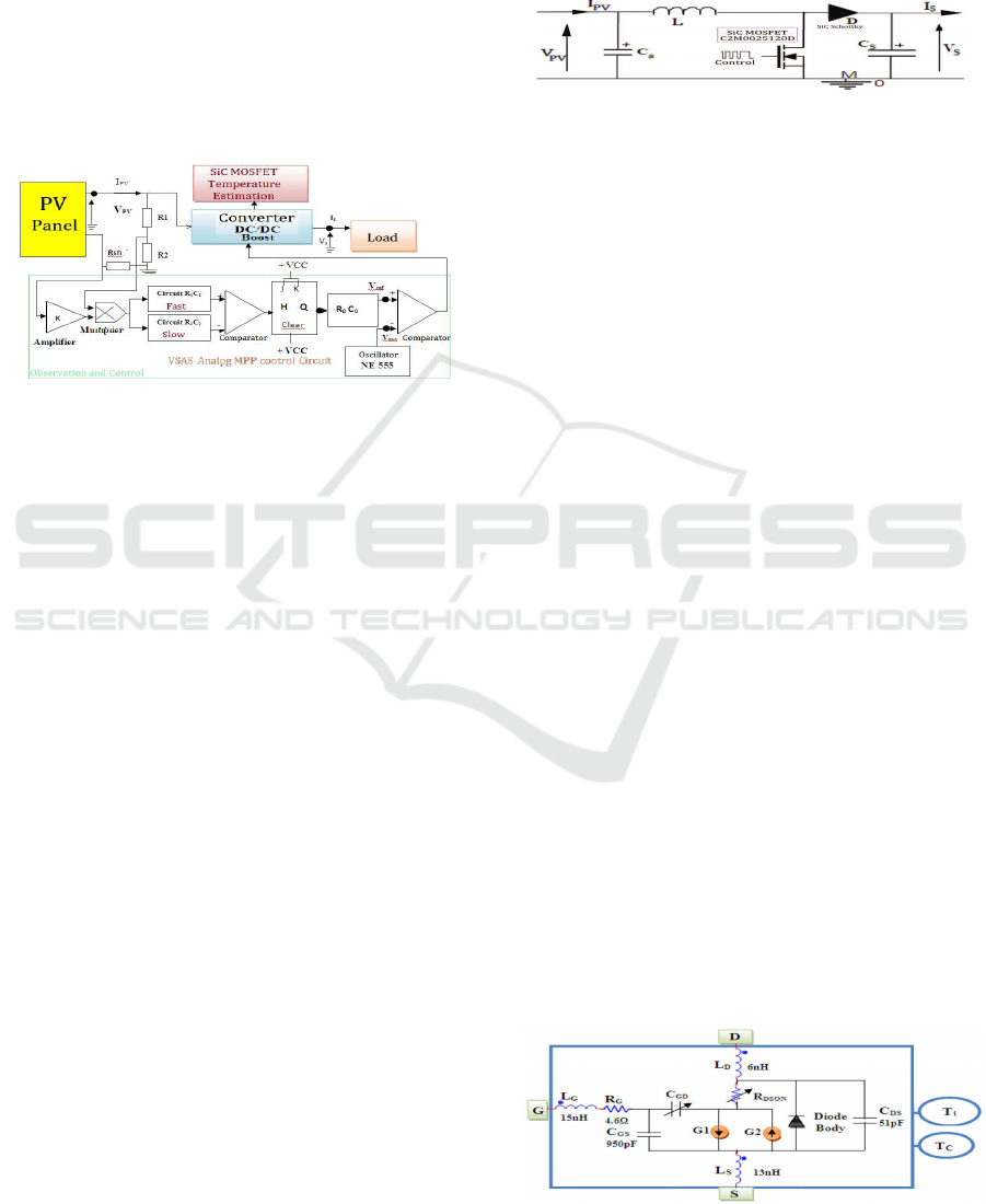
2.1 System Description
As a first application using this SiC MOSFET model,
we consider an energy source (PV panel) connected
trough a boost DC/DC converter driven by an analog
MPPT based control, with as load a 50Ω resistance.
This device is used to control a PV panel (PV S75),
see figure (2.1). The proposed control system is ana-
log to avoid the use of a computer based architecture.
Figure 2.1: PV source and Boost converter.
We have developed an analog circuit which esti-
mates, on the fly, the needed MOSFET voltage, the
power dissipated and the Junction temperature.
2.2 DC/DC Conversion with a SiC
MOSFET
In DC/DC converters, the most important power loss
is due to the ON and OFF switching transition. The
losses are proportional to the switching frequency
and the values of the parasitic capacitances of power
MOSFET component. So the characteristics ot the
SiC MOSFET used for commutation are of main im-
portance (Time of response, Rdson,...).
The efficiency of the PV system depends on
the used power converter and the control robust-
ness against temperature variations and perturbations.
When Temperature varies form 25
◦
C to 150
◦
C, the
PV system efficiency is reduced and the system char-
acteristics are perturbed.
This led us to choose a recently proposed SiC
MOSFET which can operate under high frequen-
cies and temperature condition. The SiC MOSFET,
C2M0025120D, proposed by CREE is studied and
used in a PV system (Figure 2.1 and 2.2) which is
composed by:
- PV panel SP75 which can generate a voltage
V
PV
=13V a current I
PV
=4.2A and a power P
PV
=55W
- DC/DC Boost using the SiC MOSFET proposed
by CREE: C2M0025120D, operating at a control fre-
quency f=10kHz (Figure 2.2),
- a Schottky diode C3D04060,
- an analog circuit used to estimate the MOSFET
junction temperature, as proposed in this paper,
- an analog circuit proposed for the MPPT control,
- The system load is resistance R
L
=50Ω.
Figure 2.2: DC/DC Boost Converter.
3 DYNAMIC MODEL
The model is developed for the SiC MOSFET and is
included to PSpice simulation software library. The
electrothermal behavior of SiC MOSFET is analyzed,
modeled and simulated under PSpice software.
3.1 SiC MOSFET Component Model
In a DC/DC converter the most important component
is the MOSFET which is subject to the perturbations
and thermal effect. Switching transition at high fre-
quency (to control the input and output signals) lead
to power dissipation and heating of the system. Ther-
mal flux propagation will then impact the circuit be-
haviour. This is mainly due to the signals distortions
(PWM) and parasitic impedance. A good behavior
model is needed to describe the MOSFET dynamics.
3.1.1 SiC MOSFET Electric Model
In figure 3.1, we present the model we have developed
for and implemented under Pspice, to simulate the the
SiC MOSFET C2M0025120D proposed by CREE.
Note that this model is more precise, with regard
to the LTspice model proposed by the manufacturer
CREE (Bejoy et al., 2015b) (Bejoy et al., 2015a), as
it is composed by 2 switched current sources.
In addition it takes into account package parasitic
inductances (L
G
, L
D
, L
S
) connected to the gate, drain,
source and resistances (R
G
, R
DSon
). The inductances
and resistances allow description of power losses in
Figure 3.1: Model of a SiC MOSFET.
ICINCO 2017 - 14th International Conference on Informatics in Control, Automation and Robotics
638

commutations. The resistance R
G
describes the Gate
power losses in high frequencies operation.
α and n define the triode r´egion and λ is the length
of the MOSFET conduction channel. The gate thresh-
old voltage is noted V
th
.
The output current I
DS
= I
G1
- I
G2
(Enz et al.,
1987).The MOSFET equations (V
DS
, I
DS
, R
dson
,
V
GS
...) are the following
I
DS
= I
G1
(V
p
−V
s
) − I
G2
(V
p
−V
D
) (1)
I
G1
= I
S
∗ (Ln(1 + exp
V
p
−V
s
2U
T
))
2
(2)
I
G2
= I
S
∗ (Ln(1 + exp
V
p
−V
D
2U
T
))
2
(3)
Where V
S
, V
G
, V
D
are the source, gate and drain
voltages of the MOSFET, respectively. V
p
=
(VG−U
T
)
K
s
is the pinch-offvoltage and Is = 2∗U
2
T
∗ K
s
∗ g
m
is the
specific current (g
m
is a trans-conductance and K
s
a
slope factor). The model equations are in function of
the MOSFET junction temperature. U
T
is the thermo-
dynamic voltage.
3.1.2 Thermal Model
To describe the thermal behavior, expressing that the
power losses are dissipated heating the MOSFET
junction which has thermal exchanges with the case
and the component environment, we consider a Fos-
ter’s RC network. We use 14 RC cells to describe the
thermal coupling. The junction and case temperatures
T
j
and T
C
are related through the thermal impedance
Z
TH
and depend on the power losses P
Perte
(see figure
3.2).
T
j
= T
C
+ P
Perte
∗ Z
TH
z
TH
=
14
∑
i=1
R
i
∗ (1 − exp
−t
R
i
C
i
)
(4)
Figure 3.2: Thermal propagation model.
3.2 Simulations and Model Validation
The developed model has been implemented in Saber,
Pspice, Psim and Matlab softwares and compared to
the experimental curves presented by the SiC MOS-
FET data sheet for its validation (Mudholkar et al.,
2015). The figure3.3compares the Drain-Source cur-
rent (I
ds
) versusthe MOSFET output voltage (V
DS
) for
several Gate-Source voltages (V
gs
) under a tempera-
ture of 25
◦
C. Simulation results (continuous lines) are
in good aeement with the data sheet values (bars).
Figure 3.3: I
DS
and V
DS
for different V
GS
.
- For V
GS
values less than 4V, the MOSFET is
not controlled because the threshold voltage V
th
is not
reached. When the MOSFET start operation V
GS
>
V
th
> 4V, and then the current I
DS
increases gradually
with V
GS
. The results are in good agreement.
The figure 3.4 shows the simulated and the ac-
tual Drain-Source resistance (R
dson
) in function of the
temperature variation for a current equal to I
DS
=50A
and voltage V
GS
=20V. The obtained curves are very
close in a wide temperature range (up to T=150
◦
C).
In conclusion, the proposed electrothermal model
is very accurate and able to describe the dynamic be-
havior of the SiC MOSFET with a very good preci-
sion.
4 ESTIMATION AND CONTROL
4.1 Observer for Variables Estimation
As seen in figure 3.5 the variation of the resistance
R
DSon
in function of the temperature T
j
can be approx-
imated by the following equation:
R
DSon
(T
j
) = R
DSon(300
◦
K)
(1+
α
100
)
(T
j−300
)
V
DS
= ζ.(R
DSon
(T
j
)).I
D
(5)
Let us introduce the variable ζ to account for the
variable structure feature of the system. ζ = 0 means
that the MOSFET is off and ζ = 1 means that it is on.
The junction temperature T
j
grows with the MOSFET
Figure 3.4: Variation of R
dson
versus the temperature T
j
.
Simulation Model of a SiC Power MOSFET - Variables Estimation and Control of a Power Source
639

Figure 4.1: R
dson
in function of the temperature T
j
.
output voltageV
DS
and powerlosses. In the figure 4.1,
we note that the relation betweenV
DS
and T
j
is almost
linear.
For parameters estimation and variables observa-
tion we can consider a first order (linear) regression
model, during the period where the MOSFET is on.
The solid line (in red) of the figure ?? confirms, from
the simulations and data sheet experiments, the good
precision of this approximation. Thus we cant write.
V
DS
= A∗ T
j
+ B (6)
From the simulation result of figure 4.1, we can
deduce by estimation that A = 0.001666 and B =
0.285 and then we can consider to estimate the junc-
tion temperature in average by T
j
=< (V
DS
− B)/A>.
4.1.1 Estimation of Electric Variables
The subsystem model is obvious if we take P = V.I as
output and the current and voltage as inputs. Let us
consider the estimations of the PV panel voltage
ˆ
V
PV
and current
ˆ
I
pv
. These estimations are implemented in
the circuit of figure (2.1). The small shunt resistor R
sh
gives us an image of the current by the voltage V
r
and
an image of the PV voltage is produced by the bridge
of resistances R
1
and R
2
.
V
r
= a
1
.
ˆ
I
κv
= I
pv
∗ R
sh
V
p
= a
2
.
ˆ
V
PV
=
R
2
R
1
+R
2
∗V
pV
(7)
The estimation of the instantaneous PV power is
needed for the control, at two time instants t
1
and t
2
,
in order to estimate its gradient. We can then deduce,
using a signal multiplier, the produced PV power by
ˆ
P =
ˆ
V
PV
.
ˆ
I
pv
.
It remains now to estimate the power difference
between two time instants. This can be done through
two different time delays circuits τ
1
= R
1
C
1
and τ
2
=
R
2
C
2
to get the delayed power estimations
ˆ
P
1
and
ˆ
P
2
and their difference △P =
ˆ
P
1
−
ˆ
P
2
, using a signal
comparison component.
4.1.2 Observer for Temperature Estimation
The Drain-Source voltage (V
DS
) must be estimated
when the MOSFET turns ON (ζ = 1 means that the
MOSFET state is ON). To get, in practice, the vari-
able ζ which accounst for the MOSFET state we use
an additional MOSFET (T
2
) connected to to Gate and
Figure 4.2: Estimation of the state Variables.
the Drain of the previous MOSFET. As shown in fig-
ure 4.2, T
2
is controlled by the same PWM signal and
receives the voltage V
DS
.
Its source is connected to a capacitance C to which
it transmits the voltage v = ζ.V
DS
. Then the MOSFET
T
2
controls the charge of the capacitance C, under the
voltage V
DS
(when it is ON ζ = 1 ). When the capaci-
tance is charged, the voltage will reach the value
ˆ
V
DS
,
as an estimation of the Drain-Source voltage V
DS
). Its
discharge will be slow as it is connected to an Opera-
tional Amplifier, in the other side (when ζ = 0). Then
it will keep the estimation
ˆ
V
DS
.
The next estimations are obviously produced by
an inverse-amplifier (defined with the resistances
R
1
, R
2
, R
3
and R
4
) and a signal multiplier to get
V
s
=
ˆ
V
DS
− B and V
f
=
ˆ
T
j
=
1
A
Vs = T
j
(8)
Then we are able to develop analog estimations of
the voltages
ˆ
V
PV
, and
ˆ
V
DS
, current
ˆ
I
pv
, the power
ˆ
P
1
at t-τ
1
and
ˆ
P
2
at t-τ
2
and their difference △P =
ˆ
P
1
−
ˆ
P
2
,
with in addition the temperature
ˆ
T
j
.
4.2 Control Circuit (MPPT)
The behavior of the conversion systems of this kind
of renewable energy is VSAS (Variable Structure Au-
tomatic Systems) and highly dependent on variations
in climate parameters, such as temperature and irra-
diation. The MPPT algorithms are expected to maxi-
mize, at each time instant, the produced power. Sev-
eral techniques have been designed to search this op-
timal MPP. In figure 2.1, we propose and analog cir-
cuit which produces the MPPT control signal as given
by the algorithms developed in our previous work
((M’Sirdi et al., 2014)).
If the PV panel power increases or
decreases(∆P ≥ 0 or ∆P ≤ 0), the JK Flip-Flop
state changes correspondingly. The flip-flop output
Q is used to produce a triangular signal (V
ref
as
a reference for commutation) and then the PWM
required for the MOSFET control. The reference
signal frequency is fixed to 10kHz, by means of the
choice of τ
0
= R
0
C
0
the integrator time constant. V
ref
allows to adjust the duty factor.
ICINCO 2017 - 14th International Conference on Informatics in Control, Automation and Robotics
640
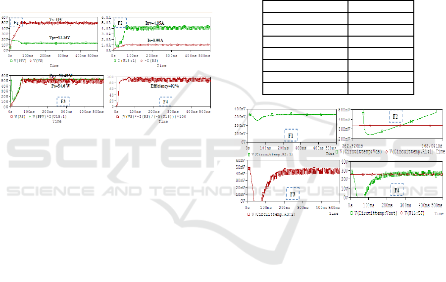
4.3 Simulation Results and Discussion
4.3.1 The PV Control System Simulation
The PV system, described in section 2, plus the esti-
mation and control circuits of section 4, are simulated
under the physical modeling oriented software Pspice.
The irradiation is considered, for the first simu-
lation, fixed at 100W/m
2
with the temperature T
j
=
25
◦
C. The proposed control generates a good PWM
signal with as duty factor 0.7. In the same figure 4.3-
F1 and F2 show the voltage and current of the PV
panel in green (V
pv
,I
pv
) and the outputs of the DC/DC
converter (V
s
,I
s
).
Figure 4.3: Global PV system electric variables.
The PV output voltage is V
pv
= 13.36V. The
DC/DC output voltage is V
s
=49V>V
pv
, and the cur-
rent is I
s
= 0.99A < I
PV
= 4.05A.
The figure 4.3-F3 shows that the PV output power
P
pv
= 54,6W (in green) is practically completely
transmitted by the DC/DC converter to the load P
s
=
50,43W (in red). The instantaneous powers (P
pv
, P
s
)
oscillate in the neighborhood of the Maximum Power
Point (F3 and F4). The global PV system has an effi-
ciency equal to η = 92% (see figure 4.3-F4). In figure
4.3-F1 (respectively F2) we show the voltages (cur-
rents) at converter input DC/DC Boost V
PV
(I
PV
in
green) and output Vs (Is in red). Figure 4.3-F4 shows
the overall performance of the PV system.
The PWM signal produced by our control MPPT
circuit allows us to retrieve the MOSFET state
(On/Off) giving a very good estimation of the infor-
mation signal ζ. This signal is important for the es-
timation of V
DS
. It allows us to distinguish the pe-
riod where the MOSFET (C2M0025120D) is OFF
and when it is ON. When the MOSFET state is ON
ζ = 1, the estimated voltage
ˆ
V
DS
converges to the
MOSFET one V
DS
. When the state MOSFET is OFF
ζ = 0, the second MOSFET T2 is also OFF (as it re-
ceives the same PWM signal). The estimated voltage
ˆ
V
DS
is kept, more or less, constant by the capacitance
C.
This proves the efficiency of the proposed SASV
MPPT control algorithm combined whit the proposed
estimation circuits.
4.3.2 Thermal Behavior and Temperature
Estimation
Simulations have been done for different values of the
studied MOSFET junction temperature going from
25
◦
C up to 110
◦
C. The estimated temperatures are
presented in table 1. We can remark than the maxi-
mum error is 3
◦
C.
Table 1: The estimated temperatures.
T
j
MOSFET SiC
◦
C Estimated (
◦
C)
25 25
30 31
40 39
50 47
75 72
100 100
110 112
Figure 4.4: Signaux des diff´erents g´en´er´es par diff´erents
blocs de circuit de temp´erature.
The estimated voltage is V
DS
=320mV (see figure
4.4-F1 in green), The voltage Vds acquired (in Fig-
ure 4.4-F2 in red) equals the average value of actual
the voltage Vds of the investigated transistor, during
his On state (see figure 4.6-F2 in green), justifying
good Vds earned value. The output voltage of the am-
plifier of figure 4.2 Subtractor is 40mV order (Figure
4.4-F3), which shows that the constant B in equation
6 equals 280mV. Finally F4 compares the MOSFET
temperature T
j
(in green) to its estimation given by
the thermal model (in red).
The investigated transistor temperature is of the
order of 25.45
◦
C (Figure 4.6-F4), in other words, the
transistor switches under a room temperature, which
confirms the good functioning of the overall PV sys-
tem. Temperature issued by the circuit developed dur-
ing this work is identical with that given by the ther-
mal model of the MOSFET in figure 2, with a differ-
ence less than 0.2
◦
C.
Simulation Model of a SiC Power MOSFET - Variables Estimation and Control of a Power Source
641

Table 2: Influence of Temperature on efficiency.
Temperature C2M0025120D Efficiency of PV system
25
◦
C 92%
50
◦
C 90%
75
◦
C 89.93%
100
◦
C 88.9%
125
◦
C 88.5%
150
◦
C 88%
4.3.3 Power Losses in the PV System
As already mentioned DC/DC power converters suf-
fer from loss of power loss due to components heat-
ing. In this context, we have studied the influence of
the temperature on the MOSFET Characteristics.
The table2 summarizes the results obtained when
the junction temperature increases from 25
◦
C to 150
◦
C. The system performancedecreases of 4%. Which
shows that the monitoring of the MOSFET temper-
ature, in a power converter is necessary to reduce
power losses.
In order to show performance degradations when
the MOSFET is poorly controlled (deformation of the
PWM signal), we compare the simulation results in
figure 4.8 to the normal situation (when the MOSFET
is controlled by a PWM signal without deformation
Figure 4.3-F1). F1 shows a distorted signal of PWM
and F2 the junction temperature.
Note that this study was conducted on the same
PV system, under the same climate conditions,
namely a 1000W/m
2
irradiance and a temperature of
25
◦
C. When the MOSFET of the DC/DC Boost con-
verter is controlled by a deformed PWM signal (Fig-
ure 4.5-F1), its temperature rises to 30
◦
C (Figure F2)
instead of 25
◦
C in normal operation case (Figure 4.3
F4). That is to say a temperature increase of 16.66%
leads to the overall performance from 92% (during
normal operation) down to 73.8% (Figure 4.8-F3).
This represents a decline of efficiency of 18.2%.
Figure 4.5: Effect of a deformation in PWM signal.
5 CONCLUSIONS
An electro-thermal model of a power SiC MOSFET is
proposed for efficient circuits simulation. This model
describes the links of the various physical parame-
ters of the MOSFET (Vds, Ids, Tj...), which clarify
the electrical and thermal coupling. This allows to
get more realistic simulations. To validate the pro-
posed model equations and parameters, we have com-
pared simulation results with those of datasheet of the
MOSFET. It appears that the electro-thermal model
has high accuracy even in high temperatures and high
voltages.
Then, we have developed a circuit that gives mea-
sures and estimates of the system state variables and
the junction temperature of the MOSFET. The com-
parison of the temperature of the thermal model of
the MOSFET with that of the developed estimation
circuit shows that there is a good agreement. In or-
der to show the good convergence of the estimates,
we have used this power componet in a DC/DC Boost
converter for adaptation between a PV source and a
50Ω resistive load.
The converter is controlled by an analog MPPT
control proven to be efficient, fast and robust. Then
we have studied the influence of the temperature on
the overall performance of the same PV system. It
appears that by varying the temperature of the junc-
tion of the transistor from 25
◦
C to 150
◦
C, the over-
all performance of the PV system decreases by 4%.
In the same work, we consider also the effect of de-
formation on the PWM signal and we show how the
system performance degrades.
The PV system with DC/DC converter control is
investigated using Pspice. The results show that the
proposed model is the most precise compared to all
the literature existing models. An analog circuit ob-
server is then implemented. The control based on the
observer estimations is also implemented as an analog
circuit. This model can be used for simulation of any
application using this SiC MOSFET into Pspice soft-
ware. The simulation results show that the proposed
model is efficient, reliable and show that our electro-
thermal model approach and the proposed estimator
give good temperature estimation and control.
ACKNOWLEDGEMENTS
This research is activity is held by the SASV group of
the LSIS and funded by the BPI in a FUI projects.
Special aknowledgements are addressed to all our
project partners.
ICINCO 2017 - 14th International Conference on Informatics in Control, Automation and Robotics
642

REFERENCES
Bejoy, N., Pushpakaran, N., Stephen, B., Bayne, B., Wang,
G., and Mookken, J. (2015a). Fast and accurate
electro-thermal behavioral model of a commercial sic
1200v, 80 mohm power mosfet. IEEE Transactions
on Electron Devices.
Bejoy, N., Pushpakaran, N., Stephen, B., Bayne, B., Wang,
G., and Mookken, J. (2015b). A simple approach
on junction temperature estimation for sic mosfet dy-
namic operations within safe operating area. IEEE
Transactions on Electron Devices, 12.
Enz, C., Krummenacher, F., and Vittoz, E. (1987). A cmos
chopper amplifier. IEEE Journal of Solid-State Cir-
cuits, 22.
Johannesson, D. and Nawaz, M. (2016). Analytical pspice
model for sic mosfet based high power modules. Mi-
croelectronics Journal, 53:167-176. QC 20170410.
Leonardi, C., Raciti, A., Frisina, F., , and Letor, R.
(1997). A new pspice power mosfet model with
temperature dependent parameters: evaluation of per-
formances and comparison with available modelsl.
Thirty-Second Conference Record of the 1997 IEEE
IAS Annual Meeting, IAS97.
Maxim, A. and Maxim, G. (1999). A high accuracy power
mosfet spice behavioral macromodel including the de-
vice selfheating and safe operating area simulation.
40th APEC Dallas.
M’Sirdi, N., Nehme, B., Abarkan, M., and Rabbi, A.
(2014). The best mppt algorithms by vsas approach
for renewable energy sources (res). In EFEA 2014,
pages 1-7, Paris France.
Mudholkar, M., Ahmed, S., Ericson, M., Frank, S. S., Brit-
ton, C. L., and Mantooth, H. A. (2015). Datasheet
driven silicon carbide power mosfet model. IEEE
Transactions on Power Electronics.
Pushpakaran, B., Bayne, S., Wang, G., and Mookken, J.
(2015). Fast and accurate electro-thermal behavioral
model of a commercial sic 1200v 80 mohms. IEEE
Pulsed Power Conference (PPC).
Simulation Model of a SiC Power MOSFET - Variables Estimation and Control of a Power Source
643
