The Method to Measure Si Thickness for Bond Line Thickness
YangSub Park, KilBum Kang, Sangyun Yun and SeongSoo Kim
Advanced Technology Inc, Incheon, Korea
Keywords: BLT, Bond Line Thickness, Si Thickness, TSV.
Abstract: Today, many semiconductor products are manufactured through the TSV process. At this time, It is
important to manage the Bond Line Thickness because all of the stacked dies must be discarded due to a
single contact failure. If we can measure the thickness of the silicon, the BLT in the wafer level package
process can be estimated. In this paper, we propose a method to measure the thickness of silicon by using
infrared ray. We designed the infrared light source to select the path of the incident light to the objective
lens. And this optical system has a characteristic of moving in the opposite direction according to a change
in height. By using this optical system, it is possible to calculate the correct in-focus position. By doing this,
we present a method to measure BLT by measuring the distance between the top and bottom of Si surface.
1 INTRODUCTION
The Bond Line Thickness (BLT) is one of important
measurement items for 3D Integrated Circuits (IC)
(Patti, 2006) using Through Silicon Vias (TSV)
(Topol et al, 2006) because each chip in the product
is directly connected in the vertical direction. When
the distance between the layers is increased, The
defects such as a head in pillow (HIP) (Liu et al,
2010) (Son et al, 2016) may occur. These types of
defects may weaken the electrical connections and
reduce the reliability of the product. While it is
almost impossible to observe bond joint between
bump and pad, many semiconductor production
plants manage the BLT to ensure die attach quality
and reliability. However, even this method is
impossible in the Wafer Level Package (WLP)
process. Because it is difficult to measure the BLT
sideways because of the neighboring dies.
Therefore, we propose a method to measure the
thickness of Si without destroying the mass
production products. And the BLT in WLP can be
measured using this method.
2 METHOD
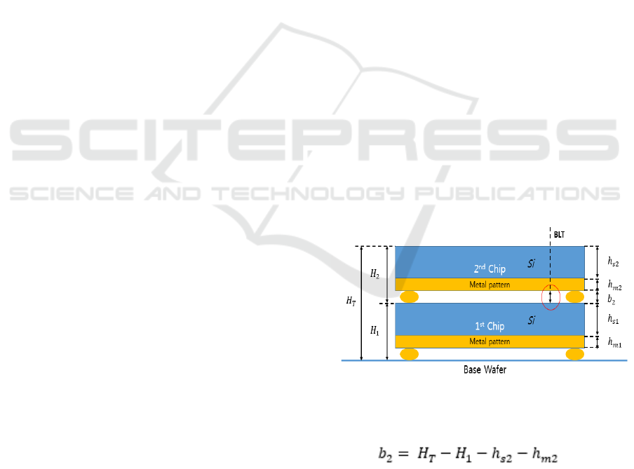
Figure 1 is the cross-section diagram of chips
stacked on the base wafer. The chip consists of a Si
layer and metal layers. H is the height of the chip
from the base wafer or a previous chip. h_m is the
thickness of metal layers of H and h_s is the Si
thickness of H. b_2 is BLT and it means the space
between chips. The height of chip is sum of Si layer,
the height of metal layers and the thickness of bond
line. It is possible to calculate b. Generally, the
thickness of metal layer is almost the same as the
design value. And there are many methods to
measure H. Therefore, The BLT in WLP can be
estimated by accurately measuring the Si thickness.
Figure 1: The cross-section diagram of chips stacked on
the base wafer.
(1)
2.1 The Design of Optic
We designed an infrared optical system to measure
the thickness of Si without damaging the wafer and
chips. Infrared ray has good light transmission
property for silicon, so we can get the images
Park, Y., Kang, K., Yun, S. and Kim, S.
The Method to Measure Si Thickness for Bond Line Thickness.
DOI: 10.5220/0006525502730275
In Proceedings of the 7th International Conference on Pattern Recognition Applications and Methods (ICPRAM 2018), pages 273-275
ISBN: 978-989-758-276-9
Copyright © 2018 by SCITEPRESS – Science and Technology Publications, Lda. All rights reserved
273

reflected by the opposite metal pattern through Si.
The light incident on the silicon is divided into a
signal reflected from the silicon surface and a signal
reflected after passing through the silicon. The
thickness of the silicon can be measured through the
path difference between these two signals.
However, if the thickness of the chip is very large,
the gap between the two signals becomes large and it
is difficult to measure them simultaneously. And in
the opposite case, it is also not easy to measure the
distance between these two signals because they
overlap each other.
Figure 2: Left: a schematic diagram of an infrared optical
system, right: the light paths with focus change.
To solve these problems, we designed optical paths
of the light incident on the objective lens as shown
in Figure 2 left. This optical system has the
capability of confirming the position of the objective
lens and focus state.
Figure 2 left is a schematic diagram of the optical
system. It is possible to get the signals that move
inversely to each other when the focus change. The
results are shown in Figure 2 right. In the in-focus
state, the light of the two paths is met at one point.
However, when the focus changes up and down, it
moves away from each other.
2.2 Measurement of Si Thickness
Figure 3 is a schematic diagram of image acquisition
in silicon using the optical system of Figure 2. Since
the infrared light source penetrates the silicon,
infrared light be focused both the top surface of the
silicon and the bottom of it. D is the distance
between two different in focus position. h
s
can be
estimated by multiplying D and the coefficient of
refraction of silicon and the angle of incidence of the
beam.
Figure 3: The path of light with different focus position.
Figure 3 is an image acquired at regular intervals in
the height direction using the optical system of
Figure 2. I(x,y) is the brightness value at the (x, y)
pixel position of the image. And C is the y position
of the straight line existing in the image. In order to
measure C, we calculated the line profile in the y
direction and find the center of gravity using the
brightness of the image as the weight.
(2)
There are two straight lines in the image. C_1 is the
position of the straight line calculated in the area on
the left side and C_2 is the position of the straight
line calculated in the right image. F means how the
two straight lines match. This can be obtained from
equation (3). At this time, let P be the position where
F is the maximum value. This P means the position
of in focus.
(3)
n
1
is the refractive index in the air, and is the
refractive index of the silicon. P
t
is the point where F
is the maximum on the silicon top surface and P
0
is
the point where F is the maximum on the silicon
bottom surface.
ICPRAM 2018 - 7th International Conference on Pattern Recognition Applications and Methods
274

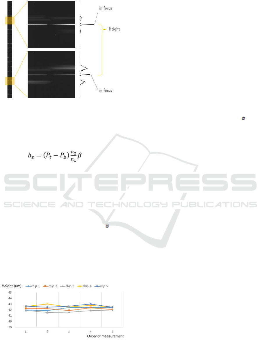
Figure 4: The image acquired from real sample.
And β is a coefficient according to the incident angle
of the beam. This is easily measurable using samples
already known in height. Therefore, the height of
silicon can be obtained via equation (4).
(4)
3 EXPERIMENT RESULTS AND
ANALYSIS
In order to measure repeatability, the same positions
were measured five times on each chip. Then, we
calculated the variance of these values, and multiply
this value by 3 to evaluate it on the 3 . The
repeatability average for these five chips is 0.67μm.
In order to measure the accuracy, We measured the
specific location of the chip five times. Then, the
position was measured with a high resolution
microscope and compared. The average accuracy
from 5 chips was confirmed at 0.32μm. This result is
shown in Figure 5.
Figure 5: The results of measurement.
4 CONCLUSIONS
An infrared optical system was used to measure the
thickness of silicon without destroying the wafer.
Infrared illumination was investigated so that the
path of light incident on the objective lens could be
selected and the focus state could be confirmed.
Then, the position of in-focus was calculated by
adjusting the height so that the left and right lines
match with the image acquired using this optical
system. These operations were performed from the
upper and lower surfaces, respectively, and the
height difference was calculated, and the actual
thickness was measured by multiplying this value by
the coefficient corresponding to the refractive index
of silicon and the incident angle of the beam. The
repeatability of the thickness of the silicon measured
in such a process is 0.67μm on the 3 . The
measurement accuracy was confirmed on average
0.32μm.
This value is three times better than the production
process control standard 2μm. Therefore, by using
the method proposed in this paper, it is possible to
manage BLT process of wafer level package
products.
REFERENCES
Patti, R.S. "Three-dimensional integrated circuits and the
future of system-on-chip designs", Proceedings of the
IEEE, Vol.94, Iss.6, pp. 1214- 1224
A. W. Topol, D. C. La Tulipe, Jr., L. Shi, D. J. Frank, K.
Bernstein, S. E. Steen, A. Kumar, G. U. Singco, A. M.
Young, K. W. Guarini, and M. Ieong, “Three-
dimensional integrated circuits,” IBM J. Res.
Develop., vol. 50, no. 4/5, pp. 491–506, Jul.–Sep.
2006.
Yan Liu; Pamela Fiacco; Ning-Cheng Lee “Testing and
prevention of head-in-pillow” 2010 5th International
Microsystems Packaging Assembly and Circuits
Technology Conference
Ho-Young Son; Tackeun Oh; Joo-Wan Hong; Byeong-Do
Lee; Ji-Hyuk Shin; Sung-Ho Kim; Nam-Seog Kim
“Mechanical and Thermal Characterization of TSV
Multi-chip Stacked Packages for Reliable 3D IC
Applications” 2016 IEEE 66th ECTC
The Method to Measure Si Thickness for Bond Line Thickness
275
