Fabrication of Aberration-corrected Diffraction Grating
for Soft X-ray Grating Monochromator
Yilei Hua Hailiang Li and Changqing Xie
Laboratory of Microelectronics Devices & Integrated Technology, Institute of Microelectronics,
Chinese Academy of Sciences, Beijing 100029, China
Keywords: Diffraction Grating, Nanofabrication, Monochromator.
Abstract: In this work, we present the design and fabrication of an aberration corrected diffraction grating for soft X-
ray monochromator. Spherical mirrors, which induce spherical, coma and astigmatic aberration, degrade the
performance of a grating monochromator. These aberrations are often corrected by aspherical mirrors.
however, aspherical mirrors with high surface accuracy are very difficult to fabricate. We proposed a new
diffraction grating, by carefully adjust the positions of grating lines, the wavefront of the diffracted light can
be modified and the aberrations can be corrected under certain conditions and the performance of the
monochromator can be improved. The aberrations of a typical Czerny-Turner monochromator are discussed
in detail and the grating design method is proposed in this work. A lamina type aberration corrected
reflective grating for soft X-ray is fabricated using e-beam lithography, and the detailed process is
elaborated.
1 INTRODUCTION
These days, experiments using soft X-ray are often
carried out with synchrotron radiation. To obtain
light with certain energy, grating monochromator is
often employed. (Saitoh, 2000; Chao, 2012) For a
grating monochromator, one key factor which can
affect the performance is the aberrations which can
deteriorate the image quality. (Noda, 1974; Shafer,
1964;
Reader, 1969)
In a monochromator which use spherical mirrors,
the major aberrations are spherical coma and
astigmatic aberration. At near-normal incidence a
concave spherical mirror can be used to form a good
image of a point object on the optical axis. However,
this is no longer the case as the object is moved
away from the optical axis, and the aberrations
become severe for grazing incidence angles.
(Mahajan, 1991)
In X-ray region, high reflectivity can only be
obtained at grazing angles of incidence. For the
refractive index of the reflecting medium is very
close to, and slightly less than, that of the vacuum
the total external reflection can occur only at grazing
incident angles. At grazing incidence angles, the
images are severely astigmatic, for a grazing angle
of about 2°, the sagittal focal length is about 1000
times the meridian focal length.
The traditional way to correct these aberrations is
using aspherical mirrors, spherical aberration can be
corrected by a paraboloid mirror, and astigmatic
aberration can be corrected by a toroidal mirror.
Aspherical mirrors with high surface accuracy are
very difficult to fabricate, and the cost is very high.
Another widely employed way to correct aberrations
is using toroidal grating, yet it is still difficult to
fabricate and the resolution is relatively poor for
they quickly go out of focus.
Diffraction gratings are often fabricated with
a ruling machine or interference methods. These
methods have their limitations, only strait or slightly
curved grating lines can be obtained. Nowadays,
with the development of nanofabrication methods,
the lamina type plane gratings are easier to fabricate
with lithographic methods, i.e. e-beam lithography
and UV lithography (Zhao, 2008). With these
methods, grating lines with arbitrarily shape and
positions can be fabricated easily. Thus the
wavefront errors introduced by spherical mirrors can
be compensated.
In this work, we proposed diffraction grating
with curved grating lines to correct the aberrations.
The relation between the wavefront and the position
110
Li, Y. and Xie, C.
Fabrication of Aberration-corrected Diffraction Grating for Soft X-ray Grating Monochromator.
DOI: 10.5220/0007312001100113
In Proceedings of the 7th International Conference on Photonics, Optics and Laser Technology (PHOTOPTICS 2019), pages 110-113
ISBN: 978-989-758-364-3
Copyright
c
2019 by SCITEPRESS – Science and Technology Publications, Lda. All rights reserved

of the grating line is analysed and the detailed design
method is discussed in section II. The fabrication
process of a soft X-ray laminar type diffraction
grating is discussed in section III.
2 GRATING DESIGN
In this work, we will discuss the grating used in a
Czerny-Turner monochromator, the structure is
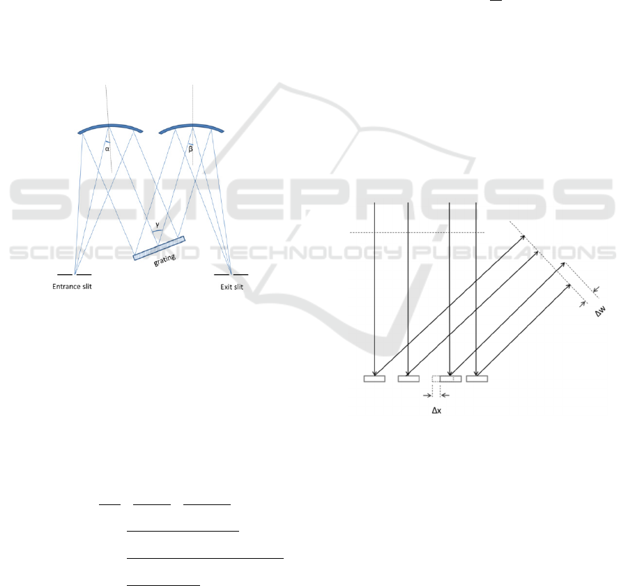
sketched in Fig. 1. This monochromator consists of
two spherical mirrors and a diffraction grating. Light
from the entrance slit is collimated by the first
mirror, then the collimated light is then diffracted by
the grating into different directions, and the light is
focused by the second mirror, light with different
wavelength is focused on the different positions on
the exit slit plane, only light with selected
wavelength can come out the exit slit.
Figure 1: The Czerny-Turner monochromator composed
of two spherical mirrors and a diffraction grating.
To correct the aberration, we first calculate the
aberration function of the monochromator. The pupil
is set on the grating plane. For simplicity, we
calculate primary aberrations only. The focal length
of the mirrors are F
1
and F
2
, the incident angle of the
chief ray on the two mirrors are α and β, the
coordinates on the grating surface are r and θ. The
primary aberration function can be written as:
w
r, θ; α, β, γ
32
4
2
32
4
2
(1)
The first and the fourth term represent spherical
aberration of the first and the second spherical
mirror, the second and the fifth term represent coma
and the third and the sixth term represent astigmatic
aberration.
With the aberration function, we can corrected it
by modify the grating. The principle is shown in
fig.2. We started with a traditional grating with
equally spaced grating lines. As shown in fig.2. By
displacing a grating line by Δx, the diffracted
wavefront is changed by Δw. According to
diffraction rules, the change of wavefront can be
written as.
∆w λn
∆
(2)
Where λ is the wavelength of the light, n is
diffraction order and d is the period of the grating
lines, respectively. While the aberration is different
from place to place on the grating, the displacement
of one grating varies and the grating line is curved.
With equation (1) and (2), we can get down to
draw the grating layout. As the grating lines are
curved and unequally spaced, it cannot be fabricated
by a traditional grating ruling machine. We use an e-
beam to fabricate this grating.
Figure 2: Modifying the wavefront of the diffracted wave
by displacing the grating line.
There are three types of X-ray diffraction
grating: (a) amplitude; (b) blazed; (c) laminar. In X-
ray region, light incident on the grating at a grazing
angle, the laminar type grating is the best type. In
principle, blazed gratings can be used to diffract all
of the incident intensity into a given order. However,
the blaze angle must be less than the incidence angle,
i.e., than the critical angle, and should be as small as
feasible in order to illuminate as much of the land as
possible. As the grating pitch becomes finer, less of
Fabrication of Aberration-corrected Diffraction Grating for Soft X-ray Grating Monochromator
111

the land is illuminated for a given incidence angle,
and the grating will become ineffective. Under this
circumstance, the laminar type is suitable.
3 FABRICATION
The grating is fabricated on a
152mm×152mm×6.35mm silicon plate. It is the
largest sample which our e-beam writer (JBX-
6300FS, JEOL, japan) can handle; and it can share
the same cassette with an industry standard 6025
mask. To get a flat surface, the thickness of the plate
is very important. The silicon plate was polished to
be very flat and very smooth, the surface flatness is
less than 60nm with in 100mm in diameter, and the
surface roughness is less than 0.5nm.
To reduce the writing time, we used SAL-601, a
negative tone, chemically amplified resist from the
Shipley Corporation, to pattern the grating. The
exposure dose of SAL-601 is about 20-50 uC/cm2,
much lower than that of PMMA or ZEP520A.
Consequently, the e-beam writing time is reduced to
about 70 hours.
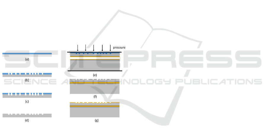
Figure 3: Process flow: (a) A 4 inch silicon wafer was spin
coated with a layer of negative tone photoresist SAL-601
(Shipley Corporation); (b) Lithography was performed
with a 100 kV e-beam writer (JEOL JBX-6300FS).
Photoresist was developed in CD26 after a 105 °C 3 min
PEB; (c) Silicon was etched by a high-density plasma
etching system (ULVAC NE550); (d) Photoresist was
removed by plasma etching with oxygen and the wafer
was diced into a 100mm×40mm slice by a laser dicing
machine. (e) The thin slice of grating was bonded to a
30mm thick bulk silicon. (f) The protective layer on both
side of the grating was removed and the surfaces were
cleaned thoroughly; (g) The surface of the grating was
coated with a thin layer of gold (50nm) by using a
magnetron sputtering system.
The process that we have implemented is
sketched in Fig. 3. The silicon plate is cleaned by
acetone, ethanol and DIW and is baked in an oven at
105℃ to remove moisture. It is spin coated with a
layer of SAL601, which is 500nm in thickness. The
photoresist was baked in an oven for 30 minutes at
105℃ to remove solvent in the photoresist. A JBX-
6300FS (JEOL japan) e-beam writer is used to
pattering the gratings, at 2 nA e-beam current, it
takes about 70 hours to pattering the gratings.
For a chemically amplified resist, the post
exposure bake (PEB) is a very critical process. The
PEB temperature affects the line width of the
photoresist and the PEB time affects the thickness of
the residue resist. After many times of experiment,
the PEB temperature is set to 105℃ and the PEB
time is 30 minutes. After PEB, the photoresist was
developed in CD26 for 3-5 minutes. The pattern
on the photoresist needs to be transferred to the
silicon to form a deep trench structure to eliminate
stray lights reflected by the bottom of the grating.
Before silicon etching, the residue photoresist should
be removed using oxygen plasma. (ULVAC NE550,
Oxygen 20 sccm 50w/300w for 5 seconds, 50nm of
resist is removed evenly). Then the silicon is etched
by a high-density plasma etching system (ULVAC
NE550) with SF6 and C
3
F
8
. (oxygen 2 sccm, C
3
F
8
60 sccm, SF
6
10 sccm, 50w/600w for 75 seconds).
The etch depth is 300nm. After silicon etching, the
excess photoresist is removed completely by oxygen
plasma.
After been etched, the photoresist is removed by
using oxygen plasma etching. Before dicing, the two
sides of the wafer are protected by photoresist. The
four inch wafer was diced into a 110mm×30mm
slice by a laser dicing machine. After thoroughly
cleaning, the back side of the wafer and the front
side of the bulk silicon was coated with 50 nm of
titanium and 500 nm of gold using magnetron
sputtering. Ti is mainly used as Au-Si bonding layer
and diffusion barrier layer, which is used to enhance
the viscosity of Au-Si and avoid excessive diffusion
of gold into the silicon. The external gold surfaces
need to be treated very carefully to ensure successful
bonding.
The gold surfaces were cleaned by ultrasonic in
acetone, ethanol and deionized water, and dried by
nitrogen. Then surface activation, which is a very
critical process for successful bonding, was
performed by an ICP-RIE system. The oxygen
plasma was employed to eliminate of organic matter
on the gold surfaces, then the Ar+H
2
plasma was
used to remove the oxide layer. The treated gold
surfaces should be bonded as soon as possible,
otherwise the surfaces might be contaminated again
and bonding could fail.
PHOTOPTICS 2019 - 7th International Conference on Photonics, Optics and Laser Technology
112

In the bonding process, the gold surfaces of both
grating slice and the bulk silicon are sticked together,
Fig.3.(e), and pressed firmly using a pneumatic
piston with air pressure 4.0MPa. The temperature
was raised to 260 °C gradually. The bonding process
lasts 90 minutes. Under such pressure and
temperature, the gold on the two sides diffused into
each other, and the grating was bonded to the bulk
silicon firmly.
To get a reflecting surface for soft X-ray, a thin
layer of gold (50nm) and chromium (5nm as
adhesion layer) is coated on the grating. To keep the
shape of the grating, the stress of the metal needs to
be controlled in a low level. The grating we
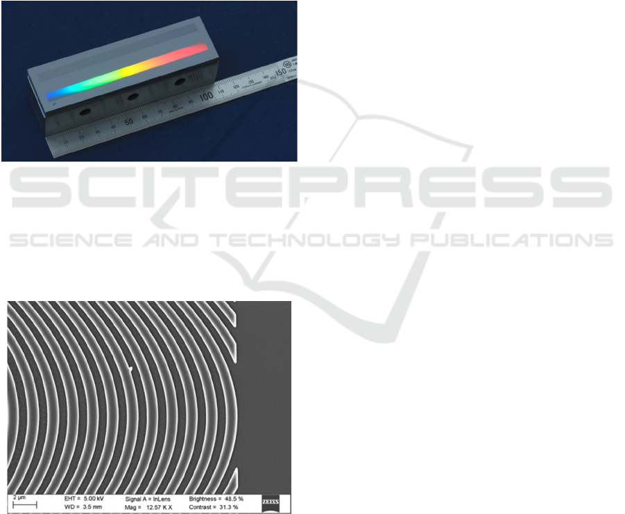
fabricated is shown in fig.4.
Figure 4: Aberration corrected diffraction grating grating a
The grating consists of gratings of three different line
density. 400 lp/mm (up); 800 lp/mm (down).
After the been fabricated, the structure of our
grating is carefully check using SEM, The SEM
images show that the sizes and positions of the
grating lines are the same as designed.
Figure 5: SEM image of the aberration corrected
diffraction grating grating. The curved grating lines are
designed to compensate the aberrations of a grating
monochromator.
4 CONCLUSIONS
We proposed a new diffraction grating, The
aberrations of a typical Czerny-Turner
monochromator are discussed in detail and the
grating design method is proposed in this work. The
relation between the wavefront and the position of
the grating line is analysed and the detailed design
method is discussed. A lamina type aberration
corrected reflective grating for soft X-ray is
fabricated using e-beam lithography, and the
detailed process is presented.
ACKNOWLEDGEMENTS
This work was funded by National Key Research
and Development Program of China (Grant
No.2017YFA0206002) and National Natural
Science Foundation of China-Chinese Academy of
Sciences Joint Fund for large-scale scientific facility
(Grant No.U1832217)
REFERENCES
Saitoh Y, Kimura H, Suzuki Y, Nakatani T, Matsushita T,
et al., 2000. Performance of a very high resolution soft
x-ray beamline BL25SU with a twin-helical undulator
at SPring-8, Rev. Sci. Instrum. 71, pp. 3254.
Chao W, Fischer P, Tyliszczak T, Rekawa S, Anderson E,
and Naulleau P, 2012 Real space soft x-ray imaging at
10 nm spatial resolution, Optics Express 20,9777
Noda H, Namioka T, and Seya M, 1974Geometric theory
of the grating, JOSA 64, 1031
Shafer A, Lawrence R. Megill, and Leann Droppleman,
1964 Optimization of the Czerny-Turner Spectrometer,
JOSA 54, 879
Reader J 1969 Optimizing Czerny-Turner Spectrographs:
A Comparison between Analytic Theory and Ray
Tracing JOSA 59, 1189
Mahajan V N, 1991. Aberration theory made simple, 43-
49
Zhao M, Zhu X L, Chen B Q, et al.2008 Design,
fabrication, and test of soft x-ray sinusoidal
transmission grating. Optical Engineering, 47, pp.
058001-058001-5
Fabrication of Aberration-corrected Diffraction Grating for Soft X-ray Grating Monochromator
113
