
HF RFID Reader for Mouse Identification - Study of
Magnetic Coupling between Multi-Antennas and a
Ferrite Transponder
C. Ripoll
1
, P. Poulichet
1
, E. Colin
2
, C. Maréchal
2
and A. Moretto
2
1
Université de Paris-Est, Esiee, Esycom
Cité Descartes, BP99, 93162 Noisy le Grand Cedex
2
Esigetel- Département de Télécommunications
1 rue du port de Valvins 77215 Avon-Fontainebleau
Abstract. This paper depicts an optimized RFID system operating at 13.56
MHz, used to recognize a mouse. When it passes near an antenna, the small
transponder (1x6 mm
2
) placed in its body communicates with the antenna. The
distance of communication is small (around 3 centimeters) and our objective
was to increase this distance. The transponder receives the signal from a coil
wound around a magnetic circuit. The characteristics of the ferrite are very
important for the communication. All the elements of the chain are taken into
account in ADS simulation and we determine the value of the minimum voltage
necessary for remote bias. Finite-element analysis is employed to extract the
values of the generated magnetic field. The paper shows how to correlate the
influent parameters to increase the communication distance. To improve this
reading rate, a novel differential receiving antenna has been designed allowing
an improved decoupling with the close transmitting antenna. An electrical
model of the different parts has been performed. This includes the tag, the
reader antennas and the coupling between them. These models have been
validated by measurements and used for the simulations of the complete
system.
1 Introduction
The principle used to identify a mouse is depicted on the figure 1. The biocompatible
transponder of 1 mm in diameter and 6 mm in length is introduced under the skin of
the mouse with a syringe. When the mouse passes in the vicinity of the transmitting
Antenna, the transponder receives the signal from the antenna. The amplitude of the
signal at 13.56 MHz has to be sufficient to supply the transponder and to transmit
coded signal. It reacts by sending a coded signal in order to identify the mouse.
The inductive coupling RFID (Radio Frequency Identification) systems operating
at 13.56 MHz are present nowadays in a large variety of applications, like access
control, mass transport, e-purse and secured ID cards. In a conventional system, they
are basically composed of one or more transponders dialoging with a base station by
means of a coupling through the close-field magnetic induction. The base station
produces a magnetic field that supplies power to the transponder, interrogates the tag
Ripoll C., Poulichet P., Colin E., Maréchal C. and Moretto A. (2008).
HF RFID Reader for Mouse Identification - Study of Magnetic Coupling between Multi-Antennas and a Ferrite Transponder.
In Proceedings of the 2nd International Workshop on RFID Technology - Concepts, Applications, Challenges, pages 32-42
DOI: 10.5220/0001728900320042
Copyright
c
SciTePress

and decodes the information received.
Fig. 1. Communication between the mouse and the Emitter antenna.
The two parts communicate in half-duplex mode: during the uplink, the base station
sends a request (ASK-modulated, 100% or 10% modulation index, depending on
radio interface type [1]) then it continues to transmit an unmodulated 13.56 MHz
carrier, which supplies power to the transponder IC; during the downlink, the
transponder responds by varying its load impedance, and thus modulating the carrier
sent by the base station (847.5 kHz OOK or BPSK-modulated subcarrier, depending
on radio interface type [1], switches between the impedance states), mechanism called
load modulation. The carrier will thus be modulated in amplitude (AM) and phase
(PM).
Current state-of-the-art in RF characterization of 13.56 MHz inductive coupling
identification systems only involves a basic check of the standard compliance [1], [2].
Although reference transponder circuits are used, no electrical parameter
measurement is performed.
In biomedical domain, where inductive links are used to deliver power and
exchange information with implanted stimulators, results have been published [3] –
[5], regarding the remote power supply in an inductive coupling system and its
variation when the coupling changes. Concerning the measurement methods, a
detailed analysis of coupled resonators is performed by Kajfez in [6], [7]. Majority of
proximity coupling applications concern the magnetic resonance imaging and a very
few for the RFID applications.
The RFID system can be modeled as a double-tuned transformer, whose primary
represents the base station and secondary the transponder. The transponder, often
called tag, is made out of an IC (integrated circuit) which capacitive input impedance
resonates with an antenna coil that collects the magnetic flux.
Proximity Radio Frequency Identification (RFID) systems physically relies on the
space evolution of their loop antennas mutual coupling, i.e. their shape, dimensions
and relative position. In order to optimize the antennas design, one needs to predict
the coupling evolution within the desired operating zone. Previous works in
biomedical domain focused on the coupling variation, mainly for circular loops.
2 System Description and Design Keypoints
A well-designed RFID system should ensure a safe functioning within a precise
geometric volume (i.e. voltage supply to the transponder IC and modulation depth
compliant with the manufacturer's specifications).
33

Three entities can be distinguished, whose interdependence should be understood: the
base station (i.e. antenna topology and detection threshold), the RF channel (i.e.
magnetic radiation pattern) and the transponder (i.e. IC and antenna).
When the transponder moves in the field of the base station, the induced voltage at the
IC input varies over a large range [4] (e.g. the magnetic field, varying between 1.5
and 7.5 A/m for systems compliant with [1], may induce a voltage of 5 to 35 V at the
IC). Moreover, the logic part of the IC needs a regulated voltage supply and a current
source, to avoid parasitic load modulation during its functioning. In these conditions,
a voltage-and-current regulation system varies the input capacitance and load
resistance of the IC. Thus, the overall functioning passes through a wide range of
states, given that the load mismatch represented by the transponder on the base station
antenna varies.
The aim of an RFID system used in biological experiments for identifying laboratory
mice or small animals is to be able to read the ID code in the largest volume zone
with the smallest transponder as possible to avoid stress and so unpredictable
behavior of the animal. For this reason, the transponder used here is an ultra small
transponder measuring only 1 by 6 mm encapsulated in a glass capsule. The system
operates in the world-wide ISM band of 13.56 MHz and not the classical 134 kHz
band used for animals, so as to reduce the size of the transponder antenna. With such
a tiny small transponder, it becomes compulsory to use a coil antenna wounded on a
ferrite rod to increase the induced voltage.
Before introducing the key points of this study, let us recall that the system operates
with the same minimal constraints as in any conventional proximity passive RFID
system. This means that we should take into account the remote biasing of the
transponder but as well the data exchange between the reader and the tag in a Listen
Before Talk protocol. In our case, to remote bias the transponder, first we must
radiate a high magnetic field, which means that a high current circulates through the
transmitting coil and second, the Q factor of the transponder should be optimized to
be rather high but not too high to avoid degrading the backscatter modulation bands
placed at +/- 848 kHz. These constraints call for a precise modeling of the transponder
parameters and particularly the Q factor. We note that in contrary to a smart card
reading system, we can here neglect the variations of the transfer function (i.e. band-
pass shape, resonance and Q-factor) as the coupling varies [3], [6].
Unfortunately, modeling such a tiny rod is theoretically unreliable due to the
difficulty to measure the magnetic losses, which are expressed by the µ
r
’’ of the
material. Consequently, the modeling will be based on the measurements of a
resonant transponder.
Another key point in this study was to avoid the coupling between transmitter and
receiver. In the transmitter path, very high voltage exists due to the matching circuits
and to the high current as we already mentioned. To reduce dramatically this problem,
we used a differential antenna on the receiver side. This design allows the perfect
cancellation of the carrier transmitted by the transmitting antenna when the coils are
ideally balanced. As a drawback for this geometrical configuration, we should
mention that the data exchange becomes impossible for a central position of the
mouse. This is of little importance because the mouse ID code has the opportunity to
be read at many points when it enters the bean-shaped reading zone. Obviously, the
coupling is finite and the topology of the receiver should take this into account.
34

This work is organized as follows. Section 3 presents the magnetic simulations of the
transmitting antenna. It shows the influence of the permeability of the transponder.
Section 4 describes the electrical modeling of the three parts (transponder, transmitter
and receiver). In Section 5, we perform electrical simulations of the complete system.
3 Magnetic Simulations of the Antennas
The figure 2 shows the shape of the transmitting antenna. It is realized with a round
PCB of diameter of 3 cm. The outside circular trace of each side of the PCB is used to
generate the transmitting magnetic field. The two inner spirals that constitute the
differential antenna used for the reception are connected together and one point is
connected to the ground.
Fig. 2. Shape of the transmitting antenna and differential antenna.
The simulation is operating using 2 dimensions FEM (Finite Element Modeling) with
Ansys [8]. Figure 3 represents the model used for FEM. It represent a cut along the
axis A-A of the figure 2. The permeability µ
r
’ (120 for ferrite of the transponder), the
resistivity σ of the materials and the current in the conductors are taken into account
in order to determine the magnetic field in magneto dynamic simulations.
Fig. 3. Geometry for the FEM.
A measurement of the inductance of the transmitting antenna shows that the spiral
inductance has no effect on the magnetic field so they are not taken into account in
the simulation.
Figure 4 shows the module of the magnetic induction (B) determined in axis-
symmetric simulation. The high permeability of the transponder concentrates the
magnetic field generated by the current in the transmitting antenna. This permeability
is a key point design because a high value increases the distance of reception.
However, it is difficult to obtain a high value at 13.6 MHz without loss.
35
We determine the magnetic induction (B) at distances d of 0.5 cm, 1 cm, 2cm and 3
cm. The curve is represented on the figure 5.
0 0.005 0.01 0.015 0.02 0.025 0.03
0
1
2
x 10
-4
distance x (m)
B (T)
Induction B(T) obtained by FEM as a function of distance
0.5 c m
1 cm
2 cm
3 cm
radius
Fig. 4. B values near the transmitting
antenna.
Fig. 5. Magnetic induction B (T) with respec
t
to distance d on a parallel line for x=0.
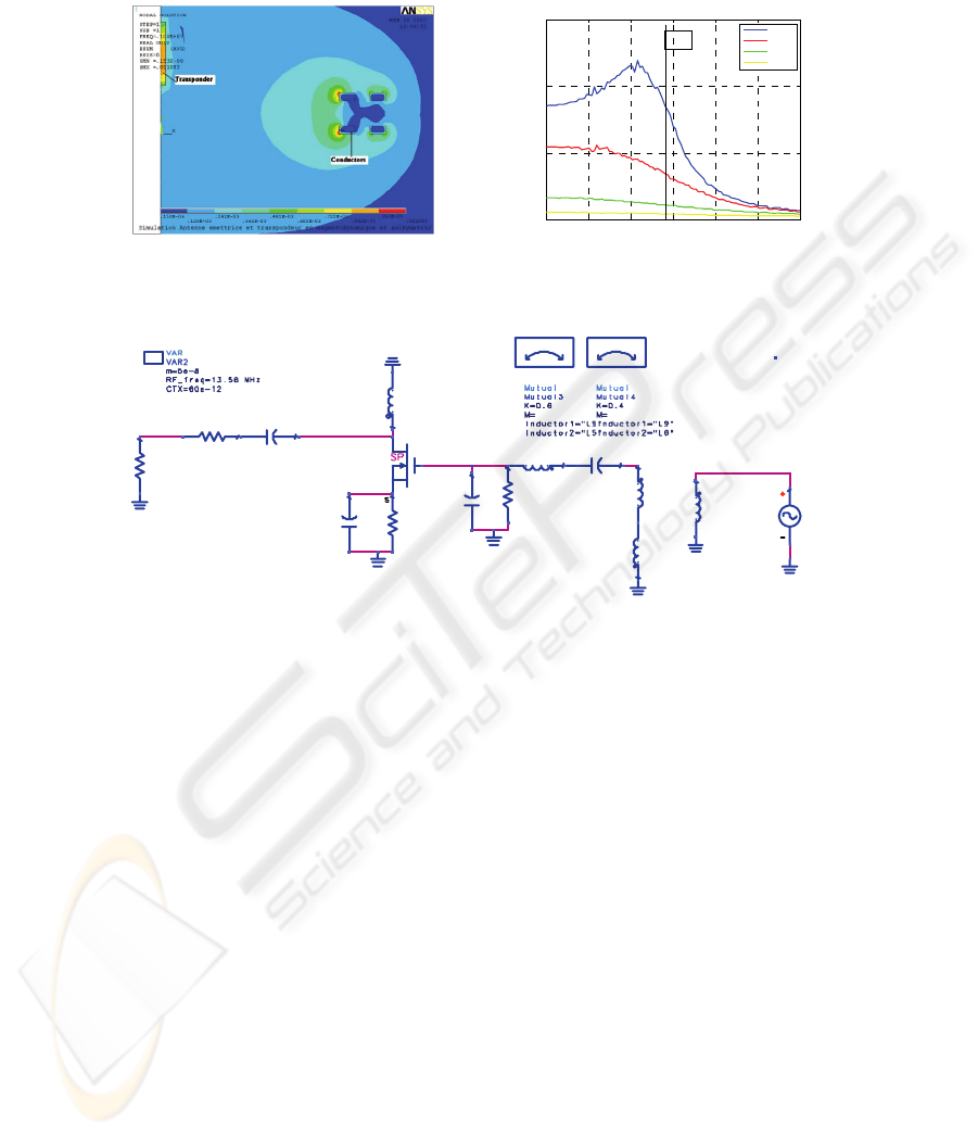
VGMOS
Vout VDMOS
Vrx
Eqn
Var
MU T I N D MUT I ND
L
L6
R=1
L=1 uH
V_AC
SRC7
Freq=freq
Vac=polar(6,0) V
L
L9
R=0.3
L=390 nH
R
R11
R=1 MOhm
C
C26
C=22 pF
R
R10
R=820 Ohm
C
C25
C=100 nF
R
R9
R=120 Ohm
L
L8
R=37 Ohm
L=22 uH
sp_sms_BF998_1_19920901
SNP1
Frequency ="{0.05 - 2.00} GHz"
Bias="Mosf et: Vds=5V Vg2s=3.5V Id=10mA"
C
C24
C=12 pF
R
R8
R=5k Ohm
L
L7
R=
L=1 uH
C
C23
C=100 pF
L
L5
R=1
L=1 uH
Fig. 6. Differential receiver schematic.
When the distance d increases, the magnetic induction B is reduced. When the
distance x is higher than the radius of the transmitting antenna, the induction B is
reduced.
4 Characterization Receiver, Transmitter and Transponder
To be able to optimize the whole system, we have to study the individual components.
4.1 Measurements of the Parameters of the Receiver
The electrical circuit of the receiver is shown in figure 6. Its transfer function is
simulated by injecting a signal through a non resonant generator inductively coupled
(L9 transmitting antenna) to the two coils representing the differential spiral antennas
in figure 2 and L5-L6 in figure 6. The received signal is transmitted through a band-
36
pass (C23-L7-C24) to the MOS transistor used to amplify the signal. The circuit is
designed so that its transfer function is centered on 14.4 MHz frequency that
corresponds to one of the symmetric backscattered bands around the 13.56 MHz
carrier. We have to mention that the parallel resistance R8 allows the setting of the
bandwidth, so is influent for the filtering of the carrier residual and will have an
impact on the distortion of the modulated bandwidth.
4.2 Measurements of the Parameters of the Transmitter
The schematic of the transmitter is represented in figure 5. M2 is a MOS transistor
operating in a low loss switching mode. It generates a high current circulating in the
transmitting antenna L1. C13, C22//C21//C12 and L1 constitute a parallel resonant
circuit. C21 or Ctx is a variable capacitor adjusted to facilitate the remote bias of the
transponder. Frequency analysis has to be taken into account as a first step to adjust
the resonant frequency. Furthermore, the shape of the voltage across the transmitting
antenna has to respect a standard waveform (see 4.2.2).
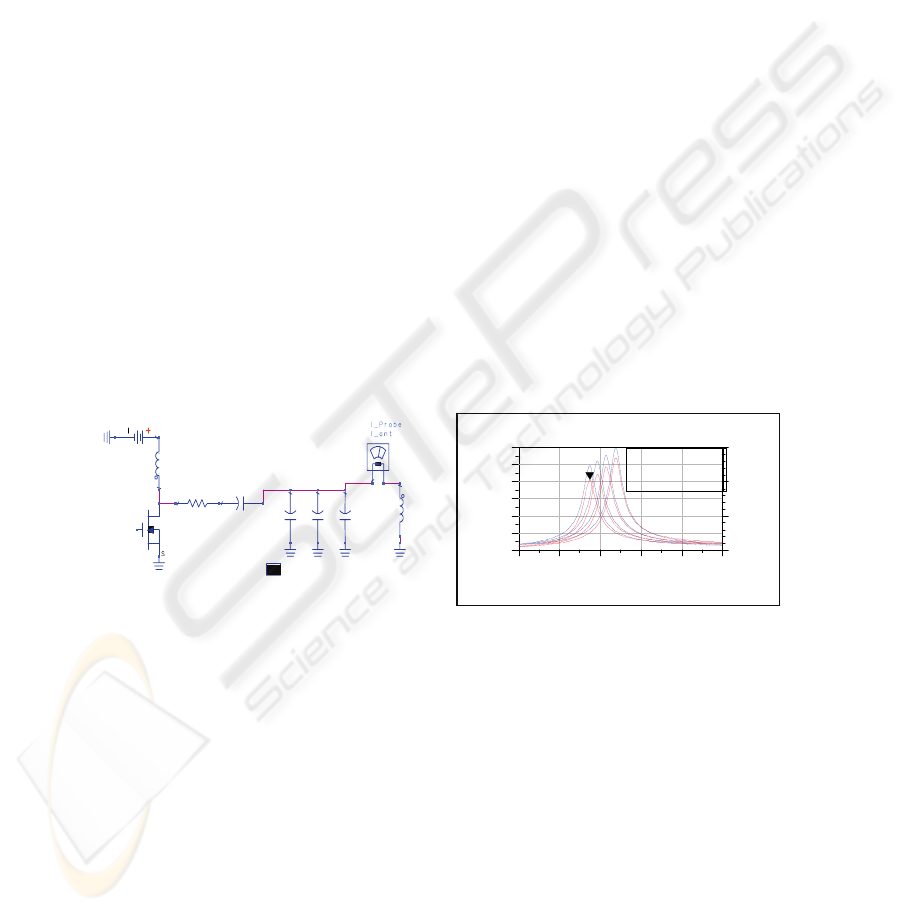
4.2.1 Frequency Analysis
The transfer function is simulated with a sinusoidal excitation, then we derive for
which value of Ctx, we obtain a maximized current (I_Probe) in the transmitting coil.
The resonant frequency has to be set up at 13.56 MHz to induce the necessary voltage
at the input of the IC tag. This is achieved through the use of the Ctx parallel
capacitor.
Self 3.3uH / 0.5 Ohm mesure
Vtx
V_DC
SRC4
Vdc=12 V
VAR
VAR5
RF_freq=13.56 MHz
CTX=70e-12
Eqn
Var
R
R9
R=0 Ohm
L
L4
R=0. 5
L=3.3 uH
L
L1
R=1.3
L=390 nH
C
C12
C=47 pF
C
C21
C=CTX
C
C22
C=150 pF
ap_nms_IRFD020_19930601
M2
C
C13
C=100 pF
Fig. 7. Transmitter schematic. Fig. 8. Variation of the Transmitter transfe
r
function with variable Ctx values.
As shown in figure 8, the transfer function is a band-pass type which quality
coefficient has to be around 30 to avoid degradation of the 200 kHz modulation
bandwidth around the carrier.
Figure 8 represents the shift of the central frequency as a function of Ctx. We note
that it is preferable for the transmitter not to operate at 13.56 MHz (Ctx=70pF) but
rather near this frequency. For example, we obtained best results for a value of 14.4
MHz (Ctx=35pF).
m2
freq=
mag(Vtx)=40.897
CTX=6.000000E-11
13.50MHz
12 14 16 1810 20
10
20
30
40
50
0
60
0.5
1.0
0.0
1.5
freq, MHz
mag(I_ant.i)
mag(Vtx)
m2
m2
freq=
mag(Vtx)=40.897
CTX=6.000000E-11
13.50MHz
37
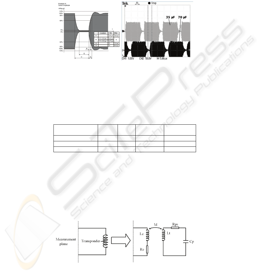
4.2.2 Temporal Analysis
We should consider the time domain response because, to operate properly, any
Mifare UltraLight IC at the tag should be able to detect the presence of a pause in the
transmitted signal. This means that the matching / filter circuit should respect the
waveform shown in figure 9.
Fig. 9. Standard waveform and Measured voltages at and near resonance (Ctx=35pF and 70
pF).
The table 1 shows that times t2 and t4 depend largely of the value of Ctx. In the case
of 35 pF, t2 is near of the minimal value and with 70 pF, t2 is too low. For Ctx = 70
pF, the distance of detection of the transponder is likely to be too small.
Table 1. Comparison between ISO14443 and simulated results for transmitter operating at and
near resonance.
t1=2 uS Min Max Ctx=35 pF
(near)
Ctx=70 pF
(at resonance)
t2 (5% decay time) 0.7 uS t1 0.6 us 0.5 us
t3 (90% rise time) 0 1.5 uS 0.33 uS 1.22 uS
t4 (60% rise time) 0 0.4 uS 0.19 uS 0.51 uS
4.3 Measurements of the Parameters of the Transponder
Because the parameters have to be extracted in a non destructive test, we use a
contactless methodology. The transponder was placed in a test primary coil shown in
figure 10. The resistance Re and inductance Le of this coil have been characterized
with an impedance analyser. Then the mutual coefficient between this primary coil
and a transponder without its IC has been extracted by measurement of the induced
voltage at the open transponder coil.
Fig. 10. Set-up to measure the parameters of the transponder.
38
The equation giving the impedance at the primary coil is:
ωω
ω
ω
ppstt
ee
jCRRjL
M
RjLZp
/1
22
+++
++=
(1)
Rt, Lt: Series resistance and inductance of the transponder coil without ferrite.
Lt: Inductance of the transponder coil with ferrite.
Rps: Series resistance due to magnetic losses.
Cp: input capacitance of the IC.
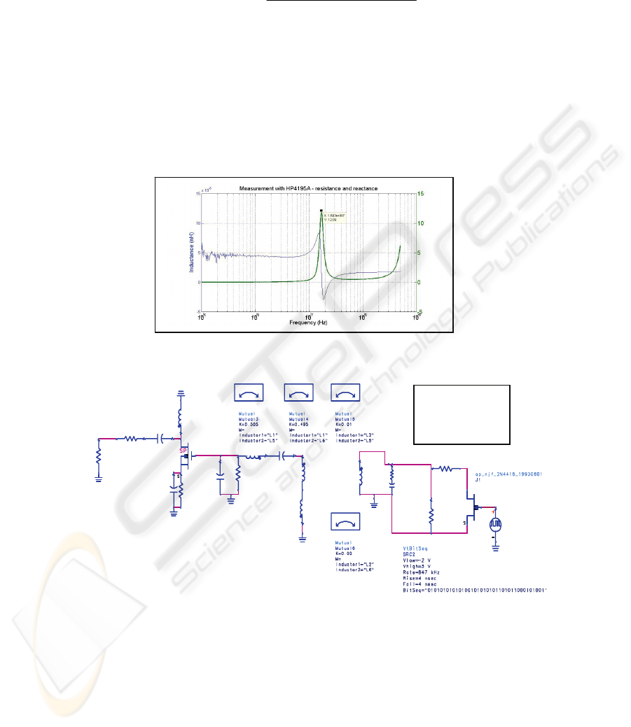
By measuring the resonance frequency, input resistance and reactance at the primary
coil, one can extract the frequency at which denominator cancels. So, because the
input capacitance is known, the value of secondary inductance and resistance are
extracted.
Fig. 11. Measurement of input impedance at primary coil.
Vdata
Vb
Vi n_rx VDMOS
VGMOS
Vrx
L
L2
R=8
L=2.65 uH
t
R
R6
R=1 kOh m
SRC
SRC5
C=50 pF
R=1 Ohm
R
R7
R=1.5 kOhm
MUTI ND
MUTI ND
R
R2 2
R=5 0 Ohm
R
R1 2
R=820 Ohm
C
C2 6
C=2 2 p F
C
C2 5
C=100 nF
R
R1 0
R=500 Ohm
C
C2 4
C=7 0 pF
L
L7
R=0 . 5
L=1 uH
MUTINDMUTIND
L
L5
R= 1
L=1 uH
L
L6
R=1
L=1 uH
sp_sms_BF998_1_19920901
SNP1
Frequency="{0.05 - 2.00} GHz"
Bias="Mosfet: Vds=5V Vg2s=3.5V Id=10mA"
R
R1 3
R=120 Ohm
L
L8
R=37 Ohm
L=22 uH
C
C2 3
C=100 pF
Fig. 12. Complete system (Transmitter not represented but all mutual inductances are present).
5 Characterization of the Complete System
Now we can proceed to the simulation of the complete system. All the individual
elements have been optimized according to known criteria as for example to
k(TX-TPR)=2.5%
k1(TPR-RX)=1%
k2(TPR-RX)=2%
k1(TX-RX)=50.5%
k2(TX-RX)=49.5%
39
maximize the radiated H field or to center the RX filter onto one backscattered side
band. The position of the mouse when crossing the reading volume is taken into
account by considering variable coupling coefficients between the transponder TPR
and receiver RX. As shown in figure 5, the magnetic induction received by the
transponder changes and the coupling coefficient follows.
In figure 12, the complete system is represented (note that transmitter does not appear
for clarity) with all the mutual coefficients between transmitter TX, receiver RX and
transponder TPR.
The coupling coefficients k (TX-RX) between TX and RX are made variable. The
tests are performed for weak coupling (transponder in the farthest zone) and for a non
ideal coupling (zero coupling) between transmitter antenna and differential receiver
antennas:
The differential antenna system has been modelized by two coils in series which
induced currents are inverted according to the reference dot (simulates the inverted
windings of the spirals). In the case of ideal coupling between Tx and Rx, the induced
voltages in the spiral antennas is null. To account for the non ideal case, we consider
non equal mutual coefficients.
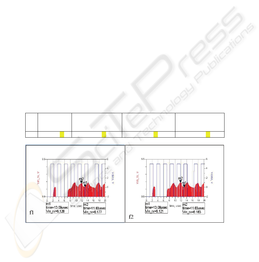
We note important results in table 2. Even in the case where there is no coupling
between the transponder and the receiver (f1), a modulated signal is present as shown
in figure 14. Actually, it comes from the transmitter which is coupled to the
transponder. So, it means that even in the case of null coupling, because the
transmitter and the receiver antennas cannot be perfectly uncoupled, data exist in the
receiver.
Table 2. Received modulated voltage with different TPR to RX coupling coefficients.
Vrx
No coupling
to TPR-RX
With equal coupling
k1=0.01 k2=0.01
With unequal coupling
k1=0.01
k2=0.02
With no Tx-Rx
coupling
k1=0.02 k2=0.01
60mV f1 60mV f2 62mV f3 140mV f4
Fig. 13. Waveforms at the receiver for 4 case studies:
f1: with no coupling between Tpr-Rx and coupling between Tx-Rx.
f2: with equal coupling between Tpr-Rx and coupling between Tx-Rx.
40
Fig. 14. Waveforms at the receiver for 4 case studies (cont.):
f3: with unequal coupling between Tpr-Rx and coupling between Tx-Rx.
f4: with unequal coupling between Tpr-Rx and no coupling between Tx-Rx.
We can even add that this is the main coupling mechanism because in the case of
coupling between transponder and receiver (f2, f3), the modulation voltages are of the
same order. Besides, this extra coupling has the effect of multipath summation in
propagation. It means that we can distort the shape of the received data. This is
confirmed by the last case (f4) in figure 14 where we nullified the coupling between
transmitting and receiving antennas (ideal operation mode). We observe that
amplitude is more than double and much closer to the generated square waveform
from the transponder.
6 Conclusions
To optimize an RFID reader magnetically coupled to a tiny ferrite transponder,
compromises have to be made. On the transmitter side, the matching circuit between
the switching MOS transistor and the coil antenna is optimum and should be tuned at
13.56 MHz to maximize the radiated H-field so as to maximize the transponder
induced voltage. This matching circuit should be tuned slightly above 13.56 MHz if
waveform of the modulated signal (pause) is to be fit with the ISO14443
recommendation. On the receiver side, the matching circuit between the differential
coil antennas and the Low Noise Amplifier is to be centered on the side band (13.56
MHz plus the subcarrier frequency = 14.4 MHz) with a bandwidth that should
preserve the integrity of the modulation data. As for the transponder, it is a key
element and the ferrite itself should be chosen with great care due to the detrimental
effect of too high magnetic losses. In the extracted model, we found 8 Ohms for the
equivalent resistance which is the primary factor to determine the Q, here 10. This
quality factor means a bandwidth of around 1.5 MHz, which is necessary to preserve
a sufficient bandwidth to receive and send the data from and to the transmitter. Due to
the shape of the rod, the effective permeability is much less than the relative
permeability. We computed and measured an effective µ
r
’ of 14 for a relative µ
r
’of
120. To determine the induced voltage, magnetic simulations have been performed so
as to calculate the B field at any point in the reading volume.
41

A differential receiving antenna to avoid the strong voltage which occurs in classical
HF systems has been designed. We managed to obtain a reduced coupling with safe
voltage values. We noticed as well that this imperfect coupling means an intermediate
path for the data to couple from the transponder to the receiver. In consequence, the
reading volume is larger than foreseen, because there is no dead zone but as a
drawback, the data may be distorted. To reduce the Tx-Rx coupling, the Tx antenna is
built with two coils, one on each side of the board to insure the symmetry with the
spiral antennas.
In conclusion, an HF reader has been simulated, built and optimized to reach a
reading distance of about 3 cm for an ultra-small ferrite transponder injected under the
skin of the mouse.
References
1. "Identification cards - Contact less integrated circuit(s) cards - proximity cards", ISO / IEC
14443 – 2 international standards, Part 2 "Radio frequency power and signal interface".
2. "Identification cards – test methods", ISO / IEC 10373-6 international standard, Part 6
"proximity cards".
3. N. Chaimanonart, K. R. Olszens, M.D. Zimmerman, W.H. Ko, D.J. Young, “Implantable
RF Power Converter for Small Animal In Vivo Biological Monitoring”
Engineering in Medicine and Biology Society, 2005. IEEE-EMBS 2005. 27th Annual
International Conference, 2005 pp 5194 – 5197.
4. M. Soma, D. C. Galbraith, R. L. White, "Radio-frequency coils in implantable devices:
misalignment analysis and design procedure", IEEE Trans. on biomedical engineering, vol.
BME-34, No. 4, pp 276-282, April 1987.
5. C. M. Zierhofer, E. S. Hochmair, "Geometric approach for coupling enhancement of
magnetically coupled coils", IEEE Trans. on biomedical engineering, vol. 43, No. 7, pp
708-714, July 1996.
6. D. Kajfez, "Dual resonance" IEEE Proceedings, vol. 135, Pt. H, No 2, pp 141-144, April
1988.
7. D. Kajfez, "Q-factor measurement with network analyzer", IEEE Transactions on
microwave theory and techniques, vol. MTT-32, No. 7, pp 666-670, July 1984.
8. Ansys Software. Magneto-dynamic simulation. www.ansys.com
42
