
IN-SITU MEASUREMENT AND VISUALIZATION
OF ELECTROMAGNETIC FIELDS
Satoshi Yagitani, Mitsunori Ozaki
Institute of Science and Engineering, Kanazawa University, Kakuma-machi, Kanazawa, Japan
yagitani@is.t.kanazawa-u.ac.jp, ozaki@is.t.kanazawa-u.ac.jp
Yoshiyuki Yoshimura, Hirokazu Sugiura
Industrial Research Institute of Ishikawa, 2-1 Kuratsuki, Kanazawa, Japan
yyoshi@irii.jp, h-sugiura@irii.jp
Keywords: Electromagnetic fields, Radio-frequency fields, Measurement, Visualization, EMC, Absorber.
Abstract: In-situ monitoring of electromagnetic field distributions is useful for localizing and identifying EM noise
sources, as well as for evaluating actual antenna characteristics. A couple of new techniques developed for
in-situ measurement and visualization of electromagnetic fields are reported. At first, visualization of EM
field distributions measured by a freehand scanning sensor on a live video image is described. Secondly,
imaging of 2-d RF field distributions incident on a metamaterial absorber is explained. Then, in-situ
visualization techniques for EM vectors and RF polarizations are discussed. Such techniques are expected
to be quite useful for measuring EM field distributions in various scenarios in the fields of EMC, antennas
and propagation.
1 INTRODUCTION
In-situ measurement of the actual spatial
distributions of electromagnetic (EM) field is useful
for localizing and identifying EM noise sources in
electric or electronic equipment under actual
operating conditions, as well as for evaluating the
performance of antennas in wireless communication
devices used in real environments. Conventionally,
the spatial distributions of the EM field have been
measured by scanning the plane/volume of interest
with a sensor or sensor array. So far there have been
proposed and developed a wide variety of mapping
and cartography systems of EM distributions from
the viewpoint of EMC/EMI. For radio-frequency
(RF) fields from tens of MHz up to tens of GHz,
various kinds of sensor-scanning systems have been
developed to measure RF emissions from electronic
devices and systems, individual PCBs, and even
onboard VLSI chips. In these systems, for example,
an electric field probe (Dutta et al., 1999), a
magnetic loop probe (Haelvoet et al, 1996), a
magnetic sensor array (Yamaguchi et al., 1999), and
an electromagnetic field probe (Kazama and Arai,
2002) have been used with mechanically-scanning
systems (Baudry et al., 2007), which have measured
and visualized RF near-field distributions. A 2-d
dense array of thousands of loop sensors for near-
field distribution imaging (without the need for
scanning) has also been available (Fan, 2009). The
near-field distributions have been used to identify
radiated emission sources (Laurin et al., 2001) and
to predict far-field noise radiation (Shi et al., 2004).
Another study has measured Fresnel near-field
distributions to holographically localize RF leakage
points for example from a shielded door (Kitayoshi
and Sawaya, 1999) and from the surface of
spacecraft (Chen et al., 2012).
It is noted that for dc to low-frequency magnetic
field application, there have been independently
developed the imaging systems such as
“magnetovision” with scanning 1d and 2d
magnetoresistive (MR) sensor arrays, to obtain
principally dc magnetic field images, for example
for investigation of magnetized materials (Tumanski
and Liszka, 2002; Tumanski and Baranowski, 2006).
Another unique RF field imaging technique has
been proposed which employs an infrared (IR)
21
Yagitani S., Ozaki M., Yoshimura Y. and Sugiura H.
IN-SITU MEASUREMENT AND VISUALIZATION OF ELECTROMAGNETIC FIELDS.
DOI: 10.5220/0004784700210029
In Proceedings of the Second International Conference on Telecommunications and Remote Sensing (ICTRS 2013), pages 21-29
ISBN: 978-989-8565-57-0
Copyright
c
2013 by SCITEPRESS – Science and Technology Publications, Lda. All rights reserved
thermogram (Norgard and Musselman, 2004). An
RF field impinging on a lossy screen is absorbed and
creates a temperature rise there corresponding to a
map of absorbed power distribution, which is taken
by an IR camera. A “live electro-optic (EO)
imaging” system has employed an ultra-parallel
photonic heterodyne technique to take a video image
of electric near-field distribution applied on an EO
crystal plate at microwave frequencies (Sasagawa et
al., 2007). The electric fields more than tens of GHz
were down-converted and lively displayed at 30
frames/second as a 2d image with 100x100 pixels.
Generally these techniques give accurate
cartographic mapping and images of EM fields, but
require specific sensor scanning devices or imaging
systems. In constrast, the authors’ group have been
developing compact in-situ measurement and
visualization techniques for EM fields, which could
be used to capture an intuitive view of EM
distributions existing in actual environments. In this
paper a couple of developed techniques to measure
and visualize EM field distributions are reported.
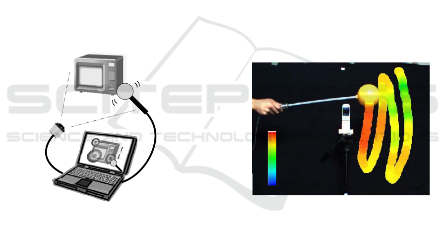
Figure 1: EM field distribution imager.
2 EM FIELD MEASUREMENT
AND VISUALIZATION ON A
VIDEO IMAGE
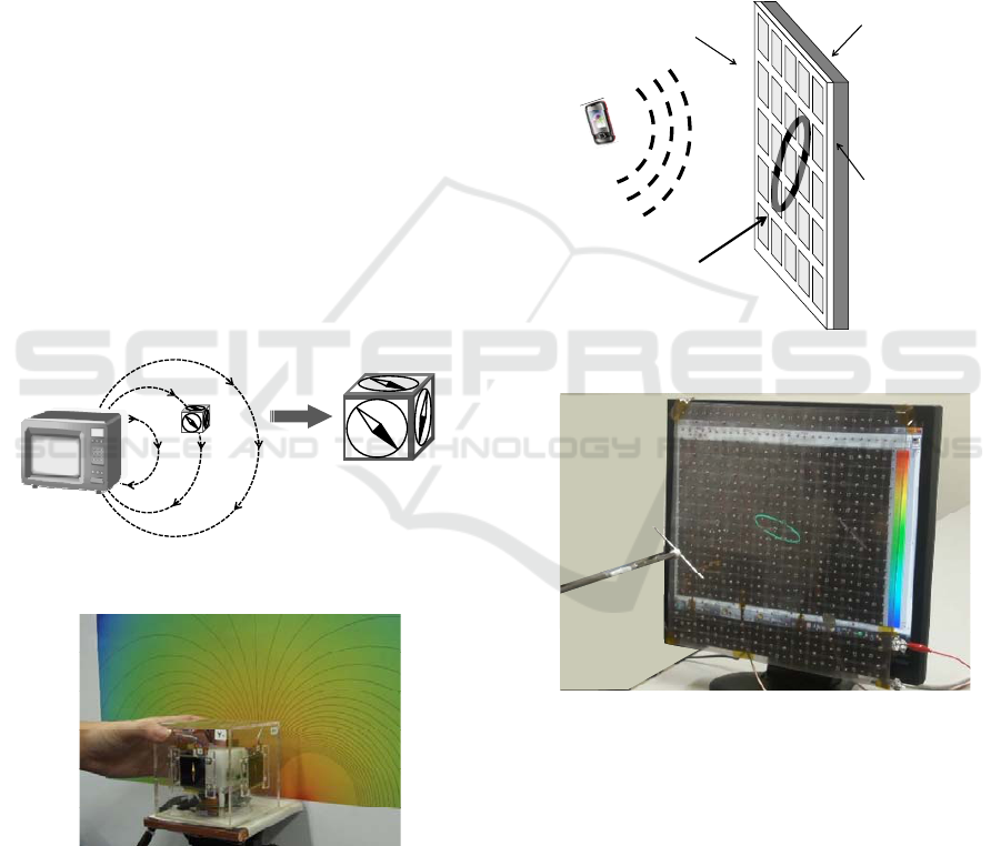
2.1 EM Field Distribution Imager
The “EM field distribution imager” illustrated in
Figure 1 measures and visualizes in-situ EM field
distributions on a live video image of the real world.
The image of an EM sensor is taken by a single
video camera. Image processing is applied on a PC
and the location of the sensor is identified on each
frame of the video image, where the sensor location
is painted with the color representing the EM field
intensity actually measured by the sensor itself. By
freely scanning the sensor by hand, the image of the
in-situ field distribution is gradually showing up
along the sensor trajectory as a color map on the
video image. Figure 2 shows an example of the RF
field (1.9 GHz) visualization around a mobile phone.
A sleeve dipole antenna was put inside a yellow
acrylic spherical cover of 10 cm diameter. A video
camera was placed 1 m away from the cell phone
put on a tripod in an office room. Here the 3d
location of the sensor was identified by extracting
the yellow circle on the image, the center and size of
which gave information on the sensor’s lateral and
depth location relative to the camera. Along the
freely scanned trajectory an intensity map of the RF
filed was created, which exhibited a standing-wave
pattern possibly caused by reflection at the wall or
floor. With this system one can scan the space of
interest while watching the video image, to obtain an
intuitive view of EM field distribution, in every
situation wherever the video camera and the sensor
can be carried in.
Figure 2: RF field imaging around a mobile phone.
This kind of freehand-scanning method has been
developed also by other researchers, based on
magnetic tracking, optical tracking and IR tracking,
for the investigation of the low-frequency magnetic
noise emitted from electrical appliance (Sato et al.,
2010; Sato et al., 2012).
2.2 Magnetic Field Vector Imaging and
Source Current Estimation
Even with a single video camera, this system can
determine the sensor’s 3d orientation in addition to
its 3d location, by putting a specific marking on the
spherical sensor cover. One way is to paint three
marks with different colors indicating the three axial
directions of the internal sensor, which are
EM sensor
Video camera
PC
Sensor
-60
-30
[dB]
Second International Conference on Telecommunications and Remote Sensing
22
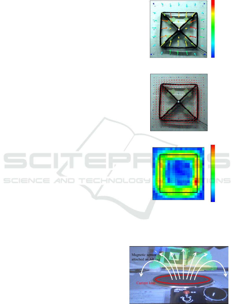
recognized on the video image to calculate the
sensor orientation. This makes it possible to
measure EM vector directions when we use an EM
vector sensor. Figure 3 (a) shows an example of the
magnetic field vectors measured and visualized
around a 45x45-cm square loop antenna (10 kHz, 63
mA-Turns), where the 2d projection of the measured
3d vectors are plotted with length and color
indicating the field intensity. Though not shown
here a tri-axial magnetic search-coil sensor was
used; three 10-cm-long uni-axial sensors were
placed orthogonally with each other, covered by a
15-cm acrylic sphere. A perpendicular plane 1 m
away from the camera (and 9 cm in front of the loop
plane) was manually scanned by the sensor.
Measurement was done at 7x7=49 points on a 60x60
cm area. Compared with theoretically calculated
values, the measured errors in intensity and vector
direction of the magnetic field were less than 10%
and 10 degrees, respectively. These errors were
caused by the errors in location (3 cm) and in
orientation (a few degrees) of the sensor which was
identified on a 640x480-pixel video image.
From the measured magnetic field vectors the
source current distributions were estimated by the
GVSPM method on the plane including the loop
source (Yagitani et al., 2007). Figures 3 (b) and (c)
plot the estimated source current vectors and
amplitudes on the loop plane. The estimated current
vectors are visualized on the real image of the loop
source, where the estimated current is practically
reconstructed along the actual square route of the
loop current. Thus, the free-scanning system is
expected to contribute not only to imaging of EM
field distributions but also estimating their sources.
2.3 EM Imaging by Smartphone and
Tablet PC
The measurement and visualization technique has
also been implemented onto a smartphone and tablet
PC. Figure 4 shows an example of a low frequency
(60 Hz) magnetic field distribution around an
electric cooker, which was measured by a magnetic
sensor with an augmented reality (AR) tag attached,
and visualized on a smartphone screen. With these
up-to-date devices, built-in cameras are used to take
a video image, while they can easily communicate
with the sensors through wireless links.
Furthermore an open-source AR software makes it
easy to implement the sensor identification
capability on the video image in a smartphone/tablet
app.
Figure 3: Low-frequency magnetic field vectors and
estimated current distribution: (a) measured magnetic field
vector distribution, (b) estimated current vectors, (c)
estimated current amplitude distribution.
Figure 4: Low-frequency magnetic fields from an electric
cooker, measured by a magnetic sensor with an AR tag
attached, and visualized on a smartphone screen.
(b)
-30 0 30
-30
0
30
x [cm]
0.13
0.00
Magnetic field [A/m]
-30 0 30
-30
0
30
x [cm]
y [cm]
(a)
25
0
Estimated current [mA-Turns]
(c)
-30 0 30
-30
0
30
x [cm]
y [cm]
In-Situ Measurement and Visualization of Electromagnetic Fields
23
3 RF FIELD DISTRIBUTION
IMAGER USING
METAMATERIAL ABSORBER
3.1 Metamaterial Absorber
It has been proposed that a metamaterial absorber
could be used for monitoring 2d power distributions
of a radio-frequency (RF) wave incident on the
absorber surface (Yagitani et al., 2011a). The
metamaterial absorber was designed by employing a
mushroom-type electromagnetic band-gap (EBG)
structure used as a high-impedance surface
(alternatively called an artificial magnetic
conductor). As shown in Figure 5 (a), a 2d matrix of
dense square metal patches formed on a dielectric
substrate were connected to the ground plane
through vias. Lumped resistors interconnecting the
square patches were placed on the surface to absorb
the incident wave (Gao et al., 2005). A simple
equivalent circuit based on the transmission line
model for the absorber is shown in Figure 5 (b); the
capacitance C is formed between the adjacent
patches whereas the inductance L comes from the
wave propagation (transmission line) inside the
substrate (Luukkonen et al., 2009). At the resonance
frequency the LC impedance becomes infinite so
that the surface resistance R absorbs the incident
wave if R is matched with the free space wave
impedance, 377 , for normal incidence. Figure 5
(c) shows the reflection and absorption
characteristics; the maximum absorption (minimum
reflection) occurs at the resonance frequency. Since
L and C are determined by the metamaterial
structure, varactor diodes were inserted parallel to
the resistors to make the resonance (absorption)
frequency tunable (Mias and Yap, 2007).
3.2 RF Power Distribution
Measurement
The configuration of this kind of metamaterial
absorber makes it possible to directly measure the
amounts of power absorbed (or consumed) by the
individual lumped resistors. As in Figure 6, an RF
power detector can be attached to each resistor and
measure the absorbed power. A 2d array of power
detectors attached to the lumped resistors are used to
capture the 2d image of the RF power incident and
absorbed on the surface. The amount of power
absorbed by each resistor is dependent on the
incident polarization; the incoming RF waves with
the electric field polarized in the x- and y-directions
are absorbed by the resistors connecting the adjacent
patches in the x- and y-directions, respectively. In
either case, the power absorbed by each resistor is
considered to be the Poynting flux of the incident
wave multiplied by the area of one unit cell. Thus,
the information on the incident polarization is
obtained by the power detectors individually
attached to the x- and y-resistors.
Figure 5: A metamaterial absorber: (a) basic structure, (b)
equivalent circuit, and (c) reflection and absorption
characteristics.
Figure 6: Measurement of absorbed RF power
A metamaterial absorber was designed and
fabricated which was made tunable between 700
MHz and 2.7 GHz (Yagitani et al., 2011a). A 33x33
array of square unit cell were formed on an FR-4
substrate of 347 mm square and 1.6 mm thick. The
size of each patch was 10 mm and the gap between
the adjacent patches was 0.5 mm. Lumped resistors
(620 ) and RF varactor diodes (Infineon BB833)
C
L
R
x
y
(a)
(b)
Resistor
Substrate
GND
Patch
Via
‐40
‐30
‐20
‐10
0
7.000E+088.000E+089.000E+081.000E+091.100E+091.200E+ 09 1.300E+09
Frequency
[dB]
Reflection
Absorption
-40
0
-20
f
0
(c)
GND
Surface
RR
Incident RF wave
Second International Conference on Telecommunications and Remote Sensing
24

were inserted in parallel between the patches. The
equivalent circuit model of the absorber is given in
Figure 7, where C
D
, L
D
and R
D
are the stray
capacitance, stray inductance and resistance of a
varactor diode, respectively, and R
loss
represents the
dielectric loss of the substrate. Detailed analysis of
such a circuit was made to reveal that even a small
varactor resistance (a few Ohms) is translated to a
larger surface resistance which severely degrades the
absorption performance especially at lower
frequencies (Yagitani et al., 2011b). The
performance of the absorber is shown in Figure 8
(with data taken from Yagitani et al., 2011a), where
a black solid line, a gray line and a broken line
represent the measured profile, the profiles obtained
by equivalent-circuit analysis and EM simulation
(CST MW-STUDIO), respectively. These profiles
practically agree with each other. The symbols A, B,
C and D correspond to the varactor capacitances of
3.35 pF, 1.72 pF, 1.09 pF and 0.72 pF, respectively.
Here the lumped resistors had been chosen as 620
so that the maximum absorption was obtained at
2.62 GHz.
Figure 7: Equivalent circuit model of the fabricated
metamaterial absorber.
Figure 8: Absorption performance of the fabricated
metamaterial absorber (data from Yagitani et al., 2011a).
Figure 9: RF power distribution imager.
Using the fabricated absorber an RF power
imager was developed, as schematically illustrated
in Figure 9. The RF power distribution incident on
the surface was detected by an array of power
detectors attached on the backside of the absorber.
An array of 64 power detectors were arranged in a
8x8 matrix to measure the x-polarization, whereas
another array of 64 detectors were placed for the y-
polarization. A logarithmic power detector (Analog
Devides, ADL5513) was used, which measures the
power in the range from -70 dBm to +10 dBm
between 1 MHz and 4 GHz. The detected RF power
distribution was A/D converted, transferred to a PC
and displayed as a 2d color map at 30 images/second.
With this system, RF power distributions
radiated from a standard dipole antenna were
measured in the experimental setup shown in Figure
10 (a). A horizontally polarized radio wave (0 dBm)
at 2.2 GHz was transmitted from the antenna placed
at a distance d from the absorber. Figure 10 (b)
plots the measured power distribution of horizontal
polarization at d = 10 cm. An elliptic power
distribution corresponding to the directivity of the
horizontal dipole was captured. The power
distributions along the x- and y-axes are compared
with the theoretical values in Figure 10 (c), which
were calculated according to the previous work
(Yagitani et al., 2011a). Here each power detector
had been calibrated by an almost far-field and plane-
wave pattern, created by the transmitting antenna
placed at d = 80 cm. For distances of d = 30 cm and
50 cm, the measured profiles practically agree with
the theoretical curves. At a distance of 10 cm,
however, the measured profiles became weaker than
the theoretical ones. This would be caused by that at
this short distance the radiated field did not
completely become a far-field so that impedance
mismatch caused the reflection from the absorber
surface. More rigorous treatment for near-field
spherical wave incidence is needed to quantitatively
discuss the accuracy of power distributions at such a
short distance.
R
C
L
0
= 377
Incident wave
C
D
L
D
R
loss
R
D
-35
-30
-25
-20
-15
-10
-5
0
5
123
S
11
Magnitude [dB]
Frequency [GHz]
1 2 3
Frequency [GHz]
S
11
Magnitude [dB]
5
0
-5
-10
-15
-20
-25
-30
-35
A
B
C
D
0
RF source
RF wave
Absorber (2-d sensor)
PC
2-d RF power distribution
Level [dBm]
0
‐60
In-Situ Measurement and Visualization of Electromagnetic Fields
25
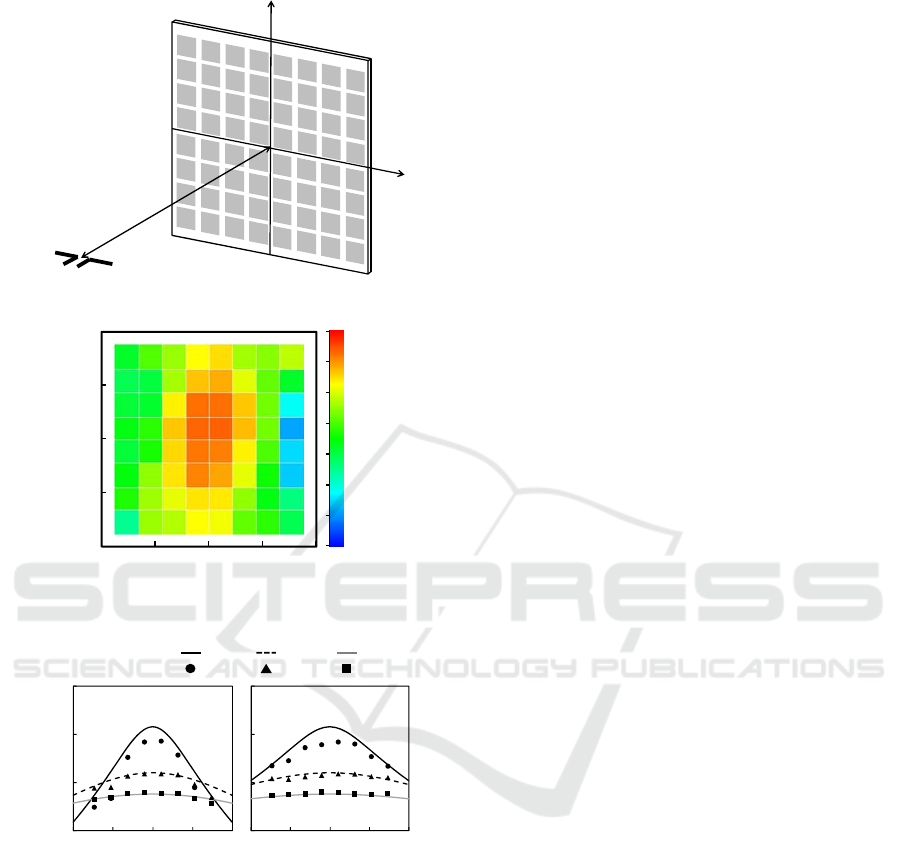
Figure 10: Measurement of RF power distribution: (a)
experimental setup, (b) power distribution at 10 cm from
the transmitter, and (c) horizontal and vertical profiles of
power distribution.
3.3 RF Amplitude and Phase
Distribution Measurement
On the basis of the developed technique, RF
amplitude and phase distributions can also be
obtained. By measuring the amplitude and phase of
the voltages induced on each individual resistor, we
are able to calculate those of the electric field
incident upon it. This has been quantitatively
confirmed by simulation (Yagitani et al., 2013).
However, it was revealed that edge reflection from a
finite-sized absorber created a specific interference
pattern on the amplitude and phase profiles on the
absorber surface, thereby degrading the accuracy of
the measurement. Though the interference pattern
depended on the absorber size and frequency,
generally the central area of the absorber had the
highest measurement accuracy (less than 10%
errors). Reduction in the edge reflection should be
desired for practical use of this technique.
One application of amplitude and phase
measurement is polarization identification. As
explained in Section 3.2, the metamaterial absorber
measures independently two orthogonal
polarizations in the x- and y-directions. From the
phase information in addition to the amplitude,
linear, circular and elliptical polarizations are
identified, including their major and minor axial
directions as well as their sense of polarization, i.e.,
right- or left-handed (see also Section 4.2).
Another application is the direction finding and
localization of RF sources. Ideally, when an
incident RF wave is completely absorbed, each
individual resistor (being as an amplitude and phase
sensor) does not act as a scatterer so that no mutual
coupling between the resistors is expected.
Therefore the matrix of resistors on the absorber
would work as an ideal antenna array. The present
technique could be applied to obtaining the
directions-of-arrival (DOAs) of the incoming RF
signals from far sources, invoking various DOA
estimation techniques such as MUSIC, ESPRIT, and
others. The estimated source directions could even
be visualized on a real image (Kwakkernaat et al.,
2008). Source localization will be realized also for
near-field sources. The near-field localization
techniques such as radio holography (Kitayoshi and
Sawaya, 1999), MUSIC (Kato et al., 2005) and SPM
(Yoshimoto et al., 2005) could be used to obtain
source locations and shapes, along with source
visualization (Taira et al., 2004).
4 IN-SITU VISUALIZATION OF
ELECTROMAGNETIC FIELDS
In general, an EM sensor measures an EM field and
converts it to electric signals, which are then
transferred to receivers, and processed and displayed
on a PC when necessary. The authors have been
working to develop the EM sensor having the
capability of visualizing the measured field
-20 0 20
-20
0
20
x [cm]
y [cm]
-25
-60
Absorbed power [dBm]
(b)
x
y
TX dipole
d
O
Metamaterial
absorber
(a)
‐50
‐40
‐30
‐20
-20 -10 0 10 20
‐50
‐40
‐30
‐20
-20 -10 0 10 20
-20 0 20 -20 0 20
-20
Horizontal axis x [cm] Vertical axis y [cm]
Absorbed power [dBm]
(c)
(Theoretical) 10 cm 30 cm 50 cm
(Measured) 10 cm 30 cm 50 cm
Distance from TX
-50
-30
-40
Second International Conference on Telecommunications and Remote Sensing
26
immediately adjacent to the sensor itself, thereby
one could intuitively figure out the in-situ field
properties such as the intensity, vector direction and
polarization. In this chapter new techniques under
development based on this concept are described.
4.1 Electromagnetic Vector Compass
One example of such a system is an
“Electromagnetic Vector Compass.” The 3d vector
direction of the in-situ EM field measured by an EM
vector sensor is displayed on the surface of the
sensor housing itself, as illustrated in Figure 11.
Figure 12 shows a prototype of the vector compass
for low-frequency AC magnetic field. A tri-axial
search coil sensor is used to measure magnetic field
vectors, which are processed by built-in receivers
and displayed on an OLED screen attached on each
of the six surfaces of the cubic housing. The screen
on each surface plots an arrow representing the
projection of the measured 3d vectors onto that
surface. Just like an ordinary magnetic compass (for
dc magnetic field), it displays in-situ EM vectors in
real-time. With this kind of compact sensor one is
able to observe the magnetic vectors in his/her hand,
just at the point of measurement.
Figure 11: Electromagnetic vector compass.
Figure 12: AC magnetic vector compass.
4.2 In-situ RF imaging Screen
In-situ visualization of RF fields is more difficult,
since the sensor itself, cables, receivers and displays
may reflect, scatter and disturb the field of interest.
As explained in Chapter 3, we have developed a
metamaterial absorber capable of measuring incident
RF power, amplitude and phase distributions. If the
absorber is made of transparent materials and a
display screen is placed just behind it, we would be
able to construct an “in-situ RF imaging screen” as
illustrated in Figure 13. The 2d distribution of RF
field absorbed on the surface is measured by
embedded power (or amplitude and phase) detectors,
which is transferred to the display and immediately
visualized there. Thus the image of RF field is
visualized in-situ, just as if a wall is illuminated by a
flashlight.
Figure 13: In-situ RF imaging screen.
Figure 14: In-situ visualization of RF polarization.
A transparent absorber was fabricated,
employing a transparent acrylic substrate and a
transparent sheet of fine metal mesh. Transparent
resistive films usually used to realize transparent
absorbers (e.g., Haruta et al., 2000) were not adopted
here because they have resistivity to absorb the RF
field by themselves, whereas in the present absorber
the RF power should be dissipated mainly in the
lumped resistors. The size of the absorber was 30
cm square with 2-mm thickness. On the backside of
the absorber amplitude and phase detectors were
attached to measure two orthogonal polarizations.
EM field
EM Compass
Amplitude and
phase detectors
(embedded)
Display
Transparent absorber
Visualizing amplitude,
polarization, etc.
TX dipole
In-Situ Measurement and Visualization of Electromagnetic Fields
27

Figure 14 shows a preliminary demonstration of in-
situ visualization of polarization. A 1.7-GHz wave
was transmitted from a dipole antenna and measured
by the transparent absorber. The measured
polarization at the center of the absorber was plotted
on a PC display placed just behind the absorber. In
this case the transmitted wave became an elliptically
polarized, possibly due to the reflection from the
table or cables.
5 CONCLUSIONS
Various in-situ measurement and visualization
techniques and systems for EM fields were reported
which have been developed by the authors’ group.
Using the developed systems, the EM fields can be
captured and visualized in situ and in real-time.
Such systems are expected to be quite useful for
measuring EM field distributions in various
scenarios in the fields of EMC, antennas and
propagation. The systems could be applicable to
quick noise measurement at the development stage
of electric or electronic equipment, as well as to the
in-situ measurement of EM field distributions in the
actual environments such as offices, factories, cars,
trains and airplanes. Last but not least, such
visualization techniques could contribute to
education in electromagnetics and radio engineering,
where students will be able to virtually observe the
actual EM fields in various situations.
ACKNOWLEDGEMENTS
The authors would like to thank (ex-) students of
Kanazawa University: Messrs. Y. Yamanaka, T.
Shimizu, S. Morita, K. Katsuda, E. Tanaka, R.
Tanaka, M. Nojima, S. Shiraki, T. Nakagawa, T.
Sunahara, D. Hiraki, K. Iwasaki, N. Fukuoka and H.
Maeda for their help with design, fabrication and
measurement of the EM and RF measurement and
imaging systems.
REFERENCES
Baudry, D., Arcambal, C., Louis, A., Mazari, B., Eudeline,
P., 2007. Applications of the near-field techniques in
EMC investigations, IEEE Trans. Electromagnetic
Compatibility, vol.49, no.3, pp.485-493.
Chen, H., Zhang, H., Ni, Z., Li, R., 2012. Research on
imaging detection of RF leakage on the surface of
spacecraft, Proc. 2012 Int. Symp. EMC (EMC
EUROPE), pp.1-4.
Dutta, S. K., Vlahacos, C. P., Steinhauer, D. E.,
Thanawalla, A. S., Feenstra, B. J., Wellstood, F. C.,
Anlage, S. M., Newman, H. S., 1999. Imaging
microwave electric fields using a near-field scanning
microwave microscope, Applied Physics Letters,
vol.74, no.1, pp.156-158.
Fan, H., 2009. Far field radiated emission prediction from
magnetic near field magnitude-only measurements of
PCBs by Genetic Algorithm, Proc. IEEE Int. Symp.
EMC, pp.321-324.
Gao, Q., Yin, Y., Yan, D.-B., Yuan, N.-C., 2005. A novel
radar-absorbing-material based on EBG structure,
Microwave and Optical Technology Letters, vol.47,
no.3, pp.228-230.
Haelvoet, K., Criel, S., Dobbelaere, F., Martens, L., De
Langhe, P., De Smedt, R., 1996. Near-field scanner for
the accurate characterization of electromagnetic fields
in the close vicinity of electronic devices and systems,
Proc. IEEE Instrumentation and Measurement
Technology Conf., pp.1119-1123.
Haruta, M., Wada, K., Hashimoto, O., 2000. Wideband
wave absorber at X frequency band using transparent
resistive film, Microwave and Optical Technology
Letters, vol.24, no.4, pp.223-226.
Kato, T., Taira, K., Sawaya, K., Sato, R., 2005.
Estimation of short range multiple coherent source
location by using MUSIC algorithm, IEICE Trans.
Commun., vol.E88-B, no.8, pp.3317-3320.
Kazama, S., Arai, K. I., 2002. Adjacent electric field and
magnetic field distribution measurement system, Proc.
IEEE Int. Symp. EMC, vol.1, pp.395–400.
Kitayoshi, H., Sawaya, K. 1999. Electromagnetic-wave
visualization for EMI using a new holographic method,
Electronics and Communications in Japan, Part 1,
vol.82, no.8, pp.52-60.
Kwakkernaat, M. R. J. A. E., de Jong, Y. L. C., BuItitude,
R. J. C., Herben, M. H. A. J., 2008. High-resolution
angle-of-arrival measurements on physically-
nonstationary mobile radio channels, IEEE Trans.
Antennas and Propagation, vol.AP-56, no.8, pp. 2720-
2729.
Laurin, J. J., Ouardhiri, Z., Colinas, J., 2001. Near-field
imaging of radiated emission sources on printed-
circuit boards, Proc. IEEE Int. Symp. EMC, vol.1,
pp.368-373.
Luukkonen, O., Costa, F., Simovski, C. R., Monorchio, A.,
Tretyakov, S. A., 2009. A thin electromagnetic
absorber for wide incidence angles and both
polarizations, IEEE Trans. Antennas and Propagation,
vol.57, no.10, pp.3119-3125.
Mias, C., Yap, J. H., 2007. A varactor-tunable high
impedance surface with a resistive-lumped-element
biasing grid,
IEEE Trans. Antennas and Propagation,
vol.55, no.7, pp.1955-1962.
Norgard, J., Musselman, R., 2004. CEM code validation
using infrared thermograms, Proc. 2004 Int. Symp.
EMC, pp.637-640.
Second International Conference on Telecommunications and Remote Sensing
28

Sasagawa, K., Kanno, A., Kawanishi, T., Tsuchiya, M.,
2007. Live electrooptic imaging system based on
ultraparallel photonic heterodyne for microwave near-
fields, IEEE Trans. Microwave Theory Tech., vol.55,
no.12, pp.2782-2791.
Sato, K., Miyata, N., Kamimura, Y., Yamada, Y., 2010. A
freehand scanning method for measuring EMF
distributions using magnetic tracker, IEICE Trans.
Commun., vol.E93-B, no.7, pp.1865-1868.
Sato, K., Kawata, H., Kamimura, Y., 2012. A freehand
scanning method for measuring EMF distributions,
IEICE Trans. Commun., vol.J95-B, No.2, pp.293-301.
(in Japanese)
Shi, J., Cracraft, M. A., Zhang, J., DuBroff, R. E., Slattery,
K., 2004. Using near-field scanning to predict radiated
fields, Proc. IEEE Int. Symp. EMC, pp.14-18.
Taira, K., Kato, T., Sawaya, K., Sato, R., 2004. Estimation
of source location of leakage field from transformer-
type microwave oven, Proc. 2004 Int. Symp. EMC,
vol.2, pp.489-493.
Tumanski, S., Liszka, A., 2002. The methods and devices
for scanning of magnetic fields, J. Magnetism and
Magnetic Materials, vol.242–245, pp.1253–1256.
Tumanski, S., Baranowski, S., 2006. Magnetic sensor
array for investigations of magnetic field distribution,
J. Electrical Engineering, vol.57, no.8/S, pp.185-188.
Yagitani, S., Okumura, E., Nagano, I., Yoshimura, Y.,
2007. Localization of low-frequency source current
distributions, Proc. 2007 Int. Symp. Antennas and
Propagation, pp.89-92.
Yagitani, S., Katsuda, K., Nojima, M., Yoshimura, Y.,
Sugiura, H., 2011a. Imaging radio-frequency power
distributions by an EBG absorber, IEICE Trans.
Commun., vol.E94-B, no.8, pp.2306-2315.
Yagitani, S., Katsuda, K., Tanaka, R., Nojima, M.,
Yoshimura, Y., Sugiura, H., 2011b. A tunable EBG
absorber for radio-frequency power imaging, Proc.
30th URSI GASS, 4 pages.
Yagitani, S., Sunahara, T., Nakagawa, T., Hiraki, D.,
Yoshimura, Y., Sugiura, H., 2013. Radio-frequency
field measurement using thin artificial magnetic
conductor absorber, Proc. 2013 Int. Symp.
Electromagnetic Theory, 4 pages.
Yamaguchi, M., Yabukami, S., Yurugi, H., Nakada, K.,
Arai, K. I., Itagaki, A., Itagaki, K., Saito, N., Fuda, K.,
Watanabe, M., Takahashi, H., Tamogami, T.,
Sakurada, Y., 1999. Two dimensional electromagnetic
noise imaging system using planar shielded-loop coil
array, Proc. 1999 Int. Symp. EMC, pp.51-54.
Yoshimoto, Y., Taira, K., Sawaya, K., Sato, R., 2005.
Estimation of multiple coherent source locations by
using SPM method combined with signal subspace
fitting technique, IEICE Trans. Commun., vol.E88-B,
no.8, pp.3164-3169.
In-Situ Measurement and Visualization of Electromagnetic Fields
29
